Article

Investigation of the Optimum Mg Doping Concentration in p-Type-Doped Layers of InGaN Blue Laser Diode Structures

Department of Physics, Inha University, 100 Inha-ro, Michuhol-gu, Incheon 22212, Korea
*
Author to whom correspondence should be addressed.
Crystals 2021, 11(11), 1335; https://doi.org/10.3390/cryst11111335
Submission received: 18 October 2021 / Revised: 28 October 2021 / Accepted: 30 October 2021 / Published: 1 November 2021
(This article belongs to the Special Issue Advances in GaN-Based Optoelectronic Materials and Devices)

Abstract

:
In GaN-based laser diode (LD) structures, Mg doping in p-type-doped layers has a significant influence on the device performance. As the doping concentration increases, the operation voltage decreases, whereas the output power decreases as a result of increased optical absorption, implying that optimization of the Mg doping concentration is required. In this study, we systematically investigated the effect of the Mg doping concentration in the AlGaN electron-blocking layer (EBL) and the AlGaN p-cladding layer on the output power, forward voltage, and wall-plug efficiency (WPE) of InGaN blue LD structures using numerical simulations. In the optimization of the EBL, an Al composition of 20% and an Mg doping concentration of 3 × 1019 cm−3 exhibited the best performance, with negligible electron leakage and a high WPE. The optimum Mg concentration of the p-AlGaN cladding layer was found to be ~1.5 × 1019 cm−3, where the maximum WPE of 38.6% was obtained for a blue LD with a threshold current density of 1 kA/cm2 and a slope efficiency of 2.1 W/A.

Graphical Abstract

1. Introduction

After the first development of nitride laser diodes (LDs) in 1996 [1] and first demonstration of blue LDs in 2001 [2] by Nichia, the performance of blue LDs has improved considerably. To date, InGaN/GaN-based blue LDs have attracted significant attention for use in light sources for laser displays [3,4,5], laser-based white lighting [6,7,8], free-space or underwater communications [9,10,11], and laser-based materials processing [12,13,14]. In recent years, high-power operation of InGaN blue LDs with >5 W output power in a single chip has been demonstrated, mainly by company research groups such as Nichia, Osram, and Sony [3,4,12]. They also reported the low-threshold and high-efficiency operation of blue LDs with a threshold current density (Jth) < 1 kA/cm2, slope efficiency (SE) > 2 W/A, and wall-plug efficiency (WPE) > 40% [3,12]. Very recently, a university research group at Xiamen university also reported comparable performance of a blue LD with a Jth of ~1 kA/cm2 and an SE of 1.8 W/A [15].
Despite the remarkable progress in the development of high-power and high-efficiency blue LDs, the performance of InGaN blue LDs is still inferior to that of GaAs-based infrared LDs, which demonstrated a WPE of even more than 70% [16]. Mg doping in p-type-doped layers of GaN-based LDs is one of the main factors limiting the WPE. Owing to the high acceptor activation energy of Mg in (Al)GaN and the low mobility of hole carriers, the resistivity of p-type-doped layers in GaN-based LD structures is considerably larger than that of n-type layers, which results in a high operation voltage. To improve the conductivity of the p-AlGaN cladding layer and prevent electron leakage over the AlGaN electron-blocking layer (EBL), high-concentration Mg doping is required to increase the hole concentration. The low conductivity of the p-type layers is one of the main reasons limiting the WPE of GaN-based LDs [17,18].
However, optical absorption in heavily-doped p-type layers is one of the main causes of internal loss in GaN-based LDs [18,19,20,21,22,23,24]. The absorption coefficient of Mg-doped p-type layers increases with increasing doping concentration as a result of free-carrier absorption [25,26]. The absorption coefficient of p-type layers in GaN-based LDs has been reported to be in several tens of cm−1, which could significantly decrease the SE and, hence, the laser output power of an LD. To reduce the modal loss associated with p-type doping, a thick undoped waveguide layer has been employed between multiple-quantum-well (MQW) active layers and a p-AlGaN cladding layer [19,21,22,23,24]. The optical loss can also be decreased by decreasing the Mg doping concentration in the p-type layers. However, the operation voltage could be increased as the thickness of the undoped layer increases or the Mg doping concentration of the p-type layers decreases. Hence, there is a trade-off relationship between the operation voltage and laser output power with variation in the doping concentration of Mg, which implies that there exists an optimum Mg doping concentration in the p-type-doped layers in GaN-based LD structures. Meanwhile, there is a wide variation in the reported Mg doping concentration, ranging from <1 × 10¹⁸ to 5 × 1019 cm−3 [23,24,27,28,29,30], and there has been a lack of studies on the optimum Mg doping concentration in the p-type layers of InGaN blue LD structures.
In this study, we investigated the optimum Mg doping concentrations in the p-type AlGaN EBL and cladding layers of InGaN blue LD structures using numerical simulations. For the simulation of the LD device characteristics, we employed a simulation software application, LASer Technology Integrated Program (LASTIP), produced by Crosslight Co. [31]. Regarding the optimization processes of this study, the thickness of the waveguide layers below and above the MQW was first optimized to obtain a high optical confinement factor (OCF) and low-threshold operation. Next, we investigated the effects of the Al composition and Mg doping concentration in the p-AlGaN EBL on the electron leakage current and LD characteristics. Finally, the Mg doping concentration in the p-AlGaN cladding layer was optimized to obtain the highest WPE for high-power operation.

2. Materials and Methods

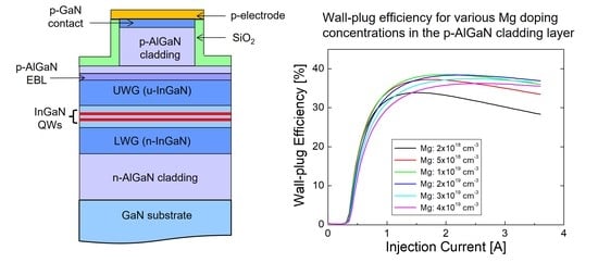
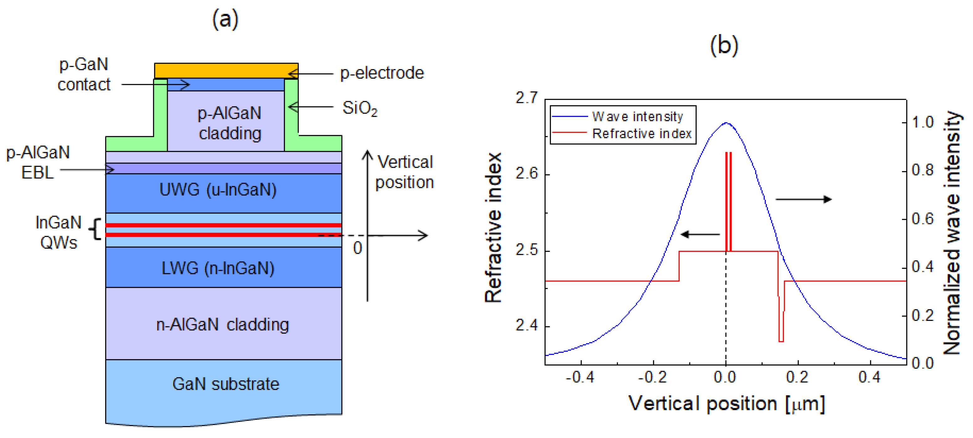
2.1. Laser Diode Structure

Figure 1a schematically shows the blue LD structure used in the simulation of this study. The LD epitaxial layer structures were composed of a 1-μm thick n-Al0.04Ga0.95N cladding layer, an n-In0.02Ga0.98N lower waveguide (LWG), MQW active region, an In0.02Ga0.98N upper waveguide (UWG), a 15-nm thick p-AlGaN EBL, a 0.6-μm thick p-Al0.04Ga0.95N cladding layer, and a 20-nm thick p-GaN contact layer grown on a GaN substrate. The active region consisted of two 3-nm In0.15Ga0.85N QW layers separated by a 10-nm In0.02Ga0.98N barrier layer. For this MQW structure, the emission wavelength of the LD was 450 nm at 25 °C. A recent study revealed that a blue LD structure with two InGaN QWs exhibits the best performance [15]. The QW and barrier layers in the active region were undoped. The doping concentrations of the n-type doped layers, such as the n-GaN substrate, the n-AlGaN cladding layer, and the In0.02Ga0.98N LWG, were all assumed to be 5 × 1018 cm−3. While the LWG was doped with an n-type dopant, the UWG was left undoped to avoid significant optical absorption loss, which might otherwise be caused by p-type doping [19,21,22,23,24]. However, the undoped MQW and UWG regions were assumed to have an unintentionally doped background electron concentration of 5 × 1016 cm−3 [23,29]. The doping concentration of the p-GaN contact layer was set to 2 × 1019 cm−3.
In the simulated LD structure, the UWG was positioned between the MQW and EBL. This layer arrangement has been known to be advantageous for reducing the absorption loss caused by the Mg-doped EBL [21,22,23,24] and preventing the diffusion of Mg dopant into the active region [32,33,34]. The LD chip structure had the form of a broad area ridge waveguide with a ridge width of 30 μm and a cavity length of 1200 μm for high-power operation. The reflectivities of the front and rear facet were assumed to be 5% and 95%, respectively. In the simulation, we investigated the LD characteristics by varying the thickness of the LWG and UWG, the composition and doping concentration of the EBL, and the doping concentration of the p-AlGaN cladding layer.

2.2. Simulation Methods

The device characteristics, such as the output power versus current relation (L–I curve) and the forward voltage versus current relation (V–I curve), were simulated using LASTIP. It self-consistently solves QW band structures, radiative and nonradiative carrier recombination, the drift and diffusion equation of carriers, and the photon rate equations [31]. The built-in polarization fields induced by spontaneous and piezo-electric polarizations at the hetero-interfaces, such as InGaN/GaN, AlGaN/GaN, and InGaN/AlGaN, were also included using the model described in Ref. [35], assuming a 50% compensation for the polarization fields [36,37]. Then, the strength of the polarization fields at the interfaces between the In0.15Ga0.85N QW and GaN barrier was approximately 1 MeV/cm, which roughly corresponds to the reported internal electric fields of In0.15Ga0.85N/GaN MQWs [38,39]. The conduction band offset of the hetero-barriers was set to be 0.7 [17]. For this band offset value, the corresponding barrier heights of the conduction band between In0.15Ga0.85N/In0.02Ga0.98N QWs and In0.02Ga0.89N/Al0.2Ga0.8N EBL were 430 and 295 meV, respectively. The mobility model described in Refs. [40,41,42] was used for the mobility of electrons, which resulted in an electron mobility of ~500 cm2/Vs for n-GaN with a doping concentration of 1 × 1018 cm−3. The hole mobilities in the InGaN and (Al)GaN layers were assumed to be 5 and 15 cm2/Vs, respectively [31,41].
Using the refractive index data of GaN, AlGaN, and InGaN alloys at 450 nm from Refs. [25,43,44,45], the refractive indices of the GaN layer, Al0.04GaN cladding layers, and In0.02GaN waveguides were chosen to be 2.48, 2.46, and 2.50, respectively. Figure 1b shows the profiles of the refractive index and wave intensity of the lasing mode as a function of the vertical position when the thicknesses of both the LWG and UWG are 120 nm, and the Al composition of the EBL is 20%. The origin of the vertical position corresponds to the bottom interface of the n-side QW. As shown in Figure 1b, the lasing mode is symmetrically distributed and centered at the QW layers to obtain a high OCF value. In this case, the OCF was calculated to be ~1.5%. This OCF value is similar to that of previously reported InGaN blue LD structures with double QW layers, with a similar QW thickness [22,24,28]. To model the optical absorption loss, we adopted a first-principle calculation model for free-carrier absorption derived from Ref. [26], which showed an absorption cross-section of ~0.6 × 10⁻¹⁸ cm2 for both the donor and acceptor dopants. According to Ref. [26], both free holes and acceptor-bound holes contribute to the optical absorption process in the p-type-doped layers. Therefore, the absorption coefficient could be obtained by multiplying the absorption cross-section by the Mg doping concentration. For example, the absorption coefficient of n-type layers with a doping concentration of 5 × 1018 cm−3 and that of a p-type layer with a doping concentration of 2 × 1019 cm−3 were set as 3 and 12 cm−1, respectively. In addition to the free-carrier absorption, the background absorption coefficient, which might account for the scattering losses or absorption in metals, was assumed to be 2 cm−1.
Owing to the high acceptor activation energy of Mg, the actual hole concentration in the p-type-doped region would be significantly lower than the Mg doping concentration. In the simulation, the incomplete ionization of Mg acceptor atoms in the p-type-doped layers was included, and the acceptor ionization energy in AlGaN was assumed to scale linearly from 170 meV (GaN) to 470 meV (AlN) [17,46]. For an acceptor doping concentration of Na, the ratio of hole concentration p to Na is given by [47]
p N a = 1 1 1 + g a 1 exp [ ( E F E a ) / k T ]
where EF, Ea, k, and T are the Fermi energy level, acceptor ionization energy, Boltzmann constant, and the absolute temperature, respectively. ga is called a degeneracy factor, which is normally taken as 4 for acceptors. The Lastip program calculated the actual hole concentration in Mg-doped region using Equation (1). Figure 2 shows the hole concentration and ratio of ionized Mg acceptors at the p-Al0.05GaN cladding layer as a function of the Mg doping concentration. As the Mg doping concentration increased from 2 × 10¹⁸ to 5 × 1019 cm−3, the hole concentration increased slowly from 0.07 × 10¹⁸ to 0.37 × 1018 cm−3 and the ratio of ionized Mg acceptors decreased from 3.7% to 0.75%. As a result of the low ionization ratio of Mg, the actual hole concentration was far below 1018 cm−3 in AlGaN, even for a high Mg doping concentration > 1019 cm−3.
In the carrier recombination model of LASTIP, the radiative recombination rate is calculated by integrating the spontaneous emission spectrum with a Lorentzian line-shape function. The Shockley–Read–Hall (SRH) recombination lifetime was assumed to be 50 ns. However, the effect of SRH recombination on the threshold current was found to be almost negligible when the SRH lifetime was longer than 10 ns. The lasing threshold of the InGaN blue LDs is strongly influenced by the Auger recombination coefficient (C) [18,45]. In the current simulations, C was chosen to be 2 × 1030 cm−6/s for the simulated blue LD to exhibit a Jth of ~1 kA/cm2. Figure 3a shows the L–I curve of the simulated LD structure using the parameters described above. Here, the thicknesses of the LWG and UWG were 120 nm, the Al composition and doping concentration of the EBL were 20% and 3 × 1019 cm−3, respectively, and the doping concentration of the p-AlGaN cladding layer was 1.5 × 1019 cm−3. In the subsequent section, we show that these values are close to the optimum values to achieve the highest WPE. The L–I curve in Figure 3a shows a threshold current of 350 mA and an SE of 2.1 W/A. The Jth value was estimated to be 0.98 kA/cm2 by dividing the threshold current by the cavity length and the ridge width. These Jth and SE values approximately correspond to those recently reported for high-power blue LDs [4,14,15]. Figure 3b shows the WPE as a function of injection current. A peak WPE of ~38% was obtained at 2 A, and a high WPE > 35% was maintained up to 3.6 A. In the simulation, the temperature of the LD structures was set at 298 K and self-heating effects were not considered. Therefore, the simulation results correspond to the pulsed operation condition with negligible thermal effects.

3. Results and Discussion

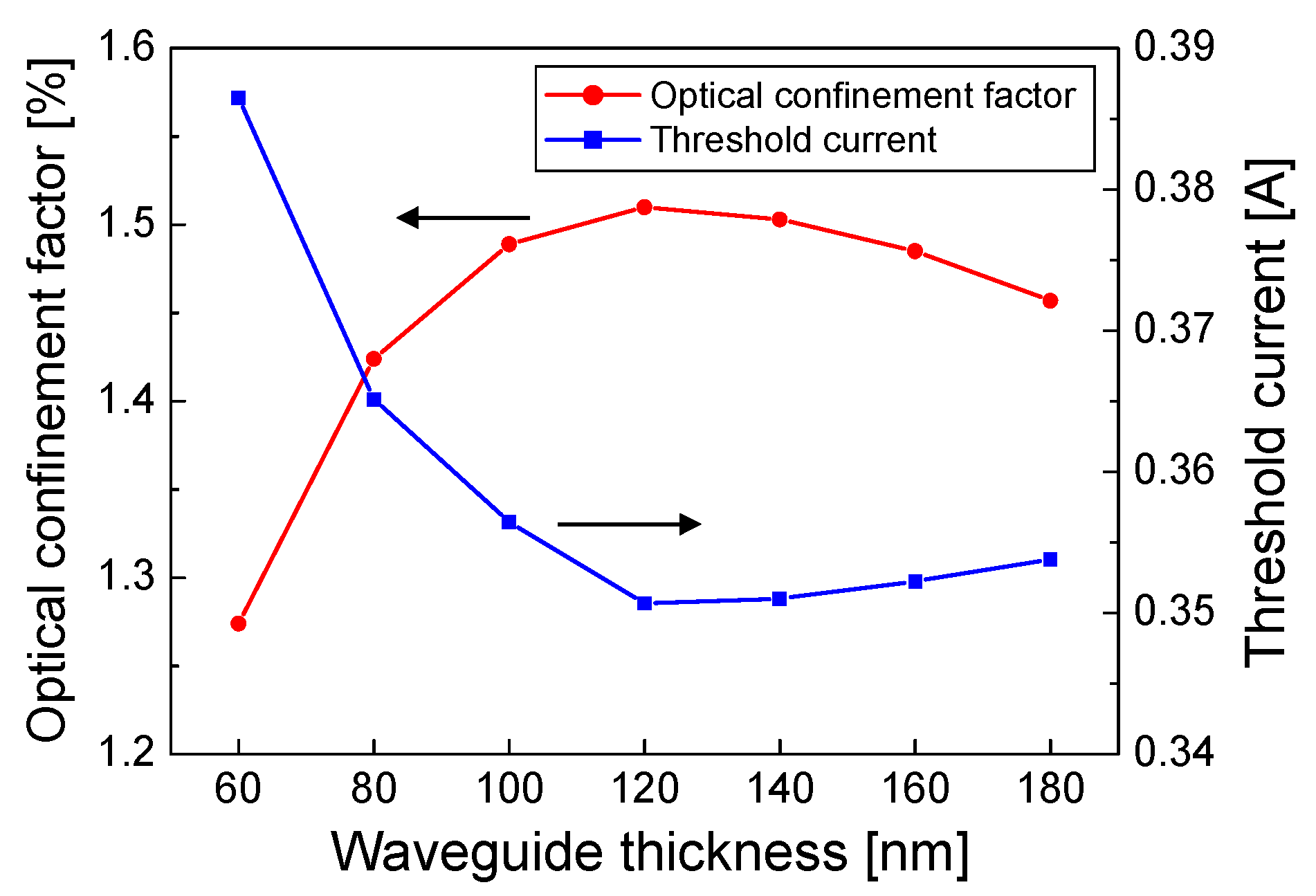
3.1. Optimum Thickness of LWG and UWG

The effects of the LWG and UWG on the OCF and lasing threshold were investigated to find the optimum waveguide thickness. Figure 4 shows the OCF and lasing threshold as a function of the waveguide thickness. In the simulation, the thicknesses of the LWG and UWG were simultaneously varied. Initially, the OCF increased with the waveguide thickness from 60 to 120 nm as a result of increased optical confinement in the In0.02Ga0.98N LWG and UWG layers. When the thickness was larger than 120 nm, the OCF began to decrease because the portion of the lasing mode profile within the QW layers decreased with the waveguide thickness for sufficiently thick waveguides. Therefore, the highest OCF was obtained for the LWG and UWG thickness of 120 nm. As shown in Figure 4, the threshold current was inversely proportional to the OCF, and the lowest threshold current could also be obtained for the LWG and UWG thickness of 120 nm. Therefore, the optimum thickness of the LWG and UWG layers was chosen to be 120 nm for subsequent simulations in this study.

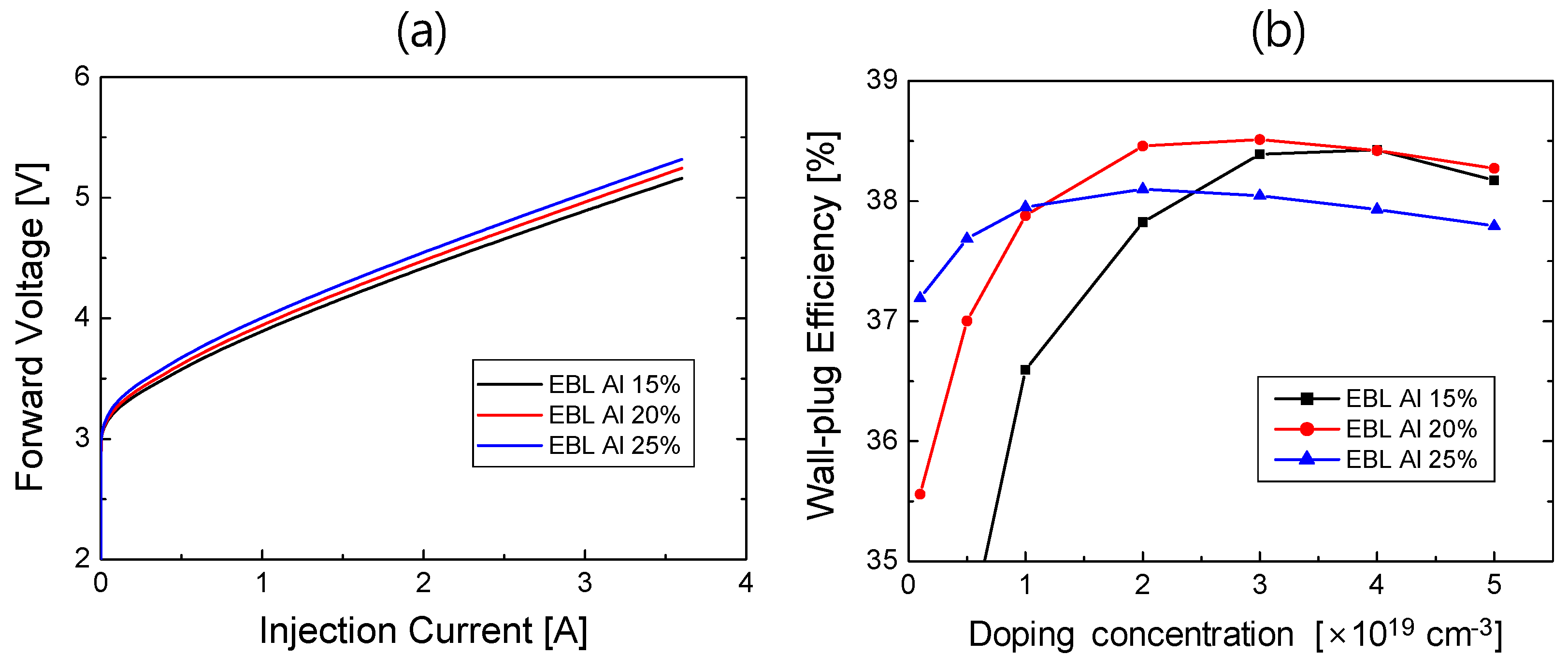
3.2. Optimization of EBL

Next, we investigated the effects of the Al composition and Mg doping concentration in the EBL on the LD performance. The role of the EBL is to prevent electron leakage from the MQW to the p-cladding layers. Therefore, the electron leakage current was first calculated for variation in the Al composition and doping concentration of the EBL. Figure 5 shows the portion of electron leakage current as a function of Mg doping concentration in the EBL for the Al compositions of 15%, 20%, and 25%. The portion of the leakage current, which is denoted as f, is defined as
f = J n y ( p - AlGaN ) J n y ( n - AlGaN )
where J n y (n-AlGaN) and J n y (p-AlGaN) are the vertical component of electron current density at the n-AlGaN and p-AlGaN cladding layer, respectively. As shown in Figure 5, f decreased as both the doping concentration and the Al composition increased. To obtain an f value < 1%, the required Mg doping concentration was ~5 × 10¹⁹, ~3 × 10¹⁹, and ~1.5 × 1019 cm−3 for the Al compositions of 15%, 20%, and 25%, respectively. It can be observed from Figure 5 that a high Mg doping concentration and Al composition were advantageous for preventing electron leakage. In this simulation, the Mg doping concentration in the p-AlGaN cladding layer was fixed at 1.0 × 1019 cm−3. However, it was found by separate simulations that the data in Figure 5 are almost independent of the Mg doping concentration.
Figure 6 shows the L–I curves of the LDs for various Mg-doping concentrations from 1.0 × 10¹⁸ to 5 × 1019 cm−3. When the Al composition of the EBL was 15% (Figure 6a), the output power at a high injection current decreased as the Mg doping concentration decreased because of increasing of the electron leakage with decreasing of the doping concentration, as shown in Figure 5. The output power did not decrease when the doping concentration was higher than 3 × 1019 cm−3, which resulted from the negligible electron leakage for this high doping concentration. When the Al composition of the EBL was 20% (Figure 6b), the output power also decreased with the decreasing of the Mg doping concentration. However, the decrease in power was significantly reduced compared with that observed in the case of 15%-Al composition. When the doping concentration was equal to or higher than 2 × 1019 cm−3, the L–I curves were almost the same for different doping concentrations. When the Al composition of the EBL was increased to 25% (Figure 6c), the L–I curves were almost the same for all doping concentrations from 1.0 × 10¹⁸ to 5 × 1019 cm−3. However, a slight decrease in output power with the increasing of the Mg doping concentration was observed at a high current, which resulted from the increased optical absorption with the increasing of the doping concentration. Because the thickness of the EBL was only 15 nm, the Mg doping in the EBL had a negligible influence on the optical absorption.
The results in Figure 5 and Figure 6 show that high Al composition and high Mg doping concentration in the EBL were advantageous for obtaining high output power by suppressing electron leakage. However, the high Al composition in the EBL could increase the forward voltage because the EBL also acted as an energy barrier for holes. In Figure 7a, the V–I curves are compared for the Al compositions of 15%, 20%, and 25%. As expected, the forward voltage increased with the increasing of the Al composition of the EBL. This implies a trade-off relationship between the electron leakage current and forward voltage with variation in the Al composition of the EBL. Figure 7b shows the WPE as a function of the Mg doping concentration for the Al compositions of 15%, 20%, and 25%. There existed a maximum WPE value for each Al composition as the doping concentration varied. The Mg doping concentration for which the maximum WPE was observed decreased from 4 × 10¹⁹ to 2 × 1019 cm−3 as the Al content increased from 15% to 25%. As shown in Figure 7b, the maximum WPE of 38.5% could be obtained when the Al composition was 20% and the Mg doping concentration was 3 × 1019 cm−3. Therefore, we chose these values as the optimum EBL parameters for the following simulations.

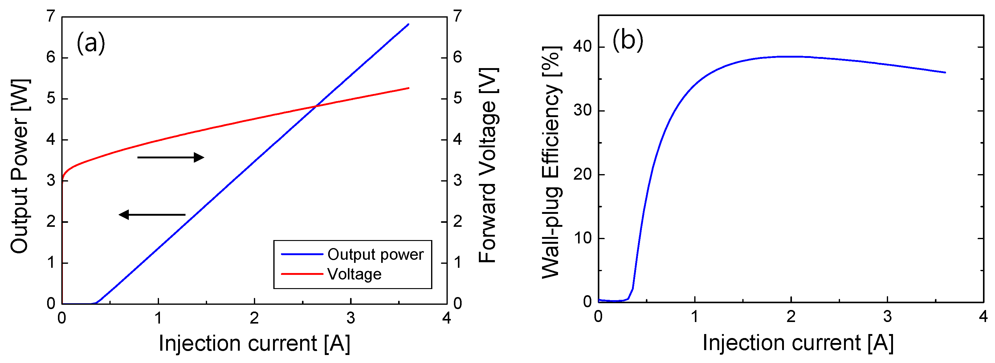
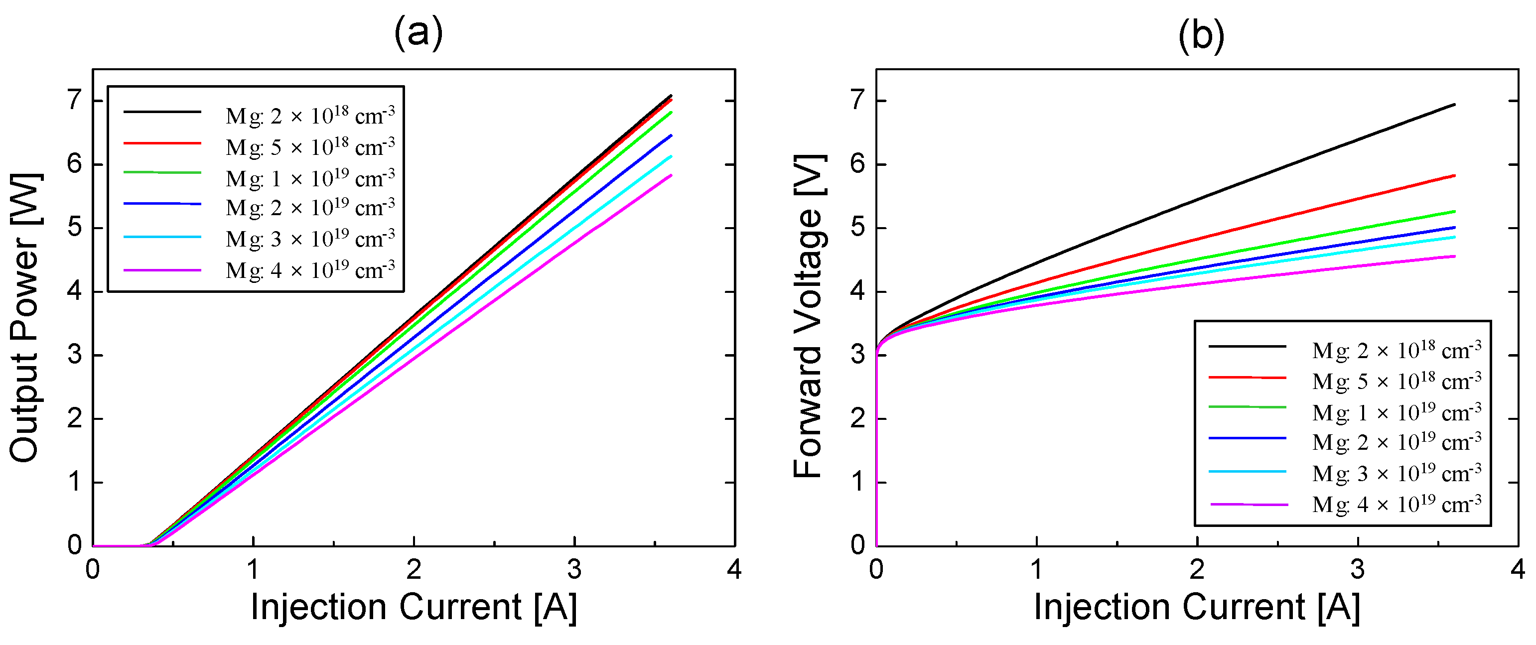
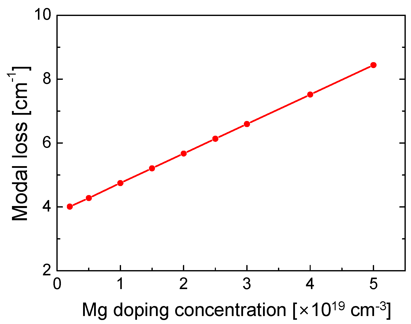
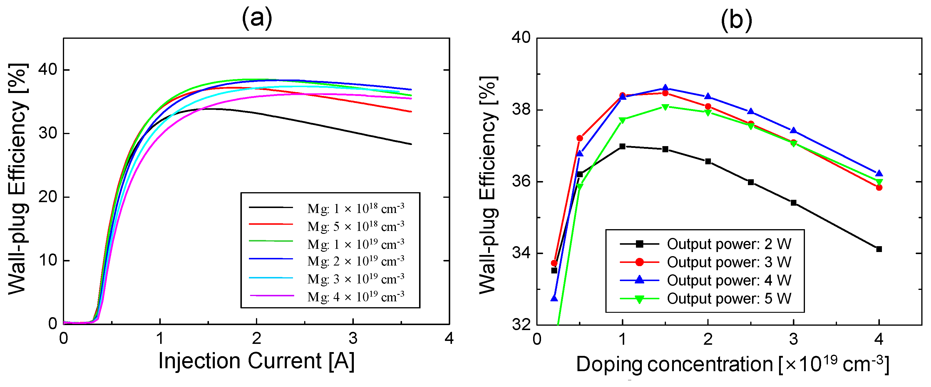
3.3. Optimum Mg Doping Concentration in the p-AlGaN Cladding Layer

In this subsection, we investigate the effect of the Mg doping concentration in the p-AlGaN cladding layer on the LD device performance. To see the effect of the Mg doping on total internal optical loss, the modal loss was calculated as the Mg doping concentration varied. Figure 8 shows the modal loss as a function of the Mg doping concentration from 2 × 10¹⁸ to 5 × 1019 cm−3 in the p-cladding layer. The modal loss increased linearly from 4 to 8.4 cm−1 as the Mg doping concentration increased from 2 × 10¹⁸ to 5 × 1019 cm−3, indicating significant influence of the Mg doping on optical loss. The modal loss shown in Figure 8 is similar to that of a previously reported LD structure with an SE of ~2 W/A [23].
Figure 9 shows the L–I and V–I curves for various Mg doping concentrations from 2 × 10¹⁸ to 4 × 1019 cm−3 in the p-cladding layer. According to the simulation results in Figure 4 and Figure 7, the thicknesses of the LWG and UWG were set as 120 nm, and the Al composition and Mg doping concentration of the p-AlGaN EBL were set as 20% and 3 × 1019 cm−3, respectively. In Figure 9a, it can be seen that the output power decreased significantly as the Mg doping concentration increased because of the increased optical absorption loss in the p-AlGaN cladding layer with the increasing of the doping concentration. The output power relatively decreased by ~24% as the doping concentration increased from 2 × 10¹⁸ to 4 × 1019 cm−3. In contrast, the forward voltage shown in Figure 9b decreased with the increasing of the Mg doping concentration, resulting from the improved electrical conductivity in the p-AlGaN cladding layer with the increasing of the Mg doping concentration. At an injection current of 3 A, the forward voltage decreased from 6.39 to 4.34 V as the doping concentrations increased from 2 × 10¹⁸ to 4 × 1019 cm−3.
As a result of the trade-off relationship between the output power and forward voltage with the variation of the Mg doping concentration, there existed an optimum Mg doping concentration where the maximum WPE could be obtained. Figure 10a shows the WPE as a function of the injection current for various Mg doping concentrations. When the doping concentration was 1 × 10¹⁹ and 2 × 1019 cm−3, the highest WPE was observed in a wide range of injection currents between 1 and 3.5 A. In Figure 10b, the WPE values are plotted as a function of the Mg doping concentration in the p-AlGaN cladding layer for the operation powers of 2, 3, 4, and 5 W. When the operation power of an LD was 2 W, the highest WPE of ~37% could be obtained at a doping concentration of 1 × 1019 cm−3. For the other operation powers of 3, 4, and 5 W, the maximum WPE of 38.1 ‒ 38.6% could be obtained at a doping concentration of 1.5 × 1019 cm−3. The highest WPE was obtained as 38.6% when the output power was 4 W and the doping concentration was 1.5 × 1019 cm−3. When the doping concentration was larger than 1.5 × 1019 cm−3, the WPE decreased gradually with the increasing of the doping concentration, owing to the increased optical absorption in the p-AlGaN layer. The decrease in the WPE for doping concentrations < 1 × 1019 cm−3 was attributed to the increase in the forward voltage due to the low hole concentration. Therefore, the optimum Mg doping concentration in the p-AlGaN cladding layer for the highest WPE was found to be 1.5 × 1019 cm−3, where the electrical conductivity and optical absorption were well balanced.
As mentioned previously, the presented simulation results corresponded to the pulsed operation condition without self-heating effects. Nevertheless, it would be meaningful to discuss the self-heating effect on the optimum doping concentration. In general, both the output power and forward voltage decrease as the temperature increases [48,49,50]. As shown in Figure 9, the output power and voltage also decreased with the increasing of the Mg doping concentration. That is, the temperature influenced the output power and forward voltage in the same manner as the doping concentration in the p-AlGaN cladding layer. Consequently, if the self-heating effect was included, the optimum Mg doping concentration would be expected to shift toward a higher level as a result of the temperature rise.

4. Conclusions

In this study, we performed a systematic study to determine the optimum Mg doping concentrations in the p-AlGaN EBL and p-AlGaN cladding layers of InGaN blue LD structures using numerical simulations. First, the thickness of waveguides layers below and above the MQW layers was optimized to achieve a high OCF and low lasing threshold. Next, the effect of the AlGaN EBL on the device performance was investigated. The optimum Al composition and doping concentration were determined to be 20% and ~3 × 1019 cm−3, respectively, which showed a negligible electron leakage current and a high WPE. Finally, the effect of the Mg doping concentration in the p-AlGaN cladding layer was investigated. The highest WPE was obtained for the Mg doping concentration of 1.5 × 1019 cm−3, where the forward voltage and output power were well balanced. For a blue LD with a threshold current density of 1 kA/cm2 and a slope efficiency of 2.1 W/A, a maximum WPE of 38.6% was obtainable under these optimum conditions. The simulation results revealed that the Mg doping concentration in p-type-doped layers has a significant influence on the WPE of InGaN blue LDs. The strategy to optimize the layer structures and doping concentrations of LDs presented in this study is expected to be advantageously applied in the development of high-power InGaN blue LD structures.

Author Contributions

Conceptualization, H.-Y.R.; methodology, C.O. and H.-Y.R.; software, C.O. and H.-Y.R.; validation, H.-Y.R.; investigation, C.O.; data curation, C.O.; writing—original draft preparation, C.O.; writing—review and editing, H.-Y.R.; supervision, H.-Y.R.; project administration, H.-Y.R.; funding acquisition, H.-Y.R. All authors have read and agreed to the published version of the manuscript.

Funding

This research was supported by the Basic Science Research Program through the National Research Foundation (NRF) of Korea, funded by the Ministry of Science and ICT (2019R1A2C1010160) and by the Technology Innovation Program (20015909) through the Korea Evaluation Institute of Industrial Technology (KEIT), funded by the Ministry of Trade, Industry & Energy (MOTIE, Korea).

Institutional Review Board Statement

Not applicable.

Informed Consent Statement

Not applicable.

Data Availability Statement

The data supporting the findings of this paper are available from the corresponding authors upon reasonable request.

Conflicts of Interest

The authors declare no conflict of interest. The funders had no role in the design of the study; in the collection, analyses, or interpretation of data; in the writing of the manuscript, or in the decision to publish the results.

References

  1. Nakamura, S.; Senoh, M.; Nagahama, S.; Iwasa, N.; Yamada, T.; Matsushita, T.; Kiyoku, H.; Sugimoto, Y. InGaN-based multi-quantum-well-structure laser diodes. Jpn. J. Appl. Phys. 1996, 35, L74–L76. [Google Scholar] [CrossRef]
  2. Nagahama, S.; Yanamoto, T.; Sano, M.; Mukai, T. Wavelength dependence of InGaN laser diode characteristics. Jpn. J. Appl. Phys. 2001, 40, 3075–3081. [Google Scholar] [CrossRef]
  3. Nakatsu, Y.; Nagao, Y.; Hirao, T.; Hara, Y.; Masui, S.; Yanamoto, T.; Nagahama, S. Blue and green InGaN semiconductor lasers as light sources for displays. Proc. SPIE 2020, 11280, 112800S. [Google Scholar]
  4. Murayama, M.; Nakayama, Y.; Yamazaki, K.; Hoshina, Y.; Watanabe, H.; Fuutagawa, N.; Kawanishi, H.; Uemura, T.; Narui, H. Watt-class green (530 nm) and blue (465 nm) laser diodes. Phys. Status Solidi A 2018, 215, 1700513. [Google Scholar] [CrossRef]
  5. Buckley, E. Laser wavelength choices for pico-projector applications. J. Disp. Technol. 2011, 7, 402. [Google Scholar] [CrossRef]
  6. Wierer, J.J.; Tsao, J.Y.; Sizov, D.S. Comparison between blue lasers and light-emitting diodes for future solid-state lighting. Laser Photonics Rev. 2013, 7, 963–993. [Google Scholar] [CrossRef]
  7. Ryu, H.Y.; Kim, D.H. High-brightness phosphor-conversion white light source using InGaN blue laser diode. J. Opt. Soc. Korea 2010, 14, 415–419. [Google Scholar] [CrossRef] [Green Version]
  8. Chi, Y.C.; Hsieh, D.H.; Lin, C.Y.; Chen, H.Y.; Huang, C.Y.; He, J.H.; Ooi, B.; DenBaars, S.P.; Nakamura, S.; Kuo, H.C.; et al. Phosphorous diffuser diverged blue laser diode for indoor lighting and communication. Sci. Rep. 2015, 5, 18690. [Google Scholar] [CrossRef] [PubMed] [Green Version]
  9. Watson, S.; Tan, M.; Najda, S.P.; Perlin, P.; Leszczynski, M.; Targowaski, G.; Grzanka, S.; Kelly, A.E. Visible light communications using a directly modulated 422 nm GaN laser diode. Opt. Lett. 2013, 38, 3792–3794. [Google Scholar] [CrossRef]
  10. Lee, C.; Zhang, C.; Cantore, M.; Farrell, R.M.; Oh, S.H.; Margalith, T.; Speck, J.S.; Nakamura, S.; Bowers, J.E.; DenBaars, S.P. 4 Gbps direct modulation of 450 nm GaN laser for high-speed visible light communication. Opt. Express 2015, 23, 16232–16237. [Google Scholar] [CrossRef]
  11. Wu, T.C.; Chi, Y.C.; Wang, H.Y.; Tsai, C.T.; Lin, G.R. Blue laser diode enables underwater communication at 12.4 Gbps. Sci. Rep. 2017, 7, 40480. [Google Scholar] [CrossRef] [PubMed]
  12. Baumann, M.; Balck, A.; Malchus, J.; Chacko, R.V.; Marfels, S.; Witte, U.; Dinakaran, D.; Ocylok, S.; Weinbach, M.; Bachert, C.; et al. 1000 W blue fiber-coupled diode laser emitting at 450 nm. Proc. SPIE 2019, 10900, 1090005. [Google Scholar]
  13. Coffey, V.C. High-powered diode lasers—New, bright and blue. Opt. Photonics News. 2020, 28–35. [Google Scholar] [CrossRef]
  14. Hagino, H.; Kawaguchi, M.; Nozaki, S.; Mochida, A.; Kano, T.; Takigawa, S.; Katayama, T.; Tanaka, T. High-power InGaN laser array with advanced lateral-corrugated waveguides. IEEE J. Quantum Electron. 2021, 57, 2600107. [Google Scholar] [CrossRef]
  15. Zhong, Z.; Lu, S.; Li, J.; Lin, W.; Huang, K.; Li, S.; Cai, D.; Kang, J. Design and fabrication of high power InGaN blue laser diode over 8 W. Opt. Laser Technol. 2021, 139, 106985. [Google Scholar] [CrossRef]
  16. Crump, P.; Wang, J.; Das, S.; Grimshaw, M.; Farmer, J.; DeVito, M.; Dong, W.; Crum, T.; Wise, D.; Feng, Y. >360 W and >70% efficient GaAs-based diode lasers. Proc. SPIE 2005, 5711, 21–29. [Google Scholar]
  17. Piprek, J. Comparative efficiency analysis of GaN-based light-emitting diodes and laser diodes. Appl. Phys. Lett. 2016, 109, 021104. [Google Scholar] [CrossRef]
  18. Piprek, J. Analysis of efficiency limitations in high-power InGaN/GaN laser diodes. Opt. Quantum Electron. 2016, 48, 471. [Google Scholar] [CrossRef]
  19. Uchida, S.; Takeya, M.; Ikeda, S.; Mizuno, T.; Fujimoto, T.; Matsumoto, O.; Goto, S.; Tojyo, T.; Ikeda, M. Recent progress in high-power blue-violet lasers. IEEE J. Sel. Top. Quantum Electron. 2003, 9, 1252–1259. [Google Scholar] [CrossRef]
  20. Ryu, H.Y.; Ha, K.H.; Son, J.K.; Paek, H.S.; Sung, Y.J.; Kim, K.S.; Kim, H.K.; Park, Y.; Lee, S.N.; Nam, O.H. Comparison of output power of InGaN laser diodes for different Al compositions in the AlGaN n-cladding layer. J. Appl. Phys. 2009, 105, 103102. [Google Scholar] [CrossRef]
  21. Chen, P.; Feng, M.X.; Jiang, D.S.; Zhao, D.G.; Liu, Z.S.; Li, L.; Wu, L.L.; Le, L.C.; Zhu, J.J.; Wang, H.; et al. Improvement of characteristics of InGaN-based laser diodes with undoped InGaN upper waveguide layer. J. Appl. Phys. 2012, 112, 113105. [Google Scholar] [CrossRef]
  22. Liang, F.; Zhao, D.; Jiang, D.; Liu, Z.; Zhu, J.; Chen, P.; Yang, J.; Liu, W.; Li, X.; Liu, S.; et al. New design of upper waveguide with unintentionally doped InGaN layer for InGaN-based laser diode. Opt. Laser Technol. 2017, 97, 284–289. [Google Scholar] [CrossRef]
  23. Kawaguchi, M.; Imafuji, O.; Nozaki, S.; Hagino, H.; Takigawa, S.; Katayama, T.; Tanaka, T. Optical-loss suppressed InGaN laser diodes using undoped thick waveguide structure. Proc. SPIE 2016, 9748, 974818. [Google Scholar]
  24. Hou, Y.; Zhao, D.; Liang, F.; Liu, Z.; Yang, J.; Chen, P. Enhancing the efficiency of GaN-based laser diodes by the designing of a p-AlGaN cladding layer and an upper waveguide layer. Opt. Mater. Express 2021, 11, 1780–1790. [Google Scholar] [CrossRef]
  25. Schubert, E.F. Light-Emitting Diodes, 2nd ed.; Cambridge University Press: Cambridge, UK, 2006; pp. 145–149. [Google Scholar]
  26. Kioupakis, E.; Rinke, P.; Van de Walle, C.G. Determination of internal loss in nitride lasers from first principles. Appl. Phys. Express 2010, 3, 082101. [Google Scholar] [CrossRef]
  27. Pourhashemi, A.; Farrell, R.M.; Cohen, D.A.; Speck, J.S.; DenBaars, S.P.; Nakamura, S. High-power blue laser diodes with indium tin oxide cladding on semipolar (202-1-) GaN substrates. Appl. Phys. Lett. 2015, 106, 111105. [Google Scholar] [CrossRef]
  28. Li, X.; Zhao, D.G.; Jiang, D.S.; Chen, P.; Liu, Z.S.; Zhu, J.J.; Yang, J.; Liu, W.; He, X.G.; Li, X.J.; et al. The effectiveness of electron blocking layer in InGaN-based laser diodes with different indium content. Phys. Status Solidi A 2016, 213, 2223–2228. [Google Scholar] [CrossRef]
  29. Wang, W.; Xie, W.; Deng, Z.; Liao, M. Improving output power of InGaN laser diode using asymmetric In0.15Ga0.85N/In0.02Ga0.98N multiple quantum wells. Micromachines 2019, 10, 895. [Google Scholar] [CrossRef] [PubMed] [Green Version]
  30. Cheng, L.; Li, Z.; Zhang, J.; Lin, X.; Yang, D.; Chen, H.; Wu, S.; Yao, S. Advantages of InGaN-GaN-InGaN delta barriers for InGaN-based laser diodes. Nanomaterials 2021, 11, 2070. [Google Scholar] [CrossRef] [PubMed]
  31. LASTIP by Crosslight Software Inc Burnaby Canada. Available online: http://crosslight.com (accessed on 1 October 2021).
  32. Chang, Y.L.; Ludowise, M.; Lefforge, D.; Perez, B. Study of Mg diffusion during metalorganic chemical vapor deposition of GaN and AlGaN. Appl. Phys. Lett. 1999, 74, 688–690. [Google Scholar] [CrossRef]
  33. Köhler, K.; Gutt, R.; Wiegert, J.; Kirste, L. Diffusion of Mg dopant in metal-organic vapor-phase epitaxy grown GaN and AlxGa1-xN. J. Appl. Phys. 2013, 113, 073514. [Google Scholar] [CrossRef]
  34. Nam, O.H.; Ha, K.H.; Kwak, J.S.; Lee, S.N.; Choi, K.K.; Chang, T.H.; Chae, S.H.; Lee, W.S.; Sung, Y.J.; Paek, H.S.; et al. Characteristics of GaN-based laser diodes for post-DVD applications. Phys. Status Solidi A 2004, 201, 2717–2720. [Google Scholar] [CrossRef]
  35. Fiorentini, V.; Bernardini, F.; Ambacher, O. Evidence for nonlinear macroscopic polarization in III-V nitride alloy heterostructures. Appl. Phys. Lett. 2002, 80, 1204–1206. [Google Scholar] [CrossRef]
  36. Flory, C.A.; Hasnain, G. Modeling of GaN optoelectronic devices and strain-induced piezoelectric effects. IEEE J. Quantum Electron. 2001, 37, 244–253. [Google Scholar] [CrossRef]
  37. Piprek, J. AlGaN polarization doping effects on the efficiency of blue LEDs. Proc. SPIE 2012, 8262, 82620E. [Google Scholar]
  38. Park, S.I.; Lee, J.I.; Jang, D.H.; Kim, H.S.; Shin, D.S.; Ryu, H.Y.; Shim, J.I. Measurement of internal electric field in GaN-based light-emitting diodes. IEEE J. Quantum Electron. 2012, 48, 500–506. [Google Scholar] [CrossRef]
  39. Ryu, H.Y.; Jeon, K.S.; Kang, M.G.; Yuh, H.K.; Choi, Y.H.; Lee, J.S. A comparative study of efficiency droop and internal electric field for InGaN blue light-emitting diodes on silicon and sapphire substrates. Sci. Rep. 2017, 7, 44814. [Google Scholar] [CrossRef]
  40. Farahmand, M.; Garetto, C.; Bellotti, E.; Brennan, K.F.; Goano, M.; Ghillino, E.; Ghione, G.; Albrecht, J.D.; Ruden, P.P. Monte Carlo simulation of electron transport in the III-nitride wurtzite phase materials system: Binaries and ternaries. IEEE Trans. Electron. Devices 2001, 48, 535–542. [Google Scholar] [CrossRef] [Green Version]
  41. Piprek, J. Semiconductor Optoelectronic Devices; Academic Press: London, UK, 2003; pp. 187–211. [Google Scholar]
  42. Chen, J.R.; Wu, Y.C.; Ling, S.C.; Ko, T.S.; Lu, T.C.; Kuo, H.C.; Kuo, Y.K.; Wang, S.C. Investigation of wavelength-dependent efficiency droop in InGaN light-emitting diodes. Appl. Phys B 2010, 98, 779–789. [Google Scholar] [CrossRef]
  43. Zhang, L.Q.; Jiang, D.S.; Zhu, J.J.; Zhao, D.G.; Liu, Z.S.; Zhang, S.M.; Yang, H. Confinement factor and absorption loss of AlInGaN based laser diodes emitting from ultraviolet to green. J. Appl. Phys. 2009, 105, 023104. [Google Scholar] [CrossRef]
  44. Muziol, G.; Turski, H.; Siekacz, M.; Sawicka, M.; Wolny, P.; Perlin, P.; Skierbiszewski, C. Determination of gain in AlGaN cladding free nitride laser diodes. Appl. Phys. Lett. 2013, 103, 061102. [Google Scholar] [CrossRef]
  45. Ryu, H.Y. Investigation into the anomalous temperature characteristics of InGaN double quantum well blue laser diodes using numerical simulation. Nanoscale Res. Lett. 2017, 12, 366. [Google Scholar] [CrossRef] [PubMed] [Green Version]
  46. Piprek, J.; Li, S. Electron leakage effects on GaN-based light-emitting diodes. Opt. Quantum Electron. 2011, 42, 89–95. [Google Scholar] [CrossRef]
  47. Neamen, D.A. Semiconductor Physics and Devices, 4th ed.; McGraw Hill: New York, NY, USA, 2012; pp. 131–135. [Google Scholar]
  48. Xi, Y.; Gessmann, T.; Xi, J.; Kim, J.K.; Shah, J.M.; Schubert, E.F.; Fischer, A.J.; Crawford, M.H.; Bogart, K.H.; Allerman, A.A. Junction temperature in ultraviolet light-emitting diodes. Jpn. J. Appl. Phys. 2005, 44, 7260–7266. [Google Scholar] [CrossRef] [Green Version]
  49. Ryu, H.Y.; Ha, K.H.; Chae, J.H.; Nam, O.H.; Park, Y.J. Measurement of junction temperature in GaN-based laser diodes using voltage-temperature characteristics. Appl. Phys. Lett. 2005, 87, 093506. [Google Scholar] [CrossRef]
  50. Onwukaeme, C.; Choi, W.J.; Ryu, H.Y. Accurate determination of junction temperature in a GaN-based blue light-emitting diode using nonlinear voltage-temperature relation. Opt. Quantum Electron. 2021, 53, 513. [Google Scholar] [CrossRef]
Figure 1. (a) Schematic of the simulated LD structure. (b) Vertical profiles of the refractive index (left vertical axis) and the normalized wave intensity of the lasing mode (right vertical axis) of the simulated LD structure. The origin of the vertical position corresponds to the bottom interface of the n-side QW, as indicated by the dotted lines in (a).
Crystals 11 01335 g001
Figure 2. Hole concentration (right vertical axis) and the ratio of ionized Mg acceptor atoms (left vertical axis) for the simulated LD structure as a function of Mg doping concentration in the p-AlGaN cladding layer.
Crystals 11 01335 g002
Figure 3. (a) Output power versus current (L–I) and forward voltage versus current (V–I) curves for the simulated reference LD structure. (b) Wall-plug efficiency (WPE) as a function of injection current for the simulated reference LD.
Crystals 11 01335 g003
Figure 4. Optical confinement factor (left axis) and threshold current (right axis) as a function of the thickness below and above the MQW layers.
Crystals 11 01335 g004
Figure 5. The portion of electron leakage current as a function of the Mg doping concentration in the AlGaN EBL for the Al compositions of 15%, 20%, and 25%.
Crystals 11 01335 g005
Figure 6. L–I curves of LDs for various Mg doping concentrations from 1.0 × 10¹⁸ to 5 × 1019 cm−3 in the AlGaN EBL when the Al composition of the EBL was (a) 15%, (b) 20%, and (c) 25%.
Crystals 11 01335 g006
Figure 7. (a) V–I curves for the EBL Al compositions of 15%, 20%, and 25%. (b) WPE as a function of the Mg doping concentration for the Al compositions of 15%, 20%, and 25%.
Crystals 11 01335 g007
Figure 8. Modal loss of the LD structure as a function of Mg doping concentration.
Crystals 11 01335 g008
Figure 9. (a) L–I and (b) V–I curves for various Mg-doping concentrations from 2 × 10¹⁸ to 4 × 1019 cm−3 in the p-cladding layer.
Crystals 11 01335 g009
Figure 10. (a) WPE as a function of injection current for various Mg doping concentrations in the p-AlGaN cladding layer. (b) WPE as a function of Mg doping concentration in the p-AlGaN cladding layer for the output power of 2, 3, 4, and 5 W.
Crystals 11 01335 g010
Publisher’s Note: MDPI stays neutral with regard to jurisdictional claims in published maps and institutional affiliations.

