Article

Investigation of Micromorphology and Carrier Recombination Dynamics for InGaN/GaN Multi-Quantum Dots Grown by Molecular Beam Epitaxy

1
School of Nano-Tech and Nano-Bionics, University of Science and Technology of China, Hefei 230026, China
2
Key Lab of Nanodevices and Applications, Suzhou Institute of Nanotech and Nano-Bionics, Chinese Academy of Sciences (CAS), Suzhou 215123, China
3
Frontier Institute of Chip and System, Fudan University, Shanghai 200433, China
4
Department of Applied Physics, Waseda University, Tokyo 169-8555, Japan
*
Authors to whom correspondence should be addressed.
Crystals 2021, 11(11), 1312; https://doi.org/10.3390/cryst11111312
Submission received: 9 October 2021 / Revised: 25 October 2021 / Accepted: 26 October 2021 / Published: 27 October 2021
(This article belongs to the Special Issue Advances in GaN-Based Optoelectronic Materials and Devices)

Abstract

:
InGaN quantum dots (QDs) are promising candidates for GaN-based all-visible optoelectronic devices such as micro light-emitting diode and laser. In this study, self-assembled InGaN/GaN multi-quantum dots (MQDs) have been grown by plasma-assisted molecular beam epitaxy on c-plane GaN-on-sapphire template. A high density of over 3.8 × 1010 cm−2 is achieved and InGaN QDs exhibit a relatively uniform size distribution and good dispersity. Strong localization effect in as-grown InGaN QDs has been evidenced by temperature-dependent photoluminescence (PL). The variation of peak energy is as small as 35 meV with increasing temperature from 10 K to 300 K, implying excellent temperature stability of emission wavelength for InGaN MQDs. Moreover, the radiative and nonradiative recombination times were calculated by time-resolved PL (TRPL) measurements, and the temperature dependence of PL decay times reveal that radiative recombination dominates the recombination process due to the low dislocation density of QDs structure.

Graphical Abstract

1. Introduction

In recent years, InGaN alloy and related heterostructures have been widely applied to visible light emitters diodes (LEDs) and laser diodes (LDs) for applications such as solid-state lighting, high-density optical storage, and full-color display, due to excellent optical performance and the emission spectrum covering the full visible light region [1,2,3,4]. However, there remains some challenges for InGaN quantum-wells (QWs) based devices, especially long wavelength emission diodes. For example, InGaN-based LEDs and LDs have been suffering from the “green gap” problem, as well as the lack of efficient InGaN-based red micro-LED chips for red-green-blue (RGB) micro-LED display. One is the deteriorated crystal quality for high In-content InGaN due to a large lattice mismatch between the InGaN and GaN layer, and the other one is the quantum confined stark effect (QCSE) caused by strong piezoelectric polarization effects within c-plane-oriented InGaN QWs [5,6,7,8,9]. Recently, quantum dots (QDs) structure has been considered an alternative for InGaN-based long wavelength optical devices. Compared to QWs structure, QDs can improve the material quality by effective strain relaxation attributed to the formation of a dot-like structure rather than dislocations [10], and can promote indium incorporation to obtain longer wavelength light emitting. Moreover, because of the much weaker piezoelectric polarization field than that in QWs, QDs can significantly suppress QCSE and thus enhance luminescence efficiency of InGaN-based optical devices [11,12,13,14,15]. InGaN QDs-based LEDs and LDs operating from blue to red emission ranges have recently been prepared [12,13,16], even though the crystal quality and device performances are still far away from practical applications.
Self-assembled technology based on the Stranski–Krastanov (SK) mode is used most commonly for InGaN QDs. At present, most InGaN QDs work have focused on the growth methods improvement and related devices fabrication by MOCVD. The studies about the growth of InGaN QDs grown by MBE are not systematical, even though unique advantages in the growth of low low-dimensional materials. Moreover, in spite of a few reports [17,18,19] on the luminescence mechanism of InGaN QDs, further studies are required for the intrinsic relation between microstructure with optical properties, as well as carrier dynamics [20,21].
In this study, InGaN/GaN MQDs material has been grown by a plasma-assisted molecular beam epitaxy system on a c-plane commercial GaN-on-sapphire template. Atomic force microscopy (AFM), transmission electron microscopy (TEM), and X-ray diffraction (XRD) are used to characterize the surface morphology and microstructure of InGaN QDs. Temperature-dependent photoluminescence (PL) results indicates a strong localization effect of as-grown InGaN QDs, resulting in a relatively high internal quantum efficiency (IQE). In addition, the carrier recombination dynamics in InGaN QDs is investigated by combining time-resolved PL (TRPL) measurements with the calculation of carrier decay times.

2. Experiments

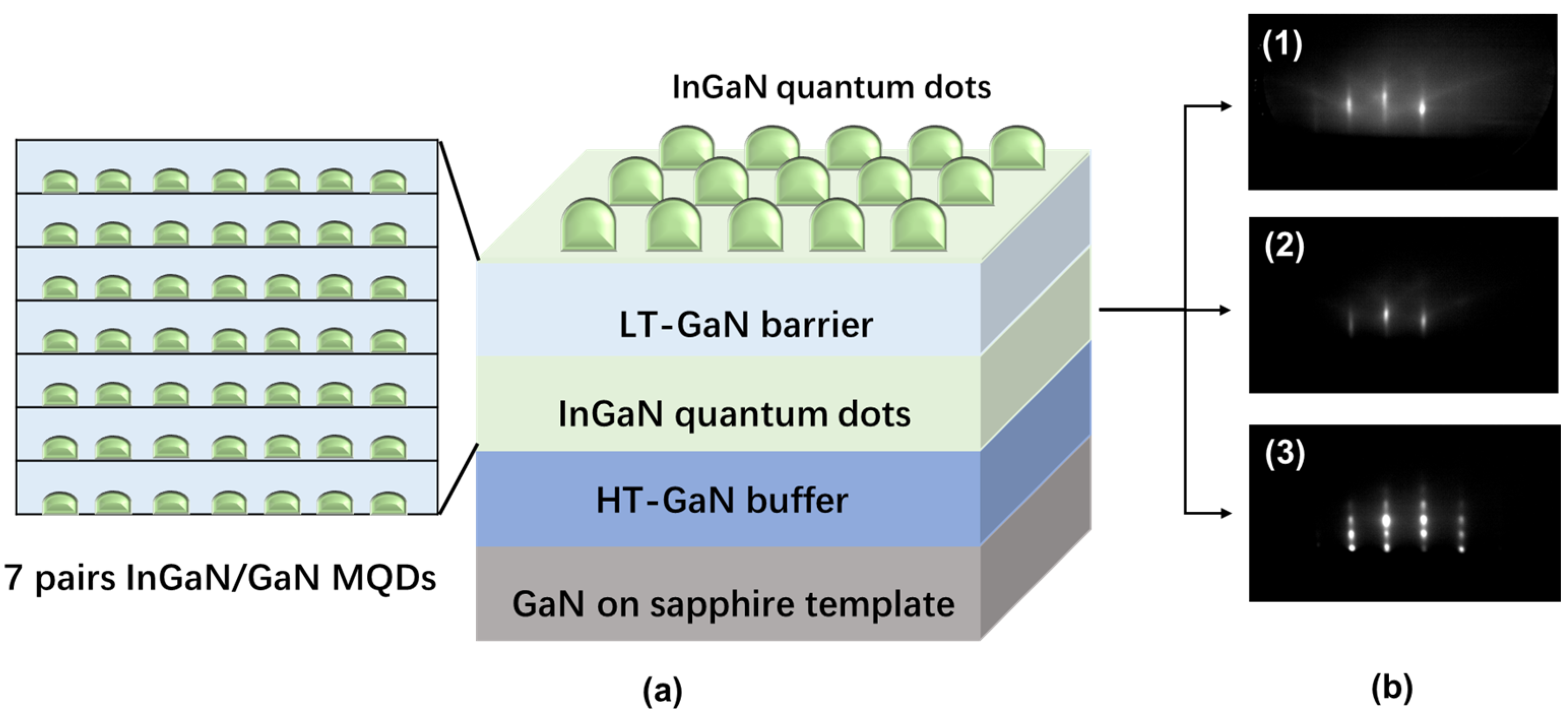
2.1. Growth of InGaN MQDs Structure

InGaN/GaN MDQs sample was epitaxially grown using Veeco Gen20A plasma-assisted molecular beam epitaxy (PA-MBE) on a c-plane (0001) 3.5-μm thick GaN-on-sapphire template. Gallium (Ga) and indium (In) are ultra-high purity solid-state single substances. Reflection high energy electron diffraction (RHEED) was used to in-situ monitor growth modes of InGaN QDs. The schematic of the sample structure is shown in Figure 1a, mainly including 8 pairs of InGaN/GaN quantum dots (QDs), and low-temperature (LT) GaN layers as quantum barriers. The top layer is a InGaN QDs material that is able to characterize their surface topography. Before growth, the GaN-on-sapphire template was cleaned using standard solvents and degassed in two steps at 200 °C for 2 h in the Load-lock chamber and at 760 °C for 0.5 h in the growth chamber to remove surface contamination and oxide film. A 100-nm thick GaN buffer layer was firstly grown at 740 °C with Ga flux in beam equivalent pressure (BEP) of 6.0 × 10⁻⁸ torr during which the RHEED pattern remined bright and streaky. InGaN QDs were grown at 630 °C with In flux of 8.0 × 10⁻⁹ torr and Ga flux of 2.0 × 10⁻⁹ torr, followed by a GaN barrier layer grown at 650 °C with Ga flux of 4.0 × 10⁻⁸ torr. The formation of QDs was proved by monitoring 2D-3D morphological transformation through RHEED from streak to spot, as shown in Figure 1b. During the growth progress, the nitrogen flow rate and plasma power were fixed at 0.6 sccm and 310 W, respectively.

2.2. Measurements of Micromorphology and Optical Properties

The surface morphology of the sample was measured by Bruker Dimension ICON AFM. The cross-sectional structure of the sample was observed using a FEI Talos F200X TEM and multilayer interface structure was measured by D8 XRD. Temperature-dependence PL spectra were measured in a range from 10 K to 300 K by tunable Ti-sapphire lasers with an excitation wavelength of 405 nm. TRPL measurements were performed using a 405 nm Ti-sapphire laser with a pulse width of 100 fs and a repetition frequency of 80 MHz, detected with a Hamamatsu C4334-04 synchro scan streak camera with a time resolution of 15 ps.

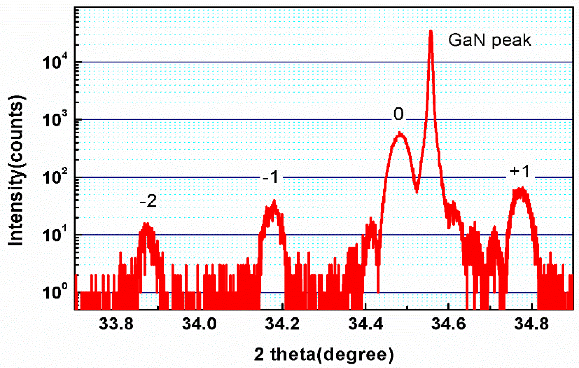
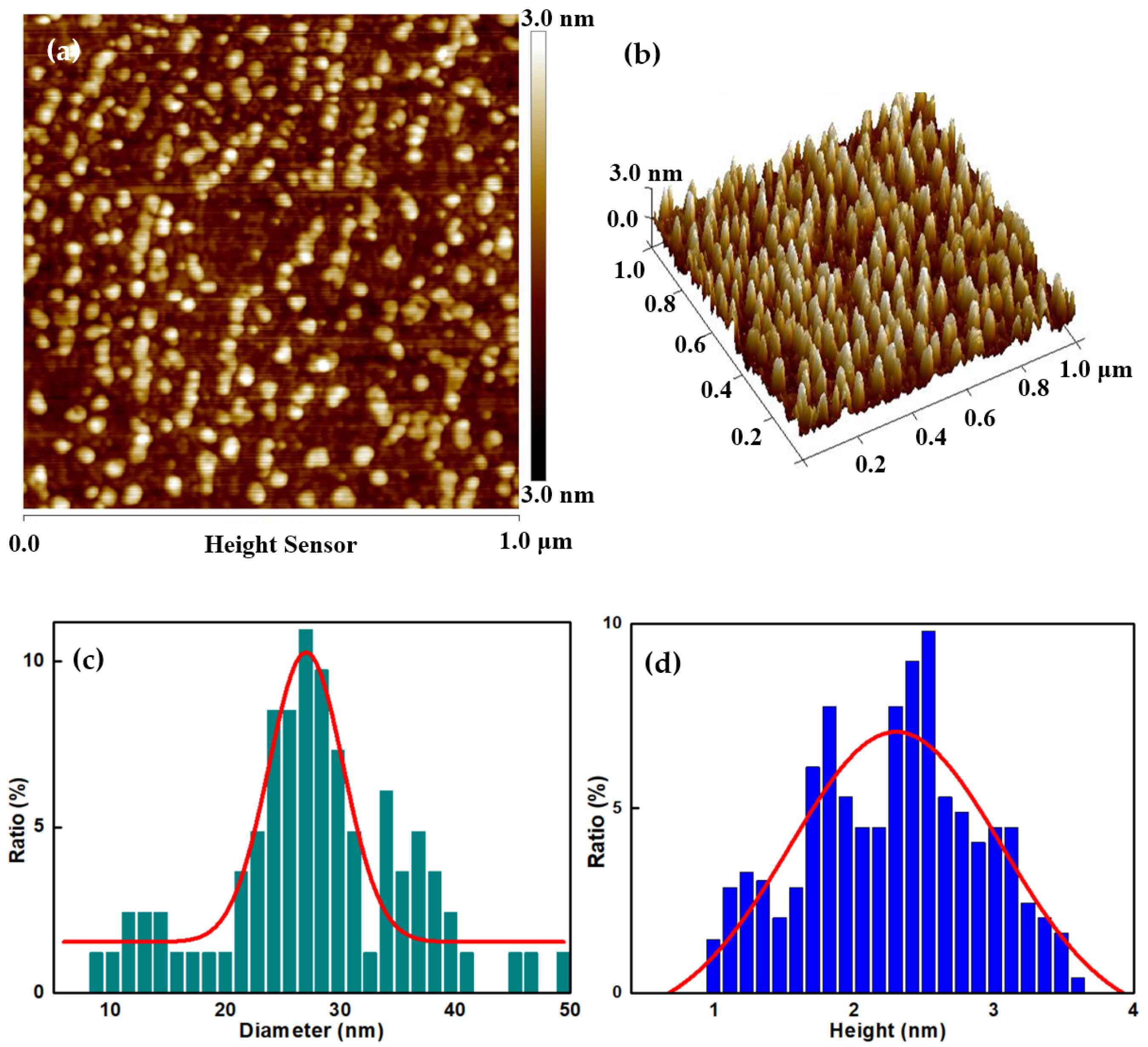
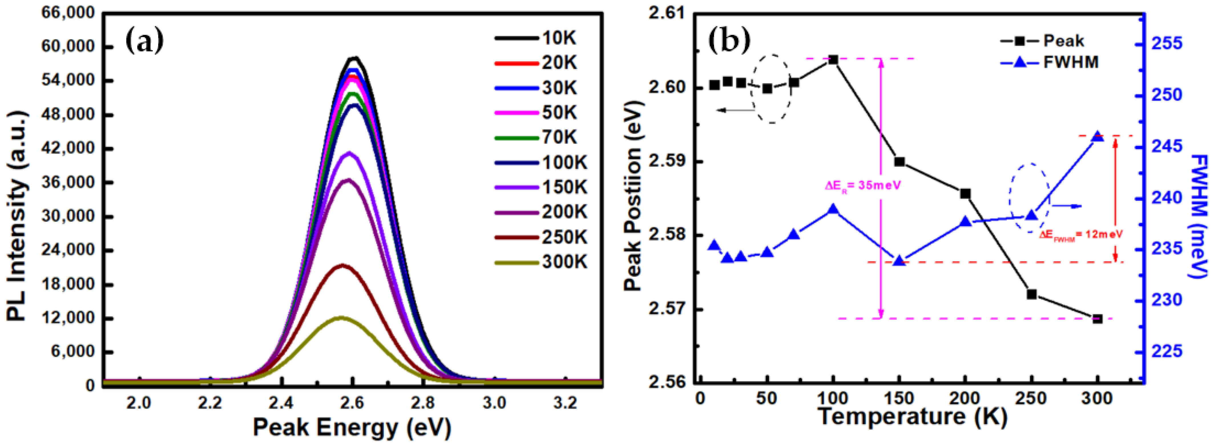
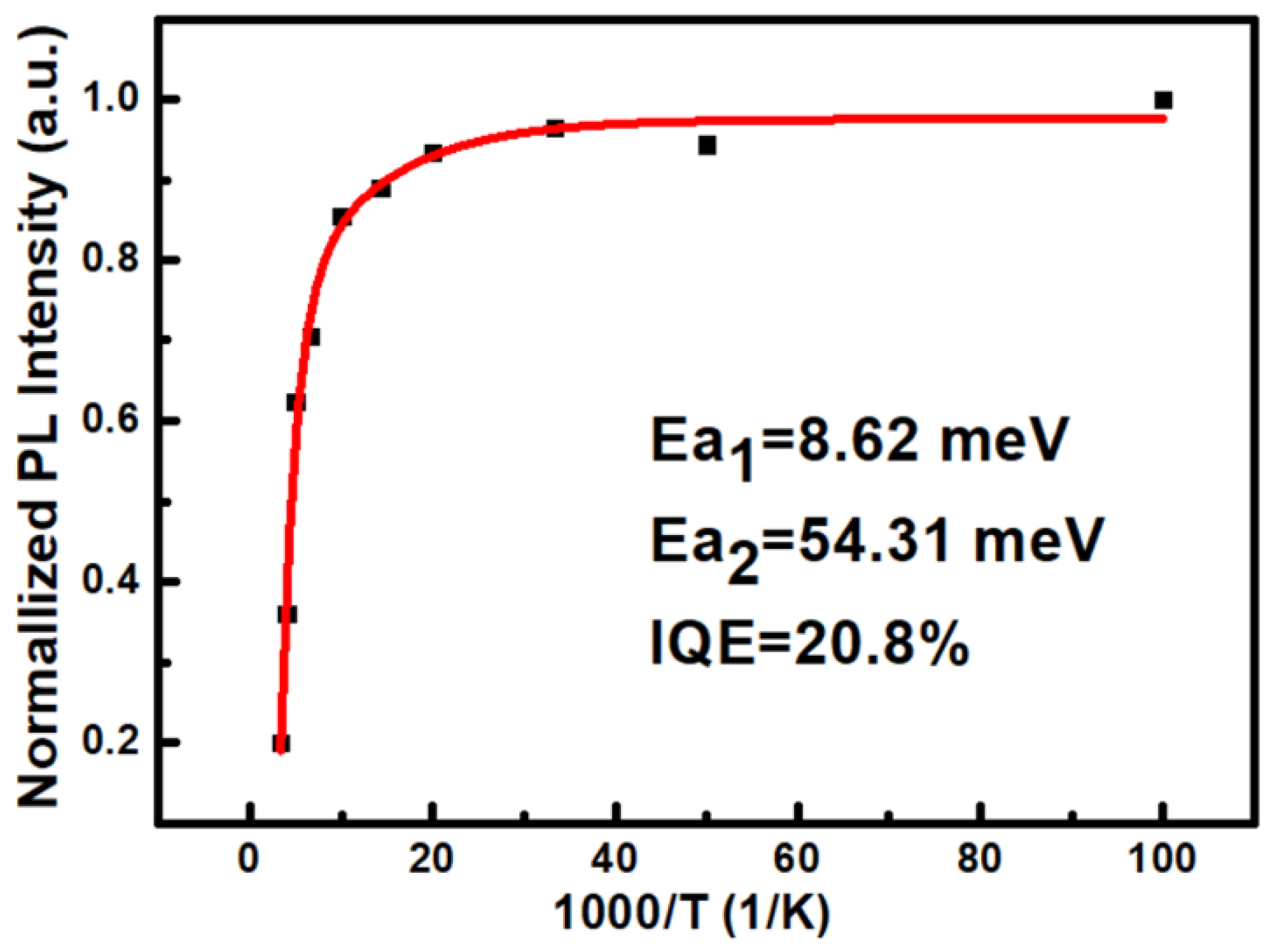
3. Results and Discussion

Figure 2 shows a high resolution XRD scan curve in (002) crystal plane of InGaN/GaN MQDs. The first and second order satellite peaks around the main reflection can be observed, which suggests that abrupt InGaN/GaN interfaces are formed. This is consistent with the phenomenon that RHEED maintains sharp and streaky patterns during the growth process of GaN barriers shown in Figure 1b, which is indicative of a two-dimensional growth model. Smooth surface morphology of GaN barriers is important for the multilayer growth of InGaN QDs and optical properties of related devices.
The surface morphology of the InGaN QDs sample was investigated by AFM under a 1 μm × 1 μm scan region as presented in Figure 3a and its three-dimensional (3-D) image is shown in Figure 3b. The truncated pyramidal feature of self-assembled QDs structure with excellent independence are exhibited and its surface density is calculated to be 3.8 × 1010 cm−2, which is similar or larger than that in other reports about InGaN QDs [19,22,23]. Figure 3c,d are the histograms of the quantum dot height and diameter size distribution, and the average of the height and diameter sizes are mainly concentrated in 2.3 ± 0.3 nm and 28 ± 4 nm, indicating distribution uniformity of dot size.
Cross-sectional TEM image and EDS mapping for In atoms of the InGaN MQDs sample are shown in Figure 4a,b respectively. The InGaN/GaN MQDs structure can be clearly observed and distinct InGaN QDs are scattered in GaN barrier layers. Figure 4c measured by HRTEM shows the enlarged partial view for InGaN QD on the surface layer. The height and diameter of the QD is estimated to be about 2.8 nm and 31 nm, respectively, which is close to the AFM results. Moreover, a coherent and abrupt InGaN/GaN QD interface without misfit dislocations can be observed, implying fully stress relaxation though 3D QD formation. The uniform size should be attributed to the GaN barrier grown under a relatively low temperature at 650 °C by MBE, which prevents the dissolution of InGaN QDs.

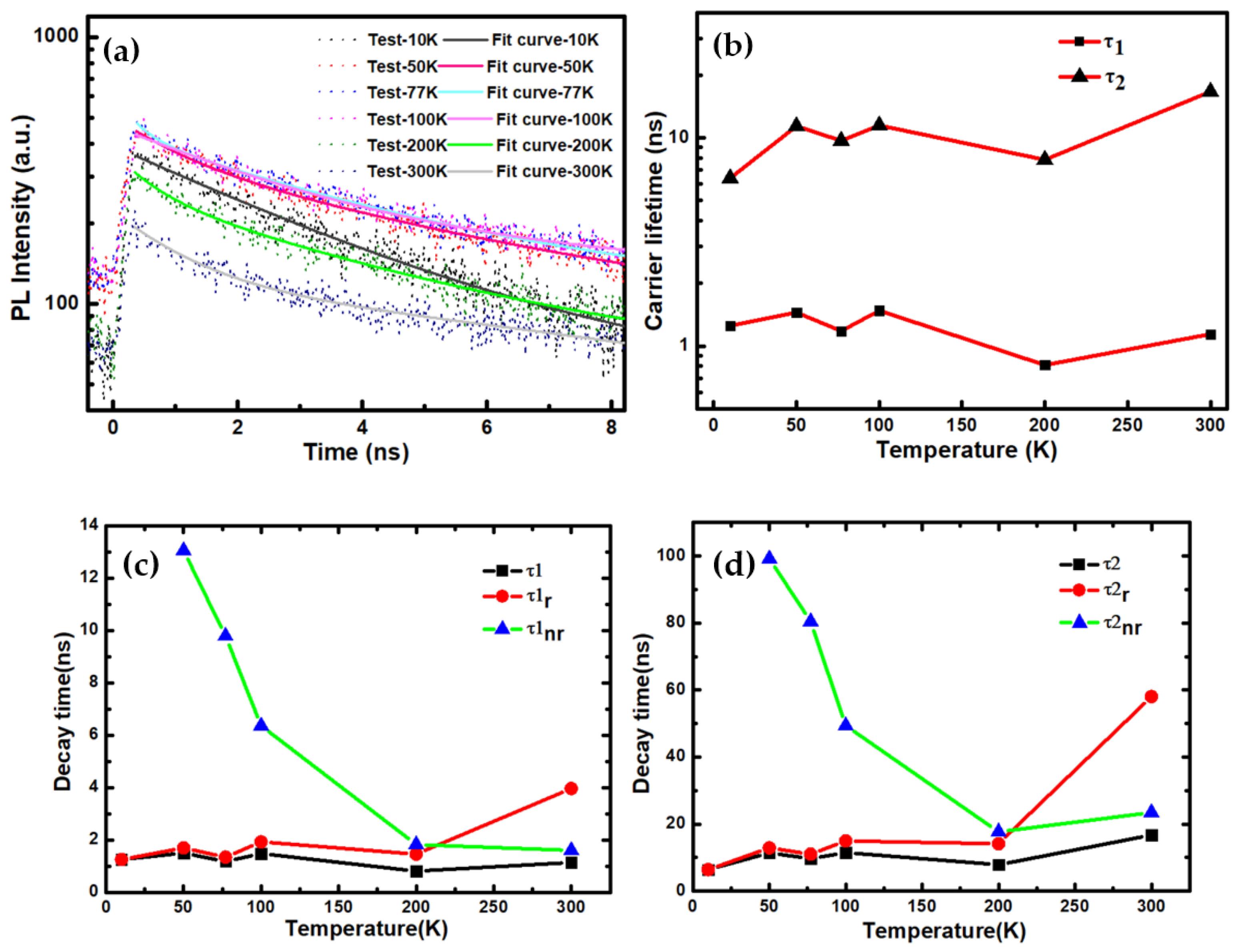
Carrier Recombination Dynamics of InGaN/GaN MQDs

The PL spectra of InGaN QDs at different temperatures from 10 K to 300 K under an excitation power of 1 mW are shown in Figure 5a. A 405-nm laser was used as an excitation source to avoid stimulating the carriers in the GaN barriers. The evolution trends of peak energy and FWHM with temperature are shown in Figure 5b. The PL peak energy remains almost unchanged in the range of 10~100 K and then exhibits a slight red-shift of 35 meV up to 300 K, which does not conform to the S-shaped behavior with the increase of temperature in both InGaN QWs and QDs [19,24,25]. At a low temperature of 10 K, carriers are randomly distributed in both shallow and deep localized states, which are caused by size and indium composition nonuniformity of QDs. The redshift of emission is commonly observed as the temperature rises slightly because the shallow localized carriers would be activated and relax into the deep localization states. However, a negligible blue-shift rather than red-shift is observed in the range of temperature lower than 100 K. It indicates that the as-grown InGaN QDs sample has a strong confinement effect even in shallow localization states, which prevents carriers from relaxing to the deep localization states. The slight blue-shift is attributed to more dispersed distribution in deep localization at a higher temperature, where the carriers are thermally activated and recombined at higher energy states. As the temperature further increases to 300 K, the carriers will escape from the localization states, and temperature-induced bandgap shrinkage effect results in a red shift of peak energy [26]. In addition, with the evolution of PL peak energy caused by the transfer and redistribution of activated carriers at different localization states, FWHM has a small increase of 12 meV from 10 K to 300 K.
The PL intensity decrease monotonically with an increasing temperature, which is due to an enhanced non-radiative recombination. Figure 6 presents the variation of normalized integrated PL intensity with temperature. The IQE is calculated to be 20.8% by an I(300 K)/I(10 K) ratio assuming that the non-radiative recombination centers are completely frozen at 10 K. The variation of normalized integrated PL intensity with temperature could be well fitted to the following Arrhenius equation [27,28],
I ( T ) = I 0 1 + α 1 exp ( E a 1 k B T ) + α 2 exp ( E a 2 k B T )
where I(T) represents the normalized integrated PL intensity at temperature T. α1 and α2 are two coefficients corresponding to the density of two kinds of non-radiative recombination centers in the samples; Ea1 and Ea2 are the activation energy related to the non-radiative recombination process. According to the fitting result, Ea1 and Ea2 are 8.62 meV and 54.31 meV, respectively. Ea1 can be regarded as the activation energy of local state centers and it may correspond to the energy of carriers being thermally activated from the band edge. Ea2 represents the necessary energy for the carrier to thermal escape from defect-related nonradiative recombination centers [14]. The values of Ea1 and Ea2 are equal or superior to the reported results. It is noted that α1 and α2 are only 4.43 and 0.34, which are much smaller than that of InGaN QWs or QDs materials grown by MOCVD [29,30]. It is proved that the as-grown InGaN QDs grown by MBE has a lower dislocation density and hence fewer non-radiative recombination centers, resulting in high IQE.
The carrier’s lifetime and transport process are critical to the device performance of LED, which are determined by the carrier’s recombination dynamics. In order to further explore the relaxation and recombination mechanism of carriers in QDs, TRPL measurements were performed at different temperatures with an excitation power of 1 mW. Figure 7a shows the TRPL decay curves at different temperatures from 10 K to 300 K. All decay curves are well fitted with a two-componential exponential function as followed [18]:
I ( t ) = A 1 exp ( t / τ 1 ) + A 2 exp ( t / τ 2 )
where I(t) is the PL intensity as a function of time, A1 and A2 are weighting coefficients, and τ1 and τ2 represent PL decay times in the fast and slow component, respectively. The fitting results of τ1 and τ2 are listed in Table 1. The decay mechanism was investigated on the basis of the presence of multiple carrier localization states. Besides two kinds of non-radiative recombination centers caused by defects according to previous analysis, there exist different QD-related localization states because of size and composition fluctuations in self-assembled InGaN QDs, which are conducive to radiative recombination. At the early-stage decay, the excited carriers in the shallow localization states recombine rapidly, and are activated by thermal energy, easily relaxing to deep localization states or nonradiative centers, which results in a fast decay process. After that, the carriers in deep localized centers need a longer time to recombine due to stronger localization effects, corresponding to slow decay process. The fitting results for τ1 and τ2 are 1.14 ns and 16.7 ns at room temperature, respectively.
As shown in Figure 7b, the PL decay times for τ1 and τ2 have similar trends and both exhibit a negligible shift as temperature increases from 10 K to 300 K. The carrier recombination dynamics in InGaN QDs can be studied by a comprehensive analysis of the temperature dependence of the PL decay time and the integrated PL intensity. The relationship between measured PL decay times τ and the radiative recombination times τr as well as the non-radiative recombination times τnr can be described as [31,32],
1 τ ( T ) = 1 τ r ( T ) + 1 τ nr ( T )
Moreover, the temperature dependence of integrated PL intensity I(T) follows the formulation,
I ( T ) = I 0 τ ( T ) τ r ( T )
where I0 is PL intensity at T = 0 K, and can be used the value of the PL intensity at 10 K. Radiative and non-radiative recombination times can be calculated by,
τ r ( T ) = I ( 10 K ) I ( T ) τ ( T )
τ nr ( T ) = I ( 10 K ) I ( 10 K ) I ( T ) τ ( T )
The calculation results of the radiative and the nonradiative recombination time as a function of temperature are shown in Figure 7c,d. For both fast and slow decay stages, τr remains almost constant at T ≤ 200 K, which is consistent with the theory that the radiative recombination time is proportional to TDx/2, where Dx is the dimension of the material, while QD material is a zero-dimension structure. The increase of τr at room temperature is attributed to the enhancement of the delocalization effect. The nonradiative lifetimes τnr decrease and become comparable to the radiative lifetime at about 200 K, mainly because more nonradiative recombination centers are thermal activated with an increasing temperature. However the total carrier lifetimes still show an increased tendency at temperature of above 200 K, so it is convincing to consider that radiative recombination dominates the recombination process due to a low dislocation density and hence high crystal quality of a QDs structure at room temperature. In addition, the ratio of A1 and A2 represented in Table 1 remains less than 1:1, although the value has a significant increase from 10 K to 300 K. It means that a majority of carriers would recombine in the deep localization states, which is beneficial for high radiation efficiency and enhanced emission for InGaN QDs-based optical devices.

4. Conclusions

In this study, we investigated micromorphology and carrier recombination dynamics of self-assembled InGaN/GaN MQDs grown by MBE on a c-plane GaN-on-sapphire template. InGaN QDs showed excellent independence with a high density of 3.8 × 1010 cm−2, with the height and diameter of dots being mainly concentrated in 2.3 nm and 28 nm, respectively. Temperature-dependence PL measurements reveal that as-grown InGaN QDs grown by MBE had a strong localization effect and low-density nonradiative recombination centers. Thus, high quality QDs with high density and uniformity resulted in a relatively high IQE of 20.8%. In addition, it was demonstrated that radiative recombination dominated the recombination process in InGaN/GaN MQDs. The two-stage decay process of TRPL decay curves was attributed to the recombination and redistribution of carriers in multiple localization states.

Author Contributions

Conceptualization and methodology, X.Z. and W.Y.; formal analysis and visu-alization, Z.X., H.Q. (Haibing Qiu), Y.S., S.K., Y.M., S.I. and Y.N.; investigation, Y.G.; writing original draft preparation, X.Z.; writing review and editing, W.Y.; supervision, H.Q. (Hua Qin) and A.T.; project administration, Y.C.; funding acquisition, S.L. and L.B. All authors have read and agreed to the published version of the manuscript.

Funding

Key R&D Program of Jiangsu Province (Grant No. BE2018005), National Natural Science Foundation of China (Grant Nos. 61875224, 61827823), the project was supported by the Guangxi Key Laboratory of Precision Navigation Technology and Application, the Guilin University of Electronic Technology (No. DH202011), SINANO (Y8AAQ21001), and the Vacuum Interconnected Nanotech Workstation (Nano-X, No. B2006).

Data Availability Statement

The data presented in this study are available within the manuscript.

Acknowledgments

The authors thank Platform for Characterization & Test, the Vacuum Interconnected Nanotech Workstation of Suzhou Institute of Nano-Tech and Nano-Bionics (SINANO), and the Chinese Academy of Sciences (CAS) for their technical support.

Conflicts of Interest

The authors declare no conflict of interest.

References

  1. DenBaars, P.S.; Feezell, D.; Kelchner, K.; Pimputkar, S.; Pan, C.; Yen, C.; Tanaka, S.; Zhao, Y.; Pfaff, N.; Farrell, R.; et al. Development of Gallium-Nitride-Based Light-Emitting Diodes (Leds) and Laser Diodes for Energy-Efficient Lighting and Displays. Acta Mater. 2013, 61, 945–951. [Google Scholar] [CrossRef]
  2. Jansen, M.; Carey, G.P.; Carico, R.; Dato, R.; Earman, A.M.; Finander, M.J.; Giaretta, G.; Hallstein, S.; Hofler, H.J.S.; Kocot, C.P.; et al. Visible laser sources for projection displays. Proj. Disp. XII 2007, 6489, 648908. [Google Scholar] [CrossRef]
  3. Mukai, T.; Nagahama, S.; Kozaki, T.; Sano, M.; Morita, D.; Yanamoto, T.; Yamamoto, M.; Akashi, K.; Masui, S. Current Status and Future Prospects of Gan-Based Leds and Lds. Phys. Stat. Sol. 2004, 201, 2712–2716. [Google Scholar] [CrossRef]
  4. Nakamura, S.; Senoh, M.; Nagahama, S.; Iwasa, N.; Yamada, T.; Matsushita, T.; Sugimoto, Y.; Kiyoku, H. Room-Temperature Continuous-Wave Operation of InGaN Multi-Quantum-Well Structure Laser Diodes. Appl. Phys. Lett. 1996, 69, 4056–4058. [Google Scholar] [CrossRef]
  5. Wu, T.; Sher, C.-W.; Lin, Y.; Lee, C.-F.; Liang, S.; Lu, Y.; Chen, S.-W.H.; Guo, W.; Kuo, H.-C.; Chen, Z. Mini-LED and Micro-LED: Promising Candidates for the Next Generation Display Technology. Appl. Sci. 2018, 8, 1557. [Google Scholar] [CrossRef] [Green Version]
  6. Nippert, F.; Karpov, S.Y.; Callsen, G.; Galler, B.; Kure, T.; Nenstiel, C.; Wagner, M.R.; Straßburg, M.; Lugauer, H.-J.; Hoffmann, A. Temperature-Dependent Recombination Coefficients in InGaN Light-Emitting Diodes: Hole Localization, Auger Processes, and the Green Gap. Appl. Phys. Lett. 2016, 109, 161103. [Google Scholar] [CrossRef] [Green Version]
  7. Saito, S.; Hashimoto, R.; Hwang, J.; Nunoue, S. InGaN Light-Emitting Diodes On c-Face Sapphire Substrates in Green Gap Spectral Range. Appl. Phys. Express 2013, 6, 111004. [Google Scholar] [CrossRef]
  8. Romanov, A.E.; Baker, T.J.; Nakamura, S.; Speck, J.S. Strain-Induced Polarization in Wurtzite Ⅲ-Nitride Semipolar Layers. J. Appl. Phys. 2006, 100, 023522. [Google Scholar] [CrossRef] [Green Version]
  9. Cho, H.K.; Lee, J.Y.; Kim, C.S.; Yang, G.M. Influence of strain relaxation on structural and optical characteristics of InGaN/GaN multiple quantum wells with high indium composition. J. Appl. Phys. 2002, 91, 1166–1170. [Google Scholar] [CrossRef]
  10. Yang, D.; Wang, L.; Hao, Z.-B.; Luo, Y.; Sun, C.; Han, Y.; Xiong, B.; Wang, J.; Li, H. Dislocation analysis of InGaN/GaN quantum dots grown by metal organic chemical vapor deposition. Superlattices Microstruct. 2016, 99, 221–225. [Google Scholar] [CrossRef]
  11. Zhao, W.; Wang, L.; Lv, W.; Wang, L.; Wang, J.; Hao, Z.; Luo, Y. Growth Behavior of High-Indium-Composition InGaN Quantum Dots Using Growth Interruption Method. Jpn. J. Appl. Phys. 2011, 50, 065601. [Google Scholar] [CrossRef]
  12. Zhang, M.; Bhattacharya, P.; Guo, W. InGaN/GaN self-organized quantum dot green light emitting diodes with reduced efficiency droop. Appl. Phys. Lett. 2010, 97, 01103. [Google Scholar] [CrossRef]
  13. Schulz, S.; O’Reilly, E. Theory of Reduced Built-in Polarization Field in Nitride-Based Quantum Dots. Phys. Rev. B 2010, 82, 033411. [Google Scholar] [CrossRef]
  14. Ee, Y.-K.; Zhao, H.; Arif, R.A.; Jamil, M.; Tansu, N. Self-assembled InGaN quantum dots on GaN emitting at 520nm grown by metalorganic vapor-phase epitaxy. J. Cryst. Growth 2008, 310, 2320–2325. [Google Scholar] [CrossRef]
  15. Chang, S.J.; Lai, W.C.; Su, Y.K.; Chen, J.F.; Liu, C.H.; Liaw, U.H. InGaN/GaN multi quantum-well blue and green light-emitting diodes. IEEE J. Sel. Top. Quantum Electron. 2002, 8, 278–283. [Google Scholar] [CrossRef]
  16. Frost, T.; Su, G.-L.; Hazari, A.; Dallesasse, J.M.; Bhattacharya, P. Red and near-Infrared Ⅲ-Nitride Quantum Dot Lasers. IEEE J. Sel. Top. Quantum Electron. 2017, 23, 1–9. [Google Scholar] [CrossRef]
  17. Dong, H.; Qu, K.; Liang, J.; Zhang, A.; Jia, Z.; Jia, W.; Xu, B.; Liu, X.; Li, G.; Wu, Y. Evolution mechanism of InGaN quantum dots and their optical properties. Opt. Mater. 2019, 99, 109554. [Google Scholar] [CrossRef]
  18. Li, Y.; Jin, Z.; Han, Y.; Zhao, C.; Huang, J.; Tang, C.W.; Wang, J.; Lau, K.M. Surface morphology and optical properties of InGaN quantum dots with varying growth interruption time. Mater. Res. Express 2019, 7, 015903. [Google Scholar] [CrossRef]
  19. Weng, G.-E.; Zhao, W.-R.; Chen, S.-Q.; Akiyama, H.; Li, Z.-C.; Liu, J.-P.; Zhang, B.-P. Strong localization effect and carrier relaxation dynamics in self-assembled InGaN quantum dots emitting in the green. Nanoscale Res. Lett. 2015, 10, 31. [Google Scholar] [CrossRef] [Green Version]
  20. Wang, L.; Wang, L.; Yu, J.D.; Hao, Z.B.; Luo, Y.; Sun, C.Z.; Han, Y.J.; Xiong, B.; Wang, J.; Li, H.T. Abnormal Stranski-Krastanov Mode Growth of Green InGaN Quantum Dots: Morphology, Optical Properties, and Applications in Light-Emitting Devices. ACS Appl. Mater. Interfaces 2019, 11, 1228–1238. [Google Scholar] [CrossRef]
  21. Yao, H.H.; Lu, T.-C.; Huang, G.S.; Chen, C.Y.; Liang, W.D.; Kuo, H.C.; Wang, S.C. InGaN self-assembled quantum dots grown by metal–organic chemical vapour deposition with growth interruption. Nanotechnology 2006, 17, 1713–1716. [Google Scholar] [CrossRef]
  22. Reilly, C.E.; Bonef, B.; Nakamura, S.; Speck, J.S.; Denbaars, S.; Keller, S. Characterization of InGaN quantum dots grown by metalorganic chemical vapor deposition. Semicond. Sci. Technol. 2019, 34, 125002. [Google Scholar] [CrossRef]
  23. Li, H.; Li, P.; Kang, J.; Ding, J.; Ma, J.; Zhang, Y.; Yi, X.; Wang, G. Broadband full-color monolithic InGaN light-emitting diodes by self-assembled InGaN quantum dots. Sci. Rep. 2016, 6, 35217. [Google Scholar] [CrossRef]
  24. Zhao, C.; Tang, C.W.; Lai, B.; Cheng, G.; Wang, J.; Lau, K.M. Low-Efficiency-Droop InGaN Quantum Dot Light-Emitting Diodes Operating in the “Green Gap”. Photonics Res. 2020, 8, 750–754. [Google Scholar] [CrossRef]
  25. Xing, Y.; Zhao, D.; Jiang, D.; Liu, Z.; Zhu, J.; Chen, P.; Yang, J.; Liang, F.; Liu, S.; Zhang, L. Carrier Redistribution Between Two Kinds of Localized States in the InGaN/GaN Quantum Wells Studied by Photoluminescence. Nanoscale Res. Lett. 2019, 14, 88. [Google Scholar] [CrossRef] [PubMed]
  26. Sun, G.; Xu, G.B.; Ding, Y.J.; Zhao, H.P.; Liu, G.Y.; Zhang, J.; Tansu, N. Investigation of Fast and Slow Decays in InGaN/GaN Quantum Wells. Appl. Phys. Lett. 2011, 99, 081104. [Google Scholar] [CrossRef] [Green Version]
  27. Mohanta, A.; Jang, D.J.; Wang, M.S.; Tu, L.W. Time-Integrated Photoluminescence and Pump-Probe Reflection Spectroscopy of Si Doped Inn Thin Films. J. Appl. Phys. 2014, 115, 044906. [Google Scholar] [CrossRef]
  28. Li, T.; Fischer, A.M.; Wei, Q.Y.; Ponce, F.A.; Detchprohm, T.; Wetzel, C. Carrier Localization and Nonradiative Recombination in Yellow Emitting InGaN Quantum Wells. Appl. Phys. Lett. 2010, 96, 031906. [Google Scholar] [CrossRef] [Green Version]
  29. Liu, J.; Jia, Z.; Ma, S.; Dong, H.; Zhai, G.; Xu, B. Enhancement of carrier localization effect and internal quantum efficiency through In-rich InGaN quantum dots. Superlattices Microstruct. 2018, 113, 497–501. [Google Scholar] [CrossRef]
  30. Tian, A.; Liu, J.; Zhang, L.; Ikeda, M.; Fan, X.; Zhang, S.; Li, D.; Zhang, F.; Wen, P.; Cheng, Y.; et al. Optical characterization of InGaN/GaN quantum well active region of green laser diodes. Appl. Phys. Express 2016, 10, 12701. [Google Scholar] [CrossRef]
  31. Chichibu, S.; Onuma, T.; Sota, T.; DenBaars, S.P.; Nakamura, S.; Kitamura, T.; Ishida, Y.; Okumura, H. Influence of InN Mole Fraction on the Recombination Processes of Localized Excitons in Strained Cubic InxGa1-XN/Gan Multiple Quantum Wells. J. Appl. Phys. 2003, 93, 2051–2054. [Google Scholar] [CrossRef]
  32. Minsky, M.S.; Watanabe, S.; Yamada, N. Radiative and nonradiative lifetimes in GaInN/GaN multiquantum wells. J. Appl. Phys. 2002, 91, 5176–5181. [Google Scholar] [CrossRef]
Figure 1. (a)The schematic of the sample structure and (b) the evolution of RHEED pattern during the formation process of InGaN QDs.
Crystals 11 01312 g001
Figure 2. HRXRD scan curve in (002) crystal plane of a InGaN/GaN MQDs structure on a GaN template.
Crystals 11 01312 g002
Figure 3. (a) AFM image and (b) corresponding 3-D images of the surface layer for InGaN QDs at a scan region of 1 μm × 1 μm; (c) height distribution histogram of the surface layer of InGaN QDs; and (d) diameter distribution histogram of the surface layer of InGaN QDs.
Crystals 11 01312 g003
Figure 4. (a) Cross-sectional transmission electron microscopy image of InGaN MQDs and (b) two-dimensional EDS mapping for In atoms; (c) enlarged partial view of QD on the surface.
Crystals 11 01312 g004
Figure 5. (a) PL spectra of InGaN QDs sample at different temperatures from 10 K to 300 K; (b) PL peak energy and FWHM as a function of temperature.
Crystals 11 01312 g005
Figure 6. Variation of the normalized integrated PL intensity with the reciprocal temperature for the InGaN QDs sample. The red solid lines represent the Arrhenius fitting results.
Crystals 11 01312 g006
Figure 7. (a) TRPL spectra of InGaN/GaN MQDs at different temperatures and (b) the variation of PL decay times for τ1 and τ2 with temperature. Temperature dependence of the carrier recombination time for (c) τ1 and (d) τ2.
Crystals 11 01312 g007
Table 1. PL decay times of fast and slow component at different temperatures.
Temperature (K)105077100200300
τ1 (ns)1.251.51.181.480.811.14
τ2 (ns)6.4111.49.711.497.8616.7
A1:A216:8441:5934:6636:6436:6448:52
Publisher’s Note: MDPI stays neutral with regard to jurisdictional claims in published maps and institutional affiliations.

