A Comparison Study on Multilayered Barrier Oxide Structure in Charge Trap Flash for Synaptic Operation


Abstract
1. Introduction
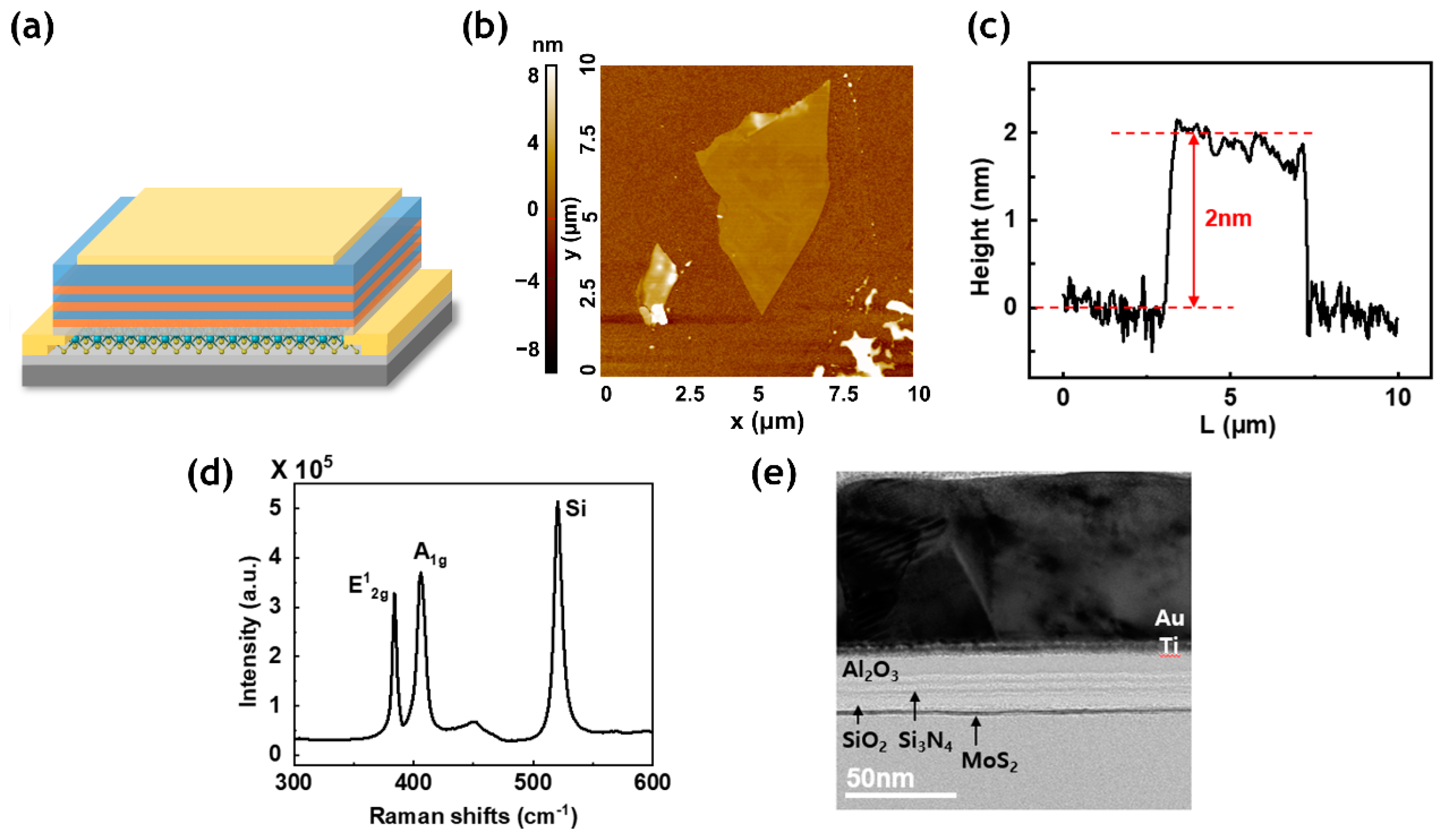
2. Fabrication Methods
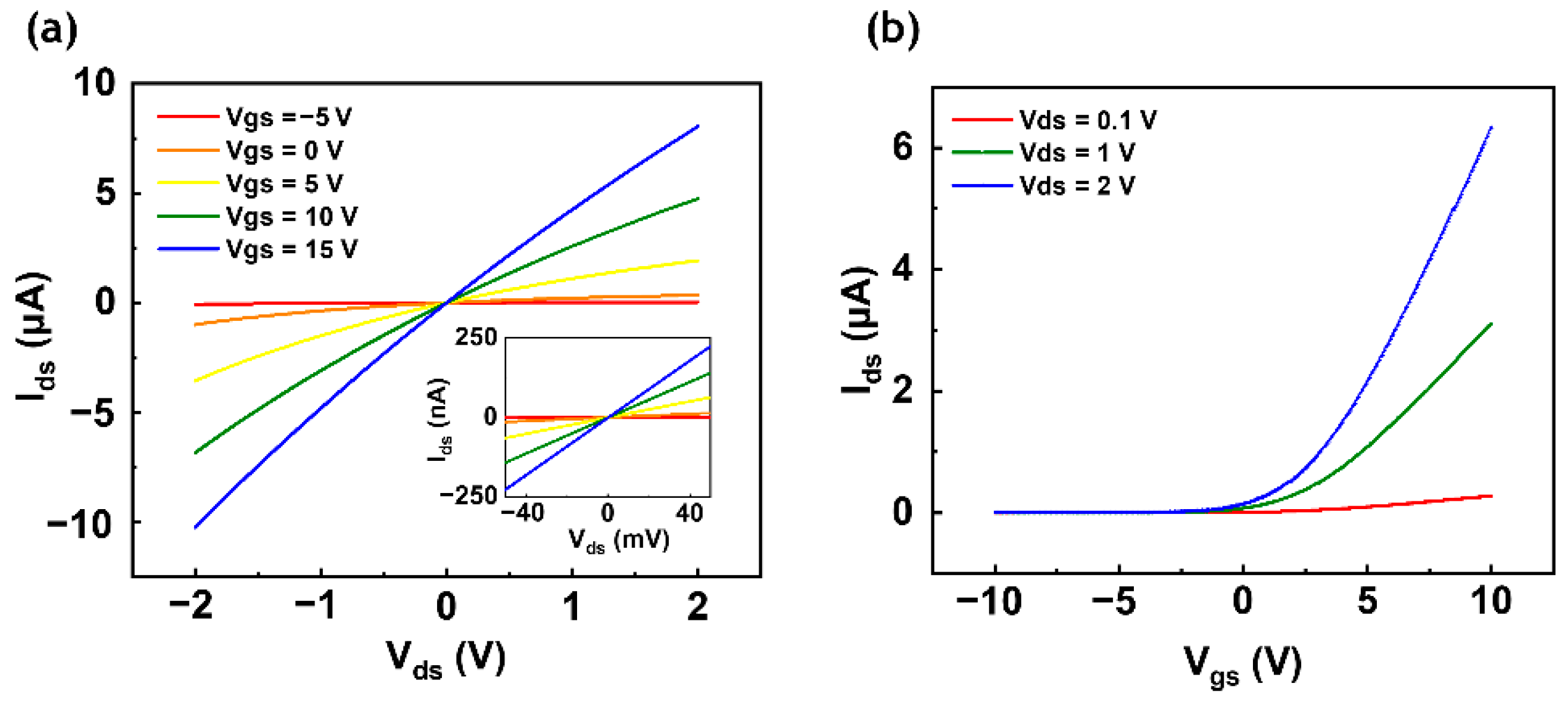
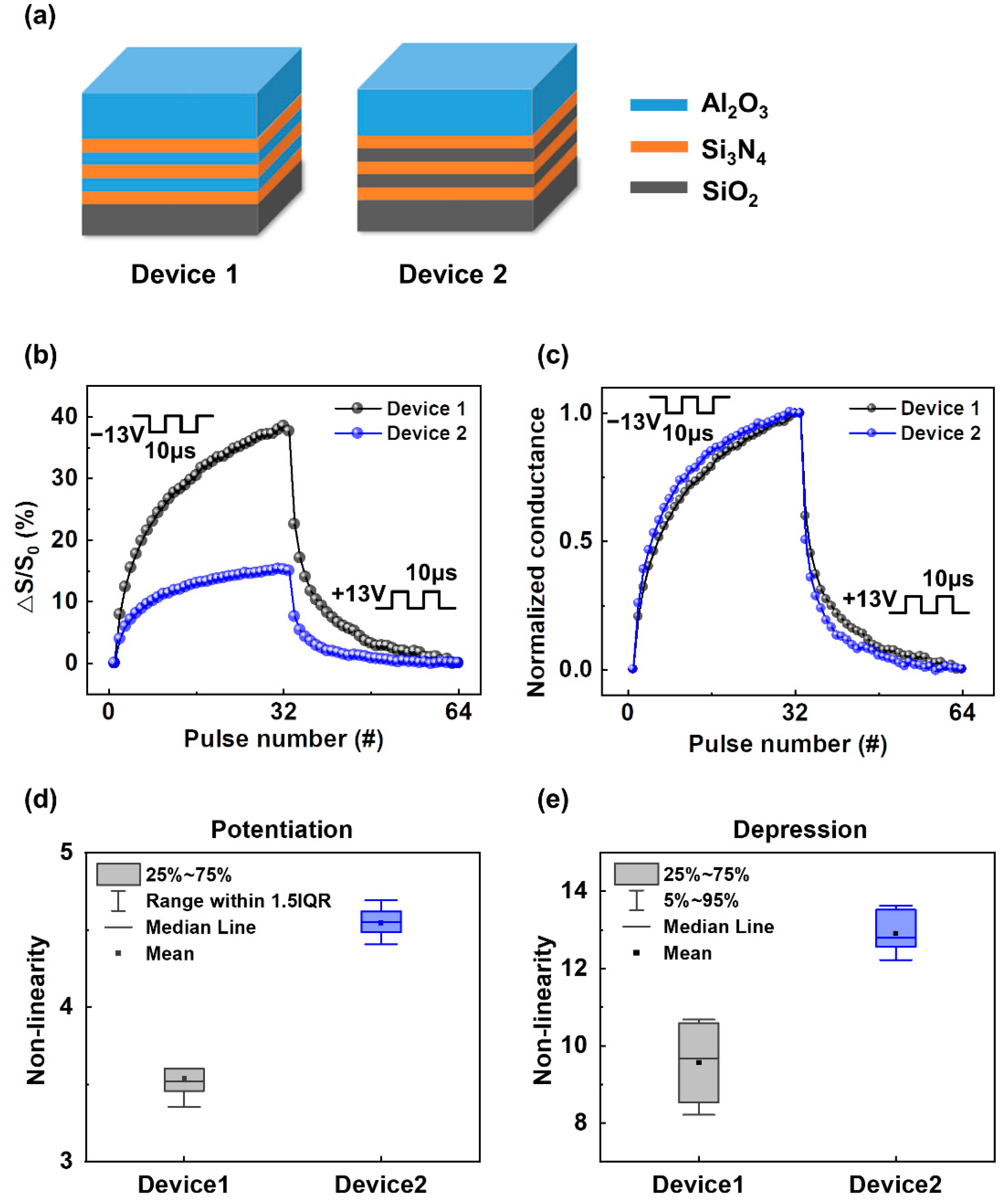
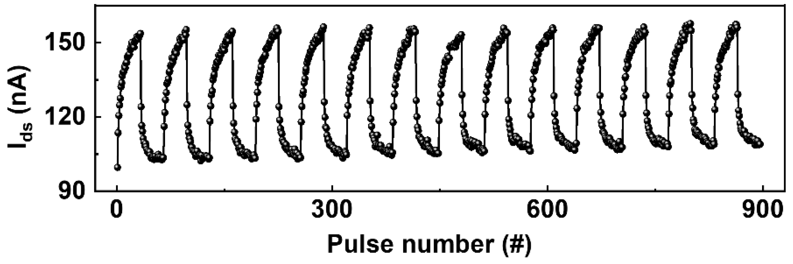
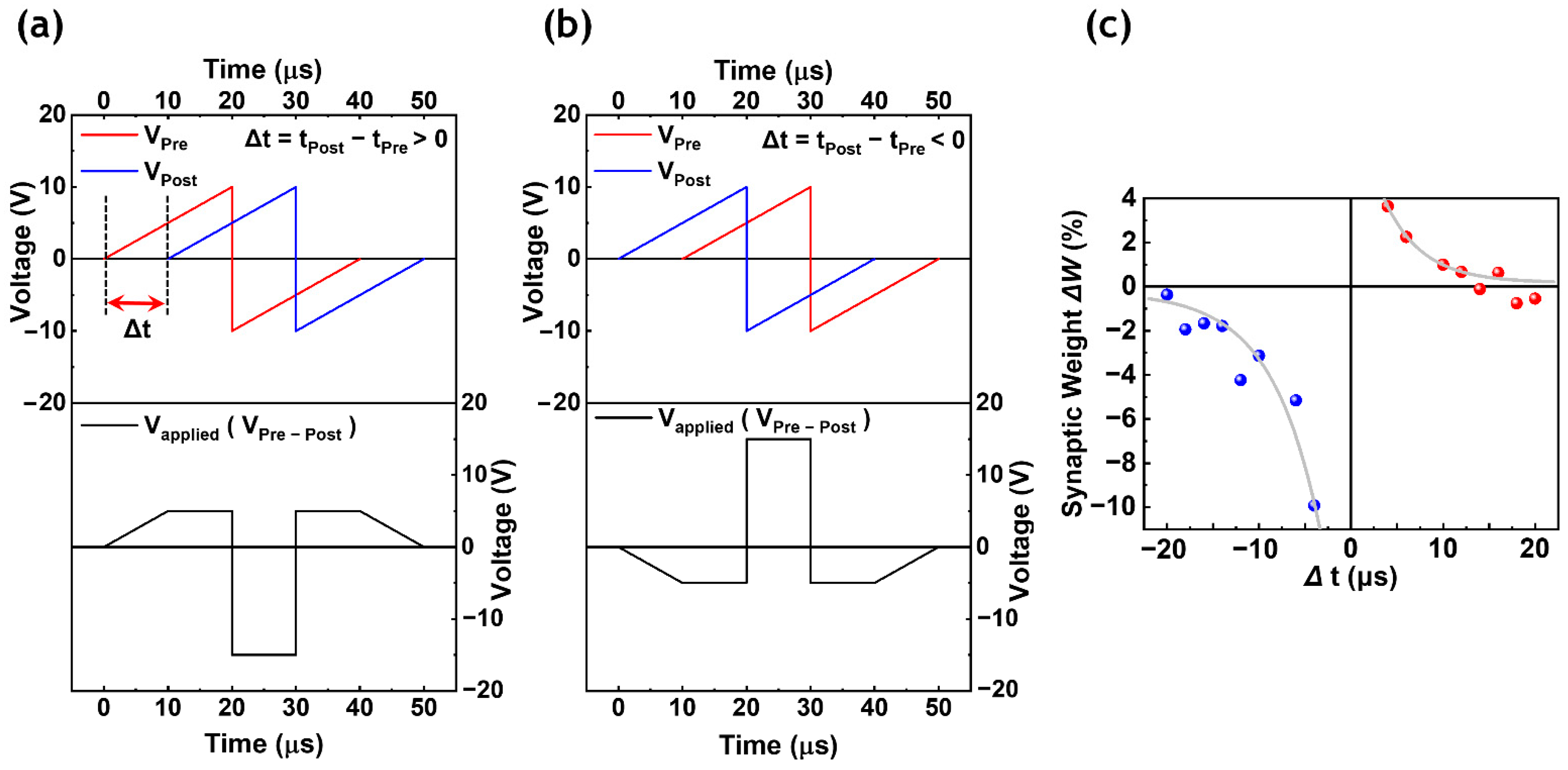
3. Results and Discussion
4. Conclusions
Author Contributions
Funding
Conflicts of Interest
References
- Nilsson, N.J. Principles of Artificial Intelligence; Morgan Kaufmann: Burlington, MA, USA, 2014. [Google Scholar]
- Mitchell, R.; Michalski, J.; Carbonell, T. An Artificial Intelligence Approach; Springer: Berlin/Heidelberg, Germany, 2013. [Google Scholar]
- Calhoun, B.H.; Wang, A.; Chandrakasan, A. Modeling and sizing for minimum energy operation in subthreshold circuits. IEEE J. Solid State Circuits 2005, 40, 1778–1786. [Google Scholar] [CrossRef]
- Hasler, J.; Marr, H.B. Finding a roadmap to achieve large neuromorphic hardware systems. Front. Neurosci. 2013, 7, 118. [Google Scholar] [CrossRef] [PubMed]
- Goelet, P.; Castellucci, V.F.; Schacher, S.; Kandel, E.R. The long and the short of long–term memory—A molecular framework. Nature 1986, 322, 419–422. [Google Scholar] [CrossRef] [PubMed]
- Striedter, G.F. Neurobiology: A Functional Approach; Oxford University Press: Oxford, UK, 2016. [Google Scholar]
- Bi, G.-q.; Poo, M.-m. Distributed synaptic modification in neural networks induced by patterned stimulation. Nature 1999, 401, 792–796. [Google Scholar] [CrossRef] [PubMed]
- Nithianantharajah, J.; Hannan, A.J. The neurobiology of brain and cognitive reserve: Mental and physical activity as modulators of brain disorders. Prog. Neurobiol. 2009, 89, 369–382. [Google Scholar] [CrossRef] [PubMed]
- Chen, P.-Y.; Peng, X.; Yu, S. NeuroSim+: An integrated device-to-algorithm framework for benchmarking synaptic devices and array architectures. In Proceedings of the 2017 IEEE International Electron Devices Meeting (IEDM), San Francisco, CA, USA, 2–6 December 2017; pp. 6.1.1–6.1.4. [Google Scholar]
- Chen, P.-Y.; Peng, X.; Yu, S. NeuroSim: A circuit-level macro model for benchmarking neuro-inspired architectures in online learning. IEEE Trans. Comput. Aided Des. Integr. Circuits Syst. 2018, 37, 3067–3080. [Google Scholar] [CrossRef]
- Jung, M.-H.; Kim, K.-S.; Park, G.-H.; Cho, W.-J. Dependence of charge trapping and tunneling on the silicon-nitride (Si3N4) thickness for tunnel barrier engineered nonvolatile memory applications. Appl. Phys. Lett. 2009, 94, 053508. [Google Scholar] [CrossRef]
- Lee, G.-H.; Cui, X.; Kim, Y.D.; Arefe, G.; Zhang, X.; Lee, C.-H.; Ye, F.; Watanabe, K.; Taniguchi, T.; Kim, P. Highly stable, dual-gated MoS2 transistors encapsulated by hexagonal boron nitride with gate-controllable contact, resistance, and threshold voltage. ACS Nano 2015, 9, 7019–7026. [Google Scholar] [CrossRef] [PubMed]
- Frindt, R. Single crystals of MoS2 several molecular layers thick. J. Appl. Phys. 1966, 37, 1928–1929. [Google Scholar] [CrossRef]
- Zheng, X.; Calò, A.; Albisetti, E.; Liu, X.; Alharbi, A.S.M.; Arefe, G.; Liu, X.; Spieser, M.; Yoo, W.J.; Taniguchi, T. Patterning metal contacts on monolayer MoS2 with vanishing Schottky barriers using thermal nanolithography. Nat. Electron. 2019, 2, 17–25. [Google Scholar] [CrossRef]
- Qian, Q.; Lei, J.; Wei, J.; Zhang, Z.; Tang, G.; Zhong, K.; Zheng, Z.; Chen, K.J. 2D materials as semiconducting gate for field-effect transistors with inherent over-voltage protection and boosted ON-current. NPJ 2D Mater. Appl. 2019, 3, 1–9. [Google Scholar] [CrossRef]
- Bertolazzi, S.; Krasnozhon, D.; Kis, A. Nonvolatile memory cells based on MoS2/graphene heterostructures. ACS Nano 2013, 7, 3246–3252. [Google Scholar] [CrossRef] [PubMed]
- Bao, W.; Cai, X.; Kim, D.; Sridhara, K.; Fuhrer, M.S. High mobility ambipolar MoS2 field-effect transistors: Substrate and dielectric effects. Appl. Phys. Lett. 2013, 102, 042104. [Google Scholar] [CrossRef]
- Sah, R.E. Silicon Nitride, Silicon Dioxide, and Emerging Dielectrics 11. In Proceedings of the 219th ECS Meeting, Montreal, Canada, 1–6 May 2011. [Google Scholar]
- Puzzilli, G.; Govoreanu, B.; Irrera, F.; Rosmeulen, M.; Van Houdt, J. Characterization of charge trapping in SiO2/Al2O3 dielectric stacks by pulsed C–V technique. Microelectron. Reliab. 2007, 47, 508–512. [Google Scholar] [CrossRef]
- Agarwal, S.; Plimpton, S.J.; Hughart, D.R.; Hsia, A.H.; Richter, I.; Cox, J.A.; James, C.D.; Marinella, M.J. Resistive memory device requirements for a neural algorithm accelerator. In Proceedings of the 2016 International Joint Conference on Neural Networks (IJCNN), Vancouver, BC, Canada, 24–29 July 2016; pp. 929–938. [Google Scholar]
- Shouval, H.Z.; Wang, S.S.-H.; Wittenberg, G.M. Spike timing dependent plasticity: A consequence of more fundamental learning rules. Front. Comput. Neurosci. 2010, 4, 19. [Google Scholar] [CrossRef]
- Xu, R.; Jang, H.; Lee, M.-H.; Amanov, D.; Cho, Y.; Kim, H.; Park, S.; Shin, H.-j.; Ham, D. Vertical MoS2 double-layer memristor with electrochemical metallization as an atomic-scale synapse with switching thresholds approaching 100 mV. Nano Lett. 2019, 19, 2411–2417. [Google Scholar] [CrossRef] [PubMed]


Publisher’s Note: MDPI stays neutral with regard to jurisdictional claims in published maps and institutional affiliations. |
© 2021 by the authors. Licensee MDPI, Basel, Switzerland. This article is an open access article distributed under the terms and conditions of the Creative Commons Attribution (CC BY) license (http://creativecommons.org/licenses/by/4.0/).
Share and Cite
Kim, M.; Park, E.; Kim, I.S.; Park, J.; Kim, J.; Jeong, Y.; Lee, S.; Kim, I.; Park, J.-K.; Seong, T.-Y.; et al. A Comparison Study on Multilayered Barrier Oxide Structure in Charge Trap Flash for Synaptic Operation. Crystals 2021, 11, 70. https://doi.org/10.3390/cryst11010070
Kim M, Park E, Kim IS, Park J, Kim J, Jeong Y, Lee S, Kim I, Park J-K, Seong T-Y, et al. A Comparison Study on Multilayered Barrier Oxide Structure in Charge Trap Flash for Synaptic Operation. Crystals. 2021; 11(1):70. https://doi.org/10.3390/cryst11010070
Chicago/Turabian StyleKim, Minkyung, Eunpyo Park, In Soo Kim, Jongkil Park, Jaewook Kim, YeonJoo Jeong, Suyoun Lee, Inho Kim, Jong-Keuk Park, Tae-Yeon Seong, and et al. 2021. "A Comparison Study on Multilayered Barrier Oxide Structure in Charge Trap Flash for Synaptic Operation" Crystals 11, no. 1: 70. https://doi.org/10.3390/cryst11010070
APA StyleKim, M., Park, E., Kim, I. S., Park, J., Kim, J., Jeong, Y., Lee, S., Kim, I., Park, J.-K., Seong, T.-Y., & Kwak, J. Y. (2021). A Comparison Study on Multilayered Barrier Oxide Structure in Charge Trap Flash for Synaptic Operation. Crystals, 11(1), 70. https://doi.org/10.3390/cryst11010070