Article

Low-Frequency Noise Behavior of AlGaN/GaN HEMTs with Different Al Compositions

1
Department of Advanced Materials Science and Engineering, Kumoh National Institute of Technology, Gumi 39177, Korea
2
Yield Enhancement Team, Foundry, Samsung Electronics Company Ltd., Yongin 17113, Korea
3
Advanced Material Research Center, Kumoh National Institute of Technology, Gumi 39177, Korea
*
Author to whom correspondence should be addressed.
Crystals 2020, 10(9), 830; https://doi.org/10.3390/cryst10090830
Submission received: 27 August 2020 / Accepted: 15 September 2020 / Published: 17 September 2020

Abstract

:
AlxGa1−xN/GaN heterostructures with two kinds of Al composition were grown by metal organic chemical vapor deposition (MOCVD) on sapphire substrates. The Al compositions in the AlGaN barrier layer were confirmed to be 13% and 28% using high resolution X-ray diffraction (HRXRD). AlxGa1−xN/GaN high-electron mobility transistors (HEMTs) with different Al compositions were fabricated, characterized, and compared using the Hall effect, direct current (DC), and low-frequency noise (LFN). The device with high Al composition (28%) showed improved sheet resistance (Rsh) due to enhanced carrier confinement and reduced gate leakage currents caused by increased Schottky barrier height (SBH). On the other hand, the reduced noise level and the low trap density (Nt) for the device of 13% of Al composition were obtained, which is attributed to the mitigated carrier density and decreased dislocation density in the AlxGa1−xN barrier layer according to the declined Al composition. In spite of the Al composition, the fabricated devices exhibited 1/ƒ noise behavior with the carrier number fluctuation (CNF) model, which is proved by the curves of both (SId/Id2) versus (gm/Id)2 and (SId/Id2) versus (Vgs–Vth). Although low Al composition is favorable to the reduced noise, it causes some problems like low Rsh and high gate leakage current. Therefore, the optimized Al composition in AlGaN/GaN HEMT is required to improve both noise and DC properties.

Graphical Abstract

1. Introduction

AlxGa1−xN/GaN high-electron mobility transistors (HEMTs) are very attractive devices for both high-power and high-temperature operations [1]. This is because the wide energy band gap (Eg) of above 3.4 eV allows for higher supply voltages and reliable device performances at high temperature [2]. In addition, spontaneous and piezoelectric polarization in the AlGaN/GaN heterostructures gives high electron densities and high transconductance (gm), which lead to having advantages for applying high-frequency and high-current devices [3,4].
Generally, when Al composition in the AlxGa1−xN barrier layer increases, the conduction band discontinuity and the polarization-induced electrons are increased, which results in high sheet carrier concentration in the two-dimensional electron gas (2DEG) located at the AlxGa1−xN/GaN heterostructure [3]. However, high Al composition makes easy to generate the dislocations in the AlxGa1−xN barrier layer due to the large lattice mismatch between the AlxGa1−xN and GaN layers caused by the discrepancy of their Eg. These dislocations play the roles of trap states and charge scattering centers, which leads to the deterioration of device performance, such as severe current collapse, increased gate leakage current, and degraded gm [4]. Therefore, in order to achieve improved device performance, it is needed to optimize the Al composition in the AlxGa1−xN barrier layer.
Low-frequency noise (LFN) measurement for AlGaN/GaN HEMTs is an efficient tool to exam device performance, analyze material defects, and study device reliability [5,6,7,8]. Many research groups have reported by investigating the effects of in situ/ex situ passivation layers [9,10], the gate-to-drain distance [7], and the types of GaN buffer layer [11] on the LFN of AlGaN/GaN HEMTs. M. D. Hasan, et al. [6] demonstrated that the AlGaN/GaN metal-oxide-semiconductor (MOS)-HEMT with Al composition of 20% exhibited a lower noise level than that of the device with Al composition of 35%. However, the noise fluctuations mechanism between the 2DEG channel and gate oxide in AlGaN/GaN MOS-HEMTs are complicated due to their double gate oxide layers: (1) the AlGaN barrier layer; (2) the deposited oxide layer. No detailed noise characterization has been performed in AlGaN/GaN HEMT according to the Al composition without oxide layer. Here, we investigate the structural and electrical characteristics of AlxGa1−xN/GaN HEMTs with two different Al compositions (x = 0.13 and 0.28) using high resolution X-ray diffraction (HRXRD), the Hall effect, direct current (DC), and LFN measurement.

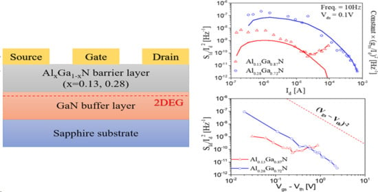
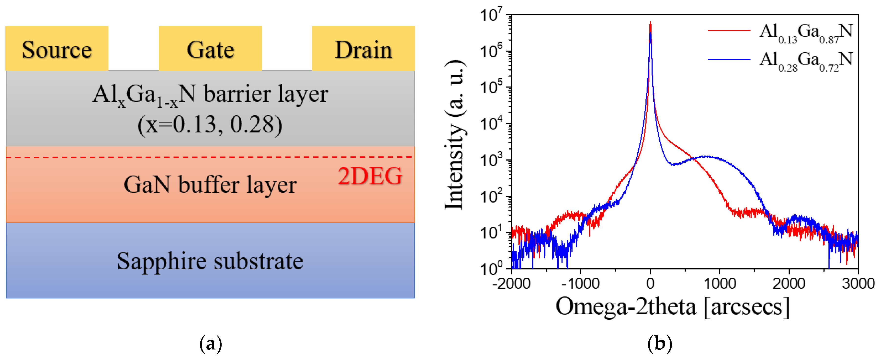
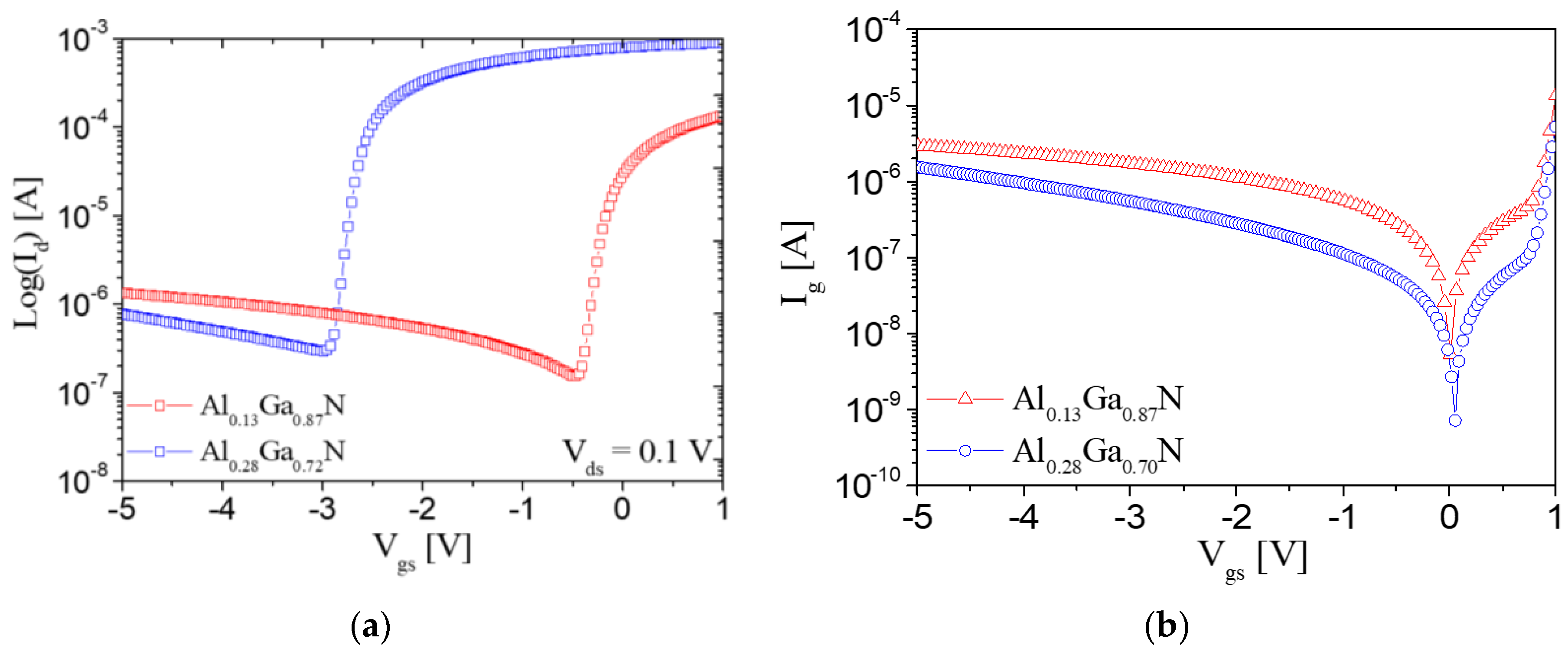
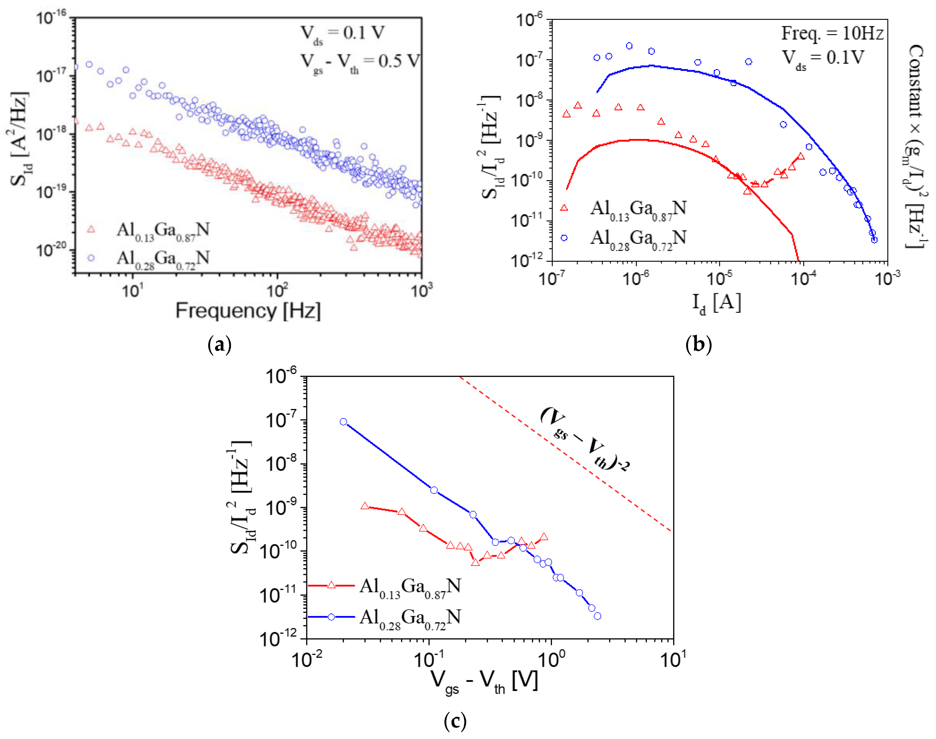
2. Materials and Methods

The AlxGa1−xN/GaN heterostructures were grown on sapphire substrates by metal organic chemical vapor deposition (MOCVD). The layer structure consisted of a 30 nm-thick GaN initial nucleation layer grown at low temperature, a 3 μm-thick highly resistive GaN buffer layer, and a AlGaN barrier layer (Figure 1a). To find the Al composition and the thickness of AlGaN, the ω-2θ scan of the diffraction plane for two samples was measured using the HRXRD in Figure 1b. The detailed Al composition and AlGaN thickness are shown in Table 1. The intensity of the GaN buffer layer was found to be sharp and high, but the AlGaN peak located near the GaN peak presented to be broad and low (Figure 1b), which means that the GaN buffer layer exhibits much better crystal quality compared with the AlGaN barrier layer. It was also noted that the AlGaN peak shifts to positive as the AlGaN composition increases. The reason for the peak shift is due to the decreased lattice constant of the AlGaN barrier layer [12], which leads to the large lattice mismatch between the thin AlGaN barrier layer and the underlying thick GaN layer. This results in generating the dislocations in the AlGaN barrier layer as the Al composition increases [13]. Hall effect measurements showed that the sheet resistance (Rsh) for the AlxGa1−xN/GaN heterostructure with x = 0.13 and 0.28 were 1923 and 421 Ω/sq, respectively (the detailed electron mobilities and 2DEG densities for all samples are depicted in Table 1). The enhancement of Rsh as a function of the Al composition is due to the improved carrier confinement and polarization in the 2DEG quantum well [3].
Device fabrication was commenced with mesa isolation by inductively coupled plasma-reactive ion etching (ICP-RIE). Ohmic contacts composed of Si/Ti/Al/Ni/Au (1/25/160/40/100 nm) were deposited and then were conducted by rapid thermal annealing at 850 °C for 30 s. Finally, the Ni/Au gate metal was deposited by e-beam evaporation. The fabricated AlGaN/GaN HEMTs with two different compositions have a gate length (LG) of 5 μm, a gate-source spacing (LGS) of 5 μm, and a gate-drain spacing (LGD) of 4 μm. The detailed device structure is illustrated in Figure 1a.

3. Results and Discussion

Figure 2 shows the logarithmic scale of drain current and gate leakage current of the fabricated AlxGa1−xN/GaN HEMTs. The threshold voltage (Vth) for two different Al compositions (x = 0.13 and 0.28) obtained using y-function ( = I d / g m ) [14] are −0.17 and −2.7 V, respectively (Figure 2a). It is clearly observed that the gate leakage current decreases according to the raised Al composition, as shown in Figure 2b. The reason for the excellent leakage currents in the device with high Al composition is due to the enhanced Schottky barrier height (SBH) [3,15] caused by the enlargement of Eg of the AlGaN barrier layer. From the Ig–Vgs curves in Figure 2b, the SBHs can be extracted using Equation (1) [16]:
I = I 0 [ exp ( qV nkT ) 1 ]   with   I 0 = AA * T 2 exp ( q Φ B kT )
where I0 is reverse saturation current, q is the electric charge, n is the ideality factor, kT is the thermal energy, ΦB is the Schottky barrier height, A is the contact area, and A* is the effective Richardson constant. The SBHs, extracted from the intercept of the y-axis of the logarithmic plot of I/[1−exp(−qV/kT)] versus V, are 0.51 and 0.59 eV for the devices with Al composition of 13% and 28%, respectively.
LFN measurements were performed at room temperature by changing the gate bias from the subthreshold region to a strong accumulation region in the linear region (Vds = 0.1 V). A fully automatic LFN measurement system from Synergie Concept is used in the frequency ranges from 4 to 103 Hz [17]. Figure 3a shows the drain current power spectral density (SId) for all devices at the same bias of (Vgs–Vth) = 0.5 V and Vds = 0.1 V. The observed curves for all devices clearly exhibit 1/ƒ noise characteristics. When the Al concentration is high, the noise level becomes high, which is totally different with the gate leakage performances and Rsh properties. This behavior is attributed to the increased dislocations in the AlGaN barrier layer as a function of the Al composition due to the large lattice mismatch between the AlGaN and GaN layer.
When the normalized SId (SId/Id2) matches with (gm/Id)2, more informative results can be obtained using the following equations [18,19]:
S Id I d 2 = ( g m I d ) 2 S Vfb + S R sd ( I d V d ) 2
with
S Vfb = q 2 kT λ N t WLC ox 2 f
where SRsd is the spectral density of source-drain series resistance, SVfb is flat-band voltage fluctuations, λ is the oxide tunneling attenuation distance (≈0.11 nm) [20], Nt is the volumetric oxide trap density, WL is the channel area, Cox is the gate dielectric capacitance per unit area, and ƒ is frequency. As shown in Figure 3b, the SId/Id2 of all devices investigated in this study is proportional to (gm/Id)2. This indicates that the noise of AlGaN/GaN HEMTs is explained by the carrier number fluctuations (CNF) noise model, which shows that the origin of the noise is mainly due to the multiple trapping/de-trapping at the interface between the AlGaN barrier layer and the GaN channel. It is very interesting that the measured noise data in Al0.13Ga0.87N/GaN HEMT show the dependence of ~Id2 at a relatively high drain current of 10−4~10−5 A. These increased noise values are believed to be due to mainly source/drain series resistance caused by the high Rsh of Al0.13Ga0.87N/GaN heterostructure, which is confined by Hall effect measurements. When considering the value of SRsd = 5 × 10⁻³ Ω2·Hz−1 using Equation (2), the SId/Id2 fit very well with CNF + source-drain resistance fluctuations (red dashed line in Figure 3b). Furthermore, a possible explanation is the increased gate leakage current at high drain current, as shown in Figure 2b, which is also responsible for increasing the noise value at high drain current [21].
In the CNF noise model, noise source in the fabricated devices originates from trapping/de-trapping into the shallow trap levels of the AlxGa1−xN barrier layer and/or the GaN buffer layer [8]. From Equation (2), the values of SVfb are calculated to be 4.0 × 10⁻¹² and 8.5 × 10⁻¹¹ V2/Hz for the devices with Al composition of 13% and 28%, respectively. The corresponding Nt calculated using Equation (3) is 2.1 × 10¹⁸ and 4.9 × 1018 cm−3·eV−1, respectively. The Al0.28Ga0.87N/GaN HEMT exhibits the high Nt value, which is reflected by the trapping/de-trapping of many carriers due to the high carrier concentration in the AlGaN/GaN heterostructure and probably, the increased dislocation density of the AlGaN barrier layer as the Al composition increases [13].
Figure 3c shows the SId/Id2 according to the (Vgs–Vth) for all devices. All curves clearly show the slope of −2 for the SId/Id2 versus (Vgs–Vth). If the slope is −1, the noise source is mainly from the Hooge mobility fluctuations (HMF) noise model [22]. These results also confirm that the fabricated devices follow the CNF noise model as a fluctuation mechanism [9,23].

4. Conclusions

AlGaN/GaN HEMTs with different Al compositions are fabricated and characterized through HRXRD, Hall effects, DC, and LFN measurements. The device with high composition shows improved Rsh and reduced gate leakage current. On the other hand, the noise levels and the calculated Nt are obtained to low values in Al0.13Ga0.87N/GaN HEMT. This is because the carrier density and dislocation density in the AlGaN barrier layer decrease as Al composition decreases. Regardless of the Al composition, the fabricated AlGaN/GaN HEMTs exhibit the 1/ƒγ noise characteristics, with γ = 1 explained by the CNF noise model due to the carrier trapping/de-trapping at the AlGaN/GaN heterostructure. This noise mechanism is confirmed by the plotting of the curves of both (SId/Id2) versus (gm/Id)2 and (SId/Id2) versus (Vgs–Vth). Both DC and noise performances can be improved by optimizing the Al composition and applying the additional deposition of the gate oxide layer.

Author Contributions

Writing—review and editing, Y.J.C., S.J.A., J.-H.L., and K.-S.I.; investigation, Y.J.C.; synthesis, J.-H.L.; fabrication, Y.J.C. and K.-S.I.; data collection of direct current (DC) and low-frequency noise (LFN), Y.J.C. and K.-S.I. All authors have read and agreed to the published version of the manuscript.

Funding

This work was supported by the National Research Foundation of Korea (NRF) funded by the Ministry of Education, Science and Technology (MEST) (No. NRF-2018R1A6A1A03025761, NRF-2019R1I1A1A01064011). This research was partially supported by Nano·Material Technology Development Program through the NRF funded by the Ministry of Science, ICT and Future Planning (2009-0082580).

Conflicts of Interest

The authors declare no conflict of interest.

References

  1. Arulkumaran, S.; Egawa, T.; Ishikawa, H.; Jimbo, T. Characterization of different-Al-content AlxGa1-xN/GaN heterostructures and high-electron-mobility transistors on sapphire. IEEE Electron Device Lett. 2003, 21, 888. [Google Scholar] [CrossRef]
  2. Nanjo, T.; Takeuchi, M.; Suita, M.; Oishi, T.; Abe, Y.; Tokuda, Y.; Aoyagi, Y. Remarkable breakdown voltage enhancement in AlGaN channel high electron mobility transistors. Appl. Phys. Lett. 2008, 92, 263502. [Google Scholar] [CrossRef]
  3. Ambacher, O.; Foutz, B.; Smart, J.; Shealy, J.; Weimann, N.G.; Chu, K.; Murphy, M.; Sierakowski, A.J.; Schaff, W.J.; Eastman, L.F.; et al. Two dimensional electron gases induced by spontaneous and piezoelectric polarization in undoped and doped AlGaN/GaN heterostructures. J. Appl. Phys. 2000, 87, 334–344. [Google Scholar] [CrossRef]
  4. Disanto, D.W.; Sun, H.F.; Bolognesi, C.R. Ozone passivation of slow transient current collapse in AlGaN/GaN field-effect transistors: The role of threading dislocations and the passivation mechanism. Appl. Phys. Lett. 2006, 88, 013504. [Google Scholar] [CrossRef]
  5. Sai, P.O.; Jorudas, J.; Dub, M.; Sakowicz, M.; Jakštas, V.; But, D.B.; Prystawko, P.; Cywiński, G.; Kašalynas, I.; Knap, W.; et al. Low frequency noise and trap density in GaN/AlGaN field effect transistors. Appl. Phys. Lett. 2019, 115, 183501. [Google Scholar] [CrossRef]
  6. Hasan, R.; Motayed, A.; Fahad, S.; Rao, M.V. Fabrication and comparative study of DC and low frequency noise characterization of GaN/AlGaN based MOS-HEMT and HEMT. J. Vac. Sci. Technol. B 2017, 35, 052202. [Google Scholar] [CrossRef]
  7. Rzin, M.; Routoure, J.-M.; Guillet, B.; Méchin, L.; Morales, M.; Lacam, C.; Gamarra, P.; Ruterana, P.; Medjdoub, F. Impact of Gate–Drain Spacing on Low-Frequency Noise Performance of In Situ SiN Passivated InAlGaN/GaN MIS-HEMTs. IEEE Trans. Electron Devices 2017, 64, 2820–2825. [Google Scholar] [CrossRef] [Green Version]
  8. McWhorter, A.L. 1/f Noise and Germanium Surface Properties in Semiconductor Surface Physics; University of Pennsylvania Press: Philadelphia, PA, USA, 1957; pp. 207–208. [Google Scholar]
  9. Rzin, M.; Guillet, B.; Méchin, L.; Gamarra, P.; Lacam, C.; Medjdoub, F.; Routoure, J.-M. Impact of the in situ SiN Thickness on Low-Frequency Noise in MOVPE InAlGaN/GaN HEMTs. IEEE Trans. Electron Devices 2019, 66, 5080–5083. [Google Scholar] [CrossRef]
  10. Do, T.N.T.; Malmros, A.; Gamarra, P.; Lacam, C.; di Forte-Poisson, M.-A.; Tordjman, M.; Hörberg, M.; Aubry, R.; Rorsman, N.; Kuylenstierna, D. Effects of Surface Passivation and Deposition Methods on the 1/f Noise Performance of AlInN/AlN/GaN High Electron Mobility Transistors. IEEE Electron Device Lett. 2015, 36, 315–317. [Google Scholar] [CrossRef]
  11. Im, K.-S.; Choi, J.S.; Hwang, Y.M.; An, S.J.; Roh, J.-S.; Kang, S.-H.; Lee, J.-H.; Lee, J.H.; Lee, J.H. 1/f noise characteristics of AlGaN/GaN HEMTs with periodically carbondoped GaN buffer layer. Microelectron. Eng. 2019, 215, 110985. [Google Scholar] [CrossRef]
  12. Loganathan, R.; Jayasakthi, M.; Prabakaran, K.; Ramesh, R.; Arivazhagan, P.; Baskar, K. Studies on dislocation and surface morphology of AlxGa1-xN/GaN heterostructures grown by MOCVD. J. Alloys Compd. 2014, 616, 363–371. [Google Scholar] [CrossRef]
  13. Jayasakthi, M.; Ramesh, R.; Arivazhagan, P.; Loganathan, R.; Prabakaran, K.; Balaji, M.; Baskar, K. Structural and optical characterization of AlGaN/GaN layers. J. Cryst. Growth 2014, 401, 527–531. [Google Scholar] [CrossRef]
  14. Ghibaudo, G. New method for the extraction of MOSFET parameters. Electron. Lett. 1988, 24, 543. [Google Scholar] [CrossRef]
  15. Fieger, M.; Eickelkamp, M.; Koshroo, L.R.; Dikme, Y.; Noculak, A.; Kalisch, H.; Heuken, M.; Jansen, R.; Vescan, A. MOVPE, processing and characterization of AlGaN/GaN HEMTs with different Al concentrations on silicon substrates. J. Cryst. Growth 2007, 298, 843–847. [Google Scholar] [CrossRef]
  16. Ravinandan, M.; Rao, P.K.; Reddy, V.R. Analysis of the current–voltage characteristics of the Pd/Au Schottky structure on n-type GaN in a wide temperature range. Semicond. Sci. Technol. 2009, 24, 035004. [Google Scholar] [CrossRef]
  17. Chroboczek, J.A.; Piantino, G. Low Noise Current Amplifier with Programmable Gain and Polarization for Use in Electrical Measurement of Semiconductor Circuits, such as Transistors, with the Circuit Being Low Noise and Having a Protection Circuit for the Input. France Patent No. 15075, 22 November 2000. [Google Scholar]
  18. Ghibaudo, G.; Roux, O.; Nguyen-Duc, C.; Balestra, F.; Brini, J. Improved Analysis of Low Frequency Noise in Field-Effect MOS Transistors. Phys. Status Solidi A 1991, 124, 571–581. [Google Scholar] [CrossRef]
  19. Ghibaudo, G.; Boutchacha, T. Electrical noise and RTS fluctuations in advanced CMOS devices. Microelectron. Reliab. 2002, 42, 573–582. [Google Scholar] [CrossRef]
  20. Im, K.-S.; An, S.J.; Theodorou, C.G.; Ghibaudo, G.; Cristoloveanu, S.; Lee, J.-H. Effect of Gate Structure on the Trapping Behavior of GaN Junctionless FinFETs. IEEE Electron Device Lett. 2020, 41, 832–835. [Google Scholar] [CrossRef]
  21. Pala, N.; Gaska, R.; Rumyantsev, S.; Shur, M.; Khan, M.A.; Hu, X.; Simin, G.; Yang, J. Low-frequency noise in AlGaN/GaN MOS-HFETs. Electron. Lett. 2000, 36, 268. [Google Scholar] [CrossRef] [Green Version]
  22. Peransin, J.-M.; Vignaud, P.; Rigaud, D.; Vandamme, L.K.J. 1/f noise in MODFETs at low drain bias. IEEE Trans. Electron Devices 1990, 37, 2250–2253. [Google Scholar] [CrossRef]
  23. Rumyantsev, S.L.; Deng, Y.; Shur, S.; Levinshtein, M.E.; Khan, M.A.; Simin, G.; Yang, J.; Hu, X.; Gaska, R. On the low frequency noise mechanisms in GaN/AlGaN HFETs. Semicond. Sci. Technol. 2003, 18, 589–593. [Google Scholar] [CrossRef]
Figure 1. (a) Schematic cross-sectional view of the fabricated AlGaN/GaN HEMTs; (b) High resolution X-ray diffraction (HRXRD) of symmetric (0002) ω-2θ scan of AlGaN/GaN heterostructures for different Al compositions.
Crystals 10 00830 g001
Figure 2. (a) Drain current (logarithmic scale); (b) gate leakage current of AlGaN/GaN HEMTs with different Al compositions.
Crystals 10 00830 g002
Figure 3. (a) SId versus frequency at the gate overdrive voltage (Vgs–Vth) = 0.5 V; (b) SId/Id2 (left scale) and (constant × (gm/Id)2) (right scale) according to drain currents.; (c) dependence of SId/Id2 on (Vgs–Vth) in the device with the Al composition of 13% (red triangle) and 28% (blue circle), respectively. The corresponding solid lines in (b) show their (gm/Id)2 for all devices and the red dashed line indicates (gm/Id)2 + SRsd(Id/Vd)2 in Al0.13Ga0.87N HEMT (Vds = 0.1 V and ƒ = 10 Hz).
Crystals 10 00830 g003
Table 1. Structural parameters, sheet resistance, 2-dimensional electron gas (2DEG) densities, and electron mobility in AlxGax−1N/GaN HEMTs measured by HRXRD and the Hall effect.
HRXRDHall Effect
Al Composition
[%]
AlGaN Thickness
[nm]
Rsh
[Ω/sq]
μ
[cm2/V·s]
ns
[cm−2]
1320192312000.27 × 1013
281942113801.07 × 1013

