Article

Effects of CF4 Plasma Treatment on Indium Gallium Oxide and Ti-doped Indium Gallium Oxide Sensing Membranes in Electrolyte–Insulator–Semiconductors

1
Department of Electronics Engineering, Chang Gung University, Tao Yuan 333, Taiwan
2
Kidney Research Center, Department of Nephrology, Chang Gung Memorial Hospital, College of Medicine, Chang Gung University, Taoyuan 333, Taiwan
3
Department of Electronic Engineering, Ming Chi University of Technology, New Taipei City 243, Taiwan
4
Department of Applied Materials and Optoelectronic Engineering, National Chi Nan University, Puli 545, Taiwan
*
Authors to whom correspondence should be addressed.
Crystals 2020, 10(9), 810; https://doi.org/10.3390/cryst10090810
Submission received: 3 August 2020 / Revised: 3 September 2020 / Accepted: 11 September 2020 / Published: 14 September 2020

Abstract

:
Electrolyte–insulator–semiconductor (EIS) sensors, used in applications such as pH sensing and sodium ion sensing, are the most basic type of ion-sensitive field-effect transistor (ISFET) membranes. Currently, some of the most popular techniques for synthesizing such sensors are chemical vapor deposition, reactive sputtering and sol-gel deposition. However, there are certain limitations on such techniques, such as reliability concerns and isolation problems. In this research, a novel design of an EIS membrane consisting of an optical material of indium gallium oxide (IGO) was demonstrated. Compared with conventional treatment such as annealing, Ti doping and CF4 plasma treatment were incorporated in the fabrication of the film. Because of the effective treatment of doping and plasma treatment, the defects were mitigated and the membrane capacitance was boosted. Therefore, the pH sensitivity can be increased up to 60.8 mV/pH. In addition, the hysteresis voltage can be improved down to 2.1 mV, and the drift voltage can be suppressed to as low as 0.23 mV/h. IGO-based membranes are promising for future high-sensitivity and -stability devices integrated with optical applications.

1. Introduction

The first ion-sensitive field effect transistor (ISFET) was invented by Bergveld in 1970s [1]. Recently, ion detection in the human body is significant in medical examination processes [2]. Due to the stable performance, rapid response, compact size and low cost, semiconductor-based ion sensing membranes such as ISFETs and extended-gate field effect transistors (EGFETs) have been intensively studied [3,4]. Excellent pH-sensing membranes are crucial to develop multiple ion detection devices. In addition, hydrogen ion concentration is vital to determine a patient’s health condition [5,6]. To fabricate pH-sensing membranes, various materials such as Ta2O5 and Gd2O3 have been proposed [7,8]. In 2019, an indium gallium oxide (IGO) membrane treated with annealing demonstrated that IGO, which has been reported for optoelectronic applications, can also be integrated with silicon-based integrated circuits (ICs) or sensors [9]. Nevertheless, to further boost IGO membrane performance, it is worthwhile to investigate new processes and alternative treatment to improve membrane material quality and hence enhance sensing behaviors. Since membrane capacitance is crucial to the sensing performance, increasing the membrane capacitance values by enhancing the effective electric field passing through the membrane material is our goal. Therefore, the monitoring of material properties and build connections between material characterizations and sensing device performance is our method. On the other hand, based on a possible electrolyte membrane interface model, incorporating positive charges can expel the ions in the electrolyte, and hence lower the diffusion capacitance in the solution. Therefore, the sensitivity can be enhanced to improve the sensing performance. Furthermore, we fix the defects in the membrane bulk by Ti doping and CF4 plasma treatment. Additionally, incorporating possible charges near the surface may decrease the CDL and enhance the sensitivity, as the sensing equation (Equation (1)) reveals. β is a factor pointing to the membrane sensitivity. Ns is the number of surface sites per unit surface area and CDL is the double layer capacitance according to the Gouy–Chapman–Stern model [10].
β = 2 q 2 N s K a K b K T C D L
In this study, an IGO membrane was fabricated in an electrolyte–insulator–semiconductor (EIS) structure with CF4 plasma treatment [11,12]. Multiple material analyses were conducted to examine the material improvements and sensing characteristics. Results indicate that incorporating fluorine atoms through CF4 plasma and Ti doping enhanced crystallization [13,14]. The effect of carbon tetrafluoride, also called the CF4 plasma, is the simplest fluorocarbon. CF4 has an extremely high bond strength due to the connecting of the carbon–fluorine bond. The bonding energy is 515 kJ·mol−1, so it does not easily react with acid or hydroxide [15]. In addition to the high bonding strength, the fluorine also has the highest electronegativity [16]. Therefore, the pH sensitivity of IGO membranes was increased to as high as 60.8 mV/pH. Ti-doped IGO membranes with CF4 plasma treatment are promising for future biosensing portable devices [17,18].

2. Materials and Methods

To apply IGO as a sensing membrane on EIS structures, IGO films (Well-being Enterprise Co. Ltd.,Taipei, Taiwan) were deposited in a 4-inch n-type (100) silicon wafer (Well-being Enterprise Co. Ltd.,Taipei, Taiwan) with a resistivity of 5–10 Ω·cm. The silicon wafer was cleansed using diluted HF (HF:H2O = 1:100) to remove the native oxide. Furthermore, 50 nm-thick SiO2 was grown on wafers by thermal wet oxidation. After that, 50 nm-thick IGO was deposited on the silicon wafer by radio frequency (RF) reactive sputtering with a mixture of Ar and O2 (Ar:O2 = 25:0) ambient during sputtering. The second situation involves a 50 nm Ti-doped IGO sensing membrane which was deposited by co-sputtering on an n-type silicon wafer. In the process of reactive sputtering, IGO and Ti targets were used in the ambient of Ar:O2 at 23:2. The RF power was 80 W, and the pressure was 10mTorr. After deposition, post-CF4 plasma treatment was performed on the IGO and Ti-doped IGO in a plasma-enhanced chemical vapor deposition (PECVD) system with RF power of 30 W; a processing pressure of 500 m; and Torr at 300 °C for 15, 30 and 60 s, respectively. The thickness of the 300 nm Al film was then deposited on the backside of the silicon wafer. Next, an epoxy bond was used to define the sensing area. Then, the sensing area was defined by an epoxy bond [19]. Eventually, the samples were fabricated on the copper lines of the printed circuit board (PCB) in the silver gel. The PCB size was 8.5 × 1.5 cm2. The EIS structure and the copper line were separated by the epoxy package. An illustration of an IGO membrane deposited in an EIS structure is shown in Figure 1.

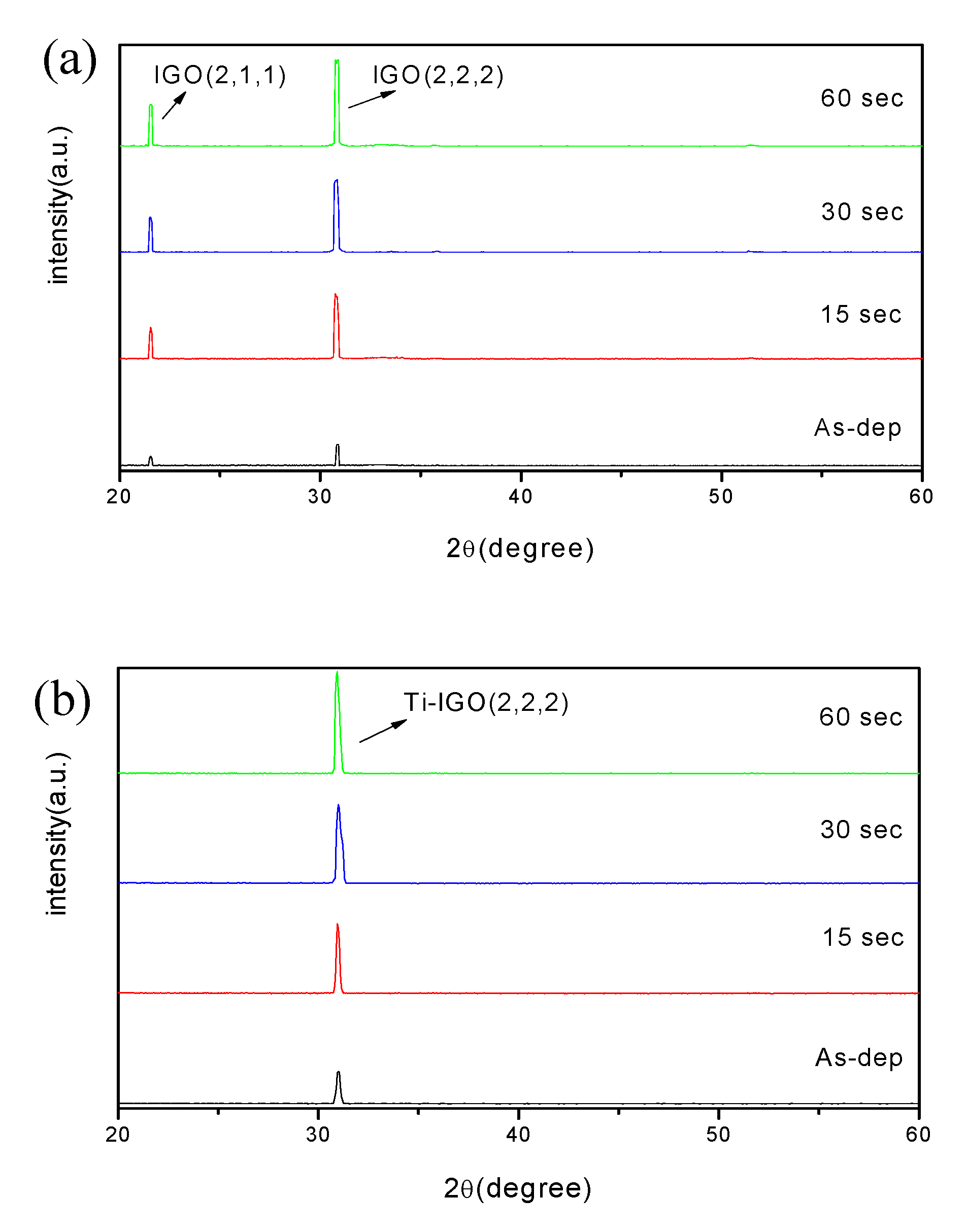
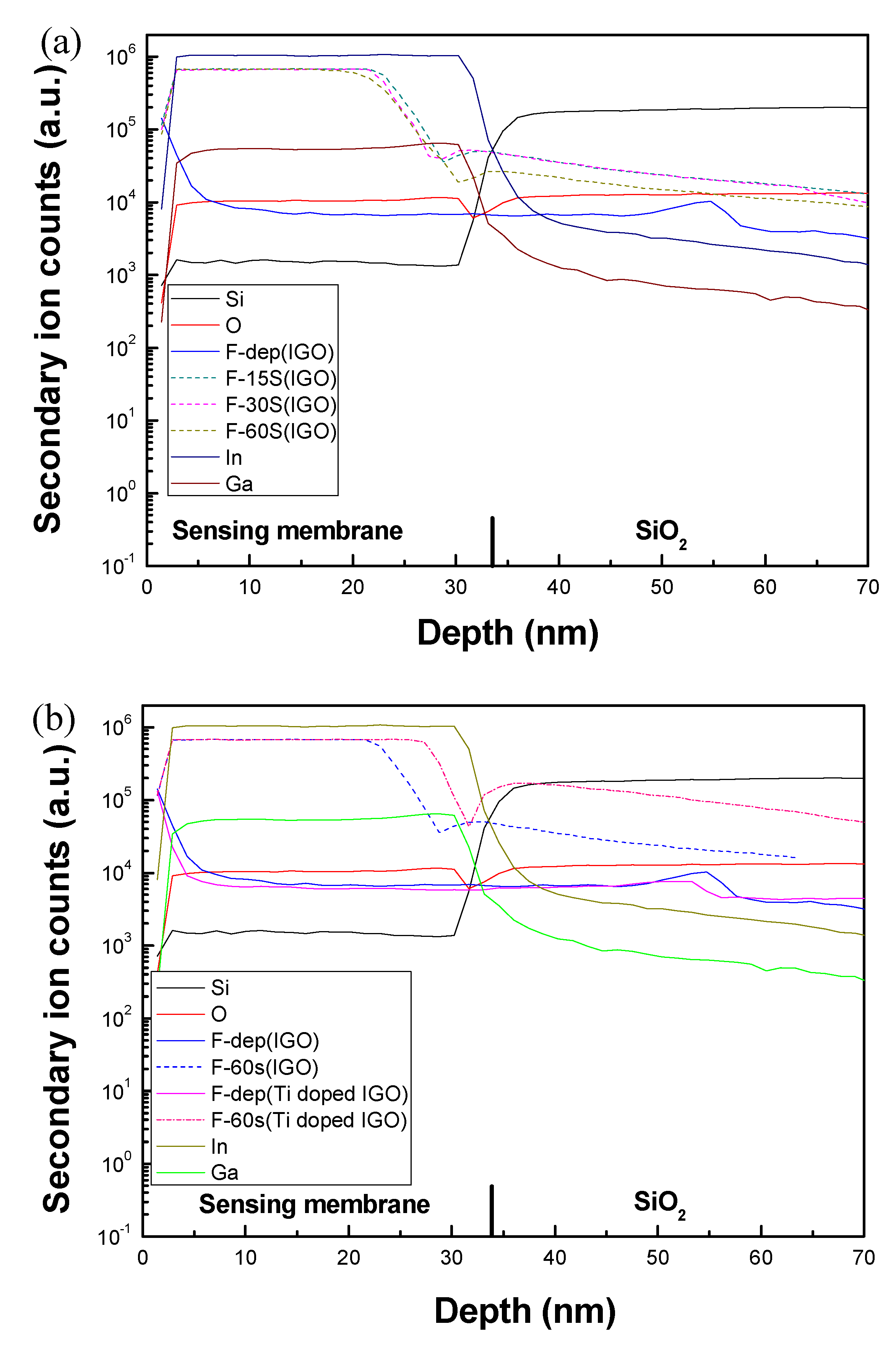
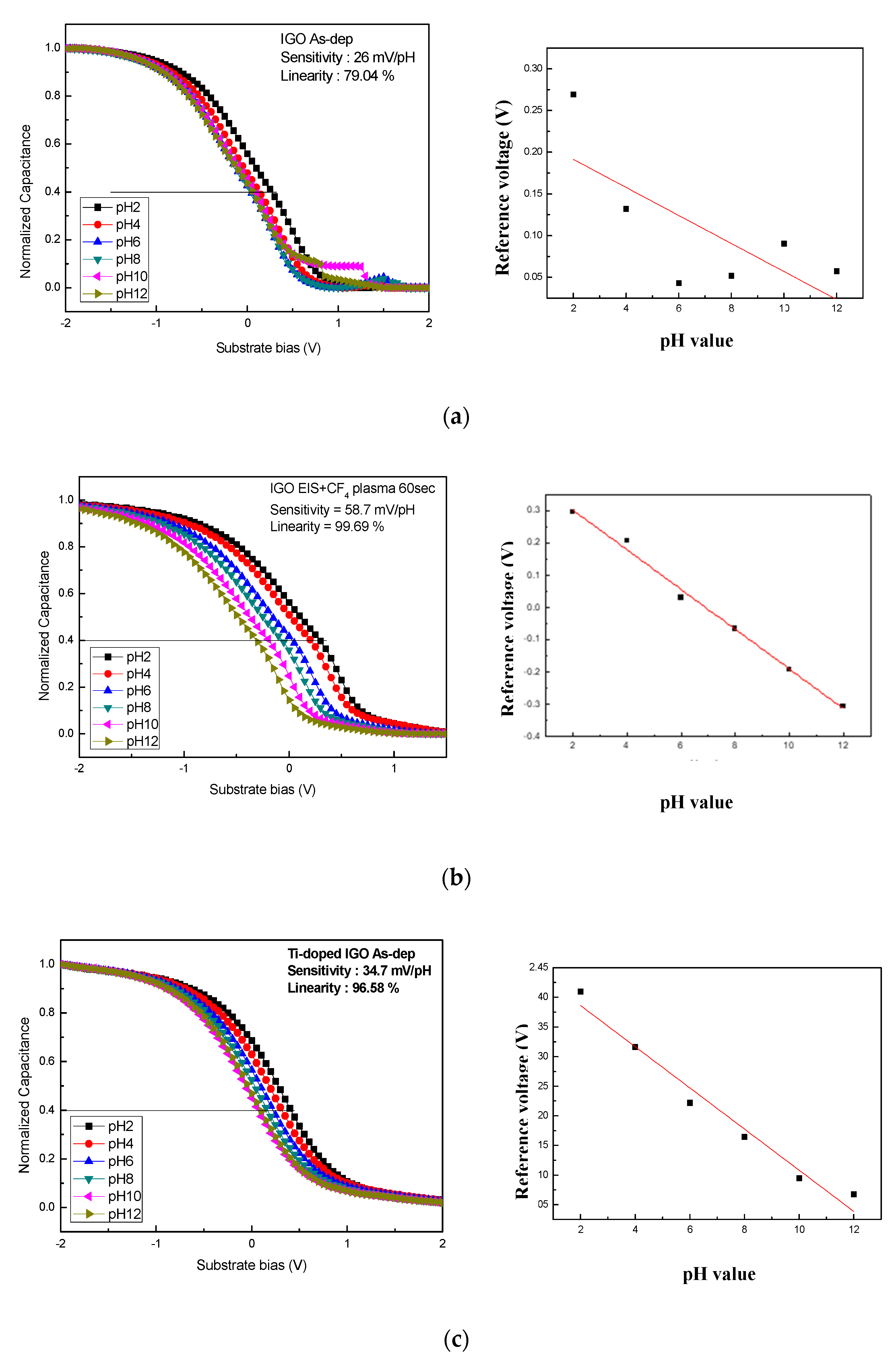
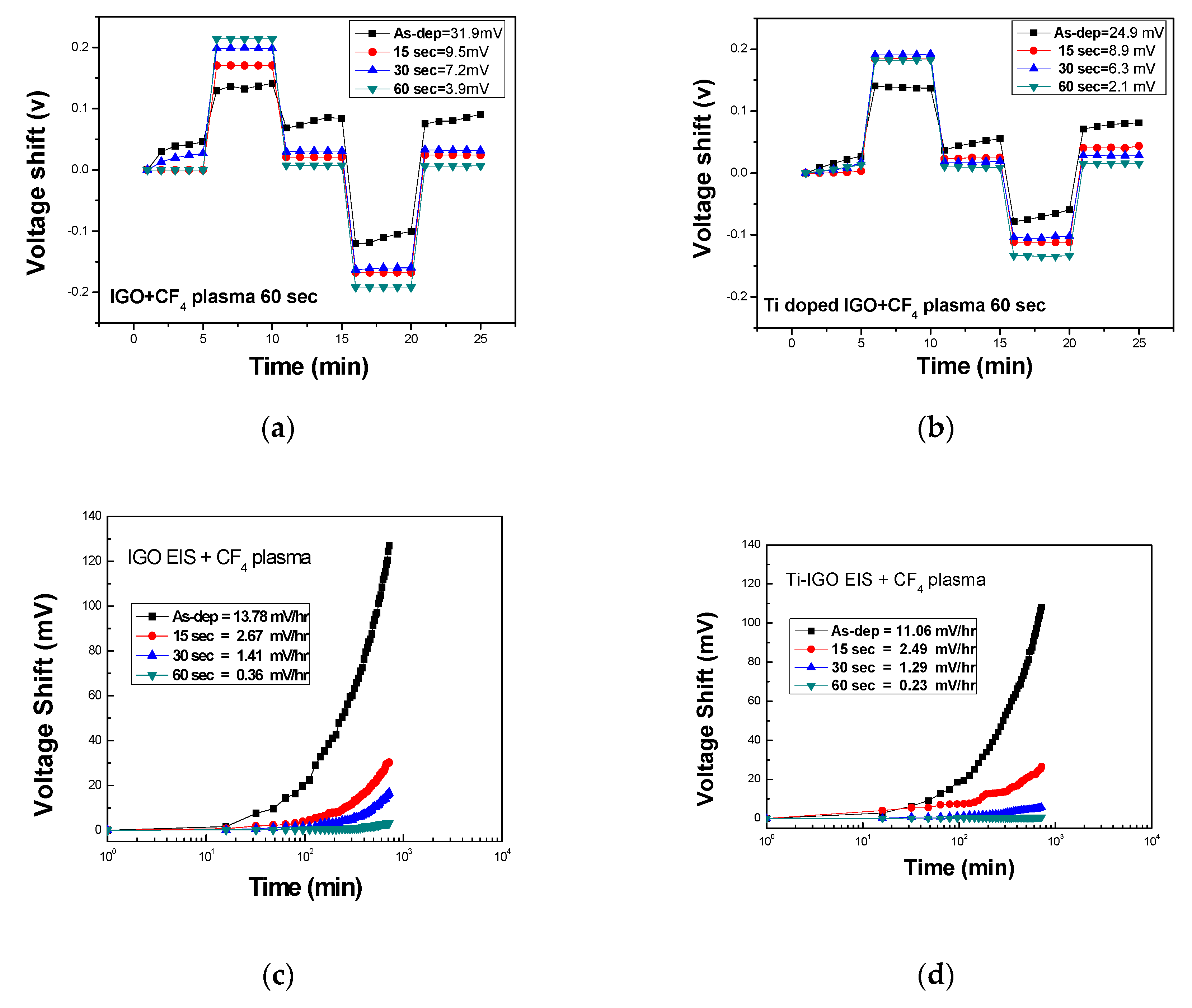
3. Results and Discussion

To study the compositional changes and the crystalline structure of IGO and Ti-doped IGO films, due to CF4 plasma treatment, the crystalline structure of the as-deposited membrane and the membrane with post-CF4 plasma treatment were monitored by using X-ray diffraction (XRD), as shown in Figure 2a,b. The XRD equipment was Bruker D8 Discover with Oxford Cryo Drive 3.0.
All the IGO samples had two diffraction peaks (211) and (222) at 21.55° and 30.85°, while Ti-doped IGO samples had only one (222) phase, indicating that Ti doping enhanced the single crystalline phase [1]. Moreover, CF4 plasma treatment enhanced (211) and (222) peaks for the IGO samples and Ti-doped IGO samples. By appropriating CF4 plasma treatment, the crystalline structures of un-doped IGO and Ti-doped IGO were enhanced. In addition, CF4 plasma treatment for 60 s had the strongest crystalline phases for both IGO and Ti-doped IGO samples.
To examine the chemical binding, the F 1s X-ray photoelectron spectroscopy (XPS) spectra of IGO and Ti-doped IGO film for the as-deposited sample and the samples treated by CF4 plasma at different conditions in 15, 30 and 60 s are shown in Figure 3a,b. The XPS equipment was Thermo scientific VG Microlab 350 Odessa, TX, USA.
The IGO film with fluorine incorporation as a gate dielectric demonstrated superior performance improvement and electrical reliability because the oxygen vacancies could be compensated, and defects could be passivated by fluorine atoms. Consequently, due to the longer CF4 plasma treatment, the sample with CF4 plasma 60 s had stronger binding energies both for Ti-doped and un-doped samples than all the other conditions [15].
Furthermore, secondary ion mass spectrometry (SIMS) was used to evaluate the diffusion of fluorine atoms caused by 60 s CF4 plasma treatment, as shown in Figure 4a,b. The SIMS equipment is ION-TOF-SIMS-V, Münster, Germany.
Notably, for the un-doped films, fluorine concentration became around 700 times near the surface, and the penetration depth was around 20 nm for the plasma treatment samples with various treatment times, as shown in Figure 4a. As for the Ti-doped sample shown in Figure 4b, the fluorine plasma treatment with 60 s can further push the penetration depth up to 25 nm. CF4 plasma with a longer treatment time of 60 s and Ti doping can activate the fluorine atoms to move further downward. The accumulation of fluorine atoms in the bulk and near the interface was demonstrated, and fluorine atoms diffused deeper for the Ti-doped sample than for the un-doped sample for some unknown reason. Moreover, the F distribution spike for the Ti-doped sample was higher than the un-doped sample. Therefore, the Ti-doped sample had better material properties and sensing performance due to better distribution of the fluorine atoms.
To characterize the surface grainization of the membranes caused by Ti doping, atomic force microscope (AFM) images were taken to measure the surface roughness of the as-deposited IGO membrane, the IGO membrane treated with 60 s CF4 plasma, the as-deposited Ti-doped IGO membrane and the Ti-doped IGO membrane treated with 60 s CF4 plasma, as shown in Figure 5a–d.
To study the trend of changes in surface roughness, the surface roughness values for the samples in various treatment were graphed as shown in Figure 5e. Notably, for both the un-doped and Ti-doped samples, the roughness increased with the increase in CF4 treatment time. Moreover, for the same CF4 plasma treatment time, the Ti-doped sample had higher roughness values than the un-doped samples. The results indicate that CF4 plasma treatment and Ti doping enhanced grainization and increased the surface roughness, which was in line with XRD analysis.
To study the pH sensing performance of all the samples, capacitance–voltage (C–V) curves were measured to evaluate the substrate voltage changes versus the variation in pH values with the capacitance value set to 0.4 Cmax. C–V curves for the as-deposited IGO sample, the IGO sample with 60 s CF4 plasma treatment, the as-deposited Ti-doped IGO sample, and the Ti-doped IGO sample with 60 s CF4 plasma treatment are shown in Figure 6a–d. Results indicate that Ti doping and CF4 plasma treatment for 60 s greatly enhanced pH sensing sensitivity and linearity consistent with all the material analyses [11,16]. Moreover, the sensitivity and linearity of all the IGO and Ti-doped samples were plotted as shown in Figure 6e,f. Ti doping and CF4 plasma treatment can incorporate Ti atoms and F atoms into the membrane, resulting in the removal of dangling bonds and traps in the bulk and near the surface. Therefore, the film quality became improved and more uniform. Therefore, compared with the as-deposited film, the distortion of C–V curves can be mitigated, which subsequently optimizes linearity. Similarly, the results indicate that CF4 plasma treatment and Ti doping improved material quality and sensing behaviors.
When compared with the previous works related to CF4 plasma treatment and IGO membranes shown in Table 1, Ti-doped IGO with plasma treatment had the highest sensitivity and linearity, indicating that Ti doping plus plasma treatment on IGO membranes can optimize the sensing performance.
To investigate the reliability problems of the IGO and Ti-doped IGO membrane, hysteresis voltages and drift voltages of the IGO and Ti-doped IGO samples were measured, as shown in Figure 7a–d. Corresponding with all the previous sensing measurements and material analyses, Ti doping and CF4 plasma treatment made the membrane more stable and reliable. To investigate the hysteresis effects, all the tested samples were immersed in buffer solutions with various pH values in a sequential cycle (pH = 7, 4, 7, 10, and 7). For each solution, the immersing time was 5 minutes. Because Ti doping and CF4 plasma treatment reduced dangling bonds and traps since Ti atoms and F atoms bound with dangling bonds and fill in traps, the sensing behavior was boosted. Therefore, the Ti-doped IGO sample with CF4 plasma treatment had the lowest hysteresis voltage.
Moreover, the drift effect of all the IGO and Ti-doped IGO membranes was measured by putting the samples in a pH 7 buffer solution for 12 h, as shown in Figure 7c,d. Similarly, the Ti-doped samples had smaller drift rates, and CF4 plasma treatment suppressed the drift voltage; thus, the Ti-doped membrane with 60 s CF4 plasma treatment had the lowest drift rate because Ti doping and F atoms incorporated from the CF4 plasma reduced the defects. Therefore, the drift voltage caused by the ion binding with the dangling bonds was drastically mitigated. The samples with CF4 plasma treatment and Ti doping had better reliability than those without doping and treatment.

4. Conclusions

In this study, Ti-doped IGO membranes were fabricated in the EIS structure. To characterize the effects of Ti doping and CF4 plasma treatment, multiple material analyses were performed. Results indicate that Ti doping and CF4 plasma treatment enhanced crystallization, grainization and chemical bindings. The pH-sensing behavior evaluation also reveals that Ti doping and CF4 plasma treatment for 60 s can drastically boost the membrane sensitivity higher than 60 mV/pH due to the removal of dangling bonds and traps. In addition, the hysteresis voltage and the drift voltage both dropped to 2.1 mV and 0.32 mV/h, respectively, indicating that the devices are more reliable and stable with the multi-treatment. The improvements came from the enhancement of crystallization, as revealed by XRD and AFM, and the fluorine atom penetration as shown by the SIMS data. Therefore, the electric field can more effectively pass through the membrane, and the capacitance and sensitivity increase. Ti-doped IGO membranes with CF4 plasma treatment are promising for future biomedical applications.

Author Contributions

Conceptualization, C.-H.K., Y.-L.S.; methodology, Y.-L.S.; software, W.-J.L., W.-L.C., S.-C.T.; validation, C.-H.K., M.-H.L., H.C.; formal analysis, C.-H.K., Y.-L.S.; investigation, C.-H.K., Y.-L.S.; resources, C.-H.K., H.C.; data curation, Y.-L.S.; writing—original draft preparation, W.-J.L., W.-L.C., S.-C.T.; writing—review and editing, M.-H.L., H.C.; visualization, M.-H.L., H.C.; supervision, H.C.; project administration, M.-H.L., H.C.; funding acquisition, H.C. All authors have read and agreed to the published version of the manuscript.

Funding

This research was funded by Ministry of Science and Technology (MOST), Taiwan; grant number 107-2221-E-260-015-MY3” and “The APC was funded by National Chi Nan University”.

Conflicts of Interest

The authors declare no conflict of interest.

References

  1. Kao, C.-H.; Liu, C.S.; Xu, C.Y.; Lin, C.F.; Chen, H. Ti-doped indium gallium oxide electrolyte–insulator–semiconductor membranes for multiple ions and solutes detectors. J. Mater. Sci. Mater. Electron. 2019, 30, 20596–20604. [Google Scholar] [CrossRef]
  2. Rongming, C.; Soo, S.C.; Hoi, W.M.; Fichtenbaum, N.; Brown, D.; McCarthy, L.; Keller, S.; Feng, W.; Speck, J.S.; Mishra, U.K. Impact of CF4 Plasma Treatment on GaN. IEEE Electron Device Lett. 2007, 28, 781–783. [Google Scholar] [CrossRef]
  3. Yang, C.; Li, X.-M.; Gilron, J.; Kong, D.-f.; Yin, Y.; Oren, Y.; Linder, C.; He, T. CF4 plasma-modified superhydrophobic PVDF membranes for direct contact membrane distillation. J. Membr. Sci. 2014, 456, 155–161. [Google Scholar] [CrossRef]
  4. Zhu, Y.W.; Moo, A.M.; Yu, T.; Xu, X.J.; Gao, X.Y.; Liu, Y.J.; Lim, C.T.; Shen, Z.X.; Ong, C.K.; Wee, A.T.S.; et al. Enhanced field emission from O2 and CF4 plasma-treated CuO nanowires. Chem. Phys. Lett. 2006, 419, 458–463. [Google Scholar] [CrossRef]
  5. Cordeiro, A.L.; Nitschke, M.; Janke, A.; Helbig, R.; D’Souza, F.; Donnelly, G.T.; Willemsen, P.R.; Werner, C. Fluorination of poly(dimethylsiloxane) surfaces by low pressure CF4 plasma–physicochemical and antifouling properties. Express Polym. Lett. 2009, 3, 70–83. [Google Scholar] [CrossRef]
  6. Sahin, H.T. RF-CF4 plasma surface modification of paper: Chemical evaluation of two sidedness with XPS/ATR-FTIR. Appl. Surf. Sci. 2007, 253, 4367–4373. [Google Scholar] [CrossRef]
  7. Sima, M.; Enculescu, I.; Sima, M.; Vasile, E.; Visan, T. EIS studies of electrodeposition process of manganese and copper doped ZnO wires. Surf. Interface Anal. 2008, 40, 561–565. [Google Scholar] [CrossRef]
  8. Valentini, L.; Puglia, D.; Armentano, I.; Kenny, J.M. Sidewall functionalization of single-walled carbon nanotubes through CF4 plasma treatment and subsequent reaction with aliphatic amines. Chem. Phys. Lett. 2005, 403, 385–389. [Google Scholar] [CrossRef]
  9. Chin, C.-H.; Lu, T.-F.; Wang, J.-C.; Yang, J.-H.; Lue, C.-E.; Yang, C.-M.; Li, S.-S.; Lai, C.-S. Effects of CF4 Plasma Treatment on pH and pNa Sensing Properties of Light-Addressable Potentiometric Sensor with a 2-nm-Thick Sensitive HfO2 Layer Grown by Atomic Layer Deposition. Jpn. J. Appl. Phys. 2011, 50. [Google Scholar] [CrossRef]
  10. Lu, T.-F.; Yang, C.-M.; Wang, J.-C.; Ho, K.-I.; Chin, C.-H.; Pijanowska, D.G.; Jaroszewicz, B.; Lai, C.-S. Characterization of K+ and Na+-Sensitive Membrane Fabricated by CF4 Plasma Treatment on Hafnium Oxide Thin Films on ISFET. J. Electrochem. Soc. 2011, 158. [Google Scholar] [CrossRef]
  11. Lin, C.F.; Kao, C.H.; Lin, C.Y.; Liu, C.S.; Liu, Y.W. Comparison Between Performances of In2O3 and In2TiO5-Based EIS Biosensors Using Post Plasma CF4 Treatment Applied in Glucose and Urea Sensing. Sci. Rep. 2019, 9, 3078. [Google Scholar] [CrossRef] [PubMed] [Green Version]
  12. Kao, C.H.; Chang, C.L.; Su, W.M.; Chen, Y.T.; Lu, C.C.; Lee, Y.S.; Hong, C.H.; Lin, C.Y.; Chen, H. Magnesium Oxide (MgO) pH-sensitive Sensing Membrane in Electrolyte-Insulator-Semiconductor Structures with CF4 Plasma Treatment. Sci. Rep. 2017, 7, 7185. [Google Scholar] [CrossRef] [PubMed] [Green Version]
  13. Kao, C.H.; Chen, H.; Hou, F.Y.S.; Chang, S.W.; Chang, C.W.; Lai, C.S.; Chen, C.P.; He, Y.Y.; Lin, S.-R.; Hsieh, K.M.; et al. Fabrication of multianalyte CeO2 nanograin electrolyte–insulator–semiconductor biosensors by using CF4 plasma treatment. Sens. Bio-Sens. Res. 2015, 5, 71–77. [Google Scholar] [CrossRef] [Green Version]
  14. Zong, X.; Zhu, R.; Guo, X. Nanostructured gold microelectrodes for SERS and EIS measurements by incorporating ZnO nanorod growth with electroplating. Sci. Rep. 2015, 5, 16454. [Google Scholar] [CrossRef] [PubMed] [Green Version]
  15. Denisenko, A.; Romanyuk, A.; Pietzka, C.; Scharpf, J.; Kohn, E. Surface structure and surface barrier characteristics of boron-doped diamond in electrolytes after CF4 plasma treatment in RF-barrel reactor. Diam. Relat. Mater. 2010, 19, 423–427. [Google Scholar] [CrossRef]
  16. Kao, C.H.; Chang, C.W.; Chen, Y.T.; Su, W.M.; Lu, C.C.; Lin, C.Y.; Chen, H. Influence of NH3 plasma and Ti doping on pH-sensitive CeO2 electrolyte-insulator-semiconductor biosensors. Sci. Rep. 2017, 7, 2405. [Google Scholar] [CrossRef] [PubMed]
  17. Huang, H.-M.; Liu, C.-H.; Lee, V.; Lee, C.; Wang, M.-J. Highly sensitive glucose biosensor based on CF4-plasma-modified interdigital transducer array (IDA) microelectrode. Sens. Actuators B Chem. 2010, 149, 59–66. [Google Scholar] [CrossRef]
  18. Park, S.H.; Kim, S.D. Plasma surface treatment of HDPE powders by CF4 plasma in a fluidized bed reactor. Polym. Bull. 1998, 41, 479–486. [Google Scholar] [CrossRef]
  19. Sahin, H.T.; Manolache, S.; Young, R.A.; Denes, F. Surface fluorination of paper in CF4-RF plasma environments. Cellulose 2002, 9, 171–181. [Google Scholar] [CrossRef]
Figure 1. Device structure of indium gallium oxide electrolyte–insulator–semiconductor (IGO EIS)-based sensors.
Crystals 10 00810 g001
Figure 2. XRD patterns of (a) the IGO films and (b) Ti-doped IGO films. (a. u. stands for arbitrary unit).
Crystals 10 00810 g002
Figure 3. The F 1s XPS spectra of (a) IGO and (b) Ti-doped IGO films with CF4 plasma. (a. u. stands for arbitrary unit).
Crystals 10 00810 g003
Figure 4. Secondary ion mass spectrometry (SIMS) profiles of (a) the IGO sensing membrane and (b) the Ti-doped IGO sensing membrane with CF4 treatment for various time. (a. u. stands for arbitrary unit).
Crystals 10 00810 g004
Figure 5. AFM images of the IGO and Ti-doped IGO surface after CF4 plasma treatment for various membranes: (a) IGO as-deposited (as-dep) film, (b) IGO with CF4 60 s (c) Ti-doped IGO as-dep, (d) Ti-doped IGO with CF4 60 s (e). The roughness versus treatment different conditions for the IGO and Ti-doped IGO membrane. The AFM equipment was Bruker Dimension Icon.
Crystals 10 00810 g005
Figure 6. Normalized capacitance–voltage (C–V) curves of the samples without and with CF4 plasma treatment at various conditions (the inset figure represents the sensitivity and linearity). (a) IGO as-dep, (b) IGO with CF4 60 s, (c) Ti-doped IGO as-dep, and (d) Ti-doped IGO with CF4 60 s. Sensitivity and linearity for (e) the IGO membrane and (f) Ti-doped IGO membrane with CF4 plasma treatment for various lengths of time.
Crystals 10 00810 g006aCrystals 10 00810 g006b
Figure 7. Hysteresis voltages of various IGO and Ti-doped IGO sensing membranes with CF4 plasma treatment in various conditions during the pH loop of 7→4→7→10→7 over a period of 25 minutes. (a) IGO and (b) Ti-doped IGO with CF4 plasma. The drift voltage of IGO and Ti-doped IGO sensing membranes treated with CF4 plasma treatment in various conditions, while being dipped in pH 7 buffer solution for 12 h. (c) IGO and (d) Ti-doped IGO with CF4 plasma.
Crystals 10 00810 g007
Table 1. Comparison of CF4 plasma treated Ti-doped IGO with previous literature.
Sensitivity (mV/pH)Linearity (%)Reference
Ti-doped IGO (CF4 plasma)60.899.87This work
Ti-doped IGO (annealing at 600 °C)59.698.2[1]
IGO (CF4 plasma)58.799.69This work
In2TiO5 (As-deposited)36.3494.23[13]
In2TiO5 (CF4 plasma)59.6499.68[13]
Nb2O5 (As-deposited)32.7693.51[5]
Nb2O5 (CF4 plasma)52.1298.22[5]

