In Situ Electric-Field Study of Surface Effects in Domain Engineered Pb(In1/2Nb1/2)O3-Pb(Mg1/3Nb2/3)O3-PbTiO3 Relaxor Crystals by Grazing Incidence Diffraction

 ,
,  , , and
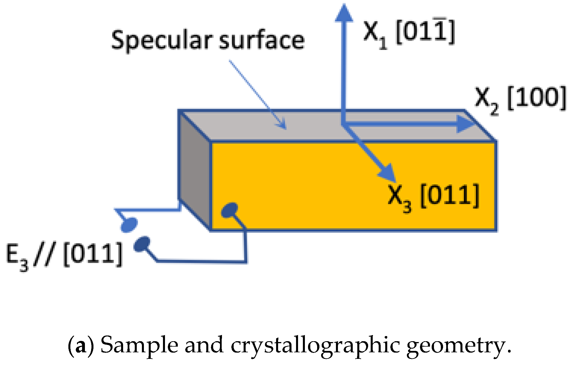
Abstract
1. Introduction
2. Results and Discussion
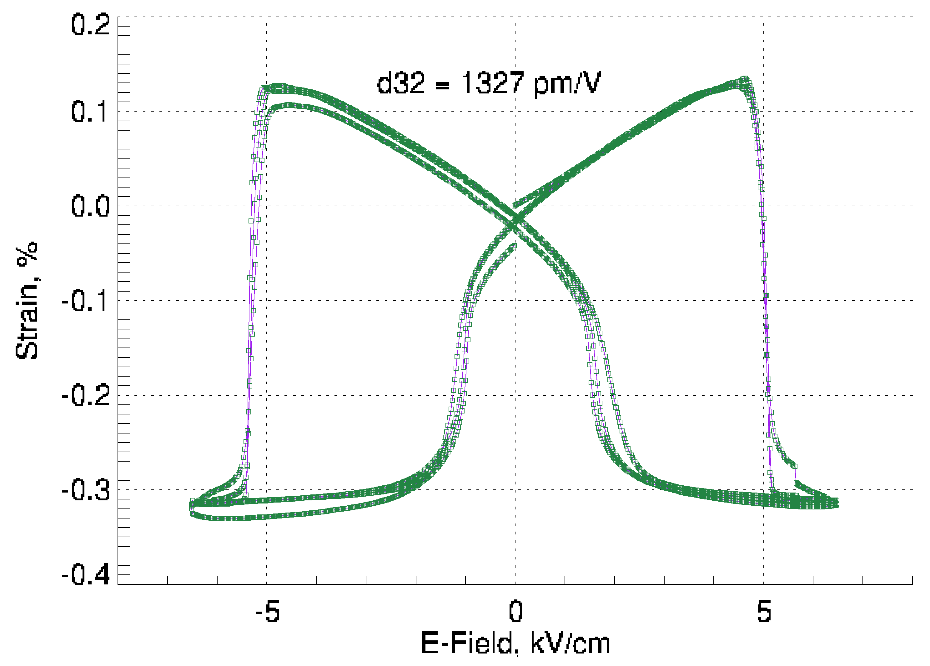
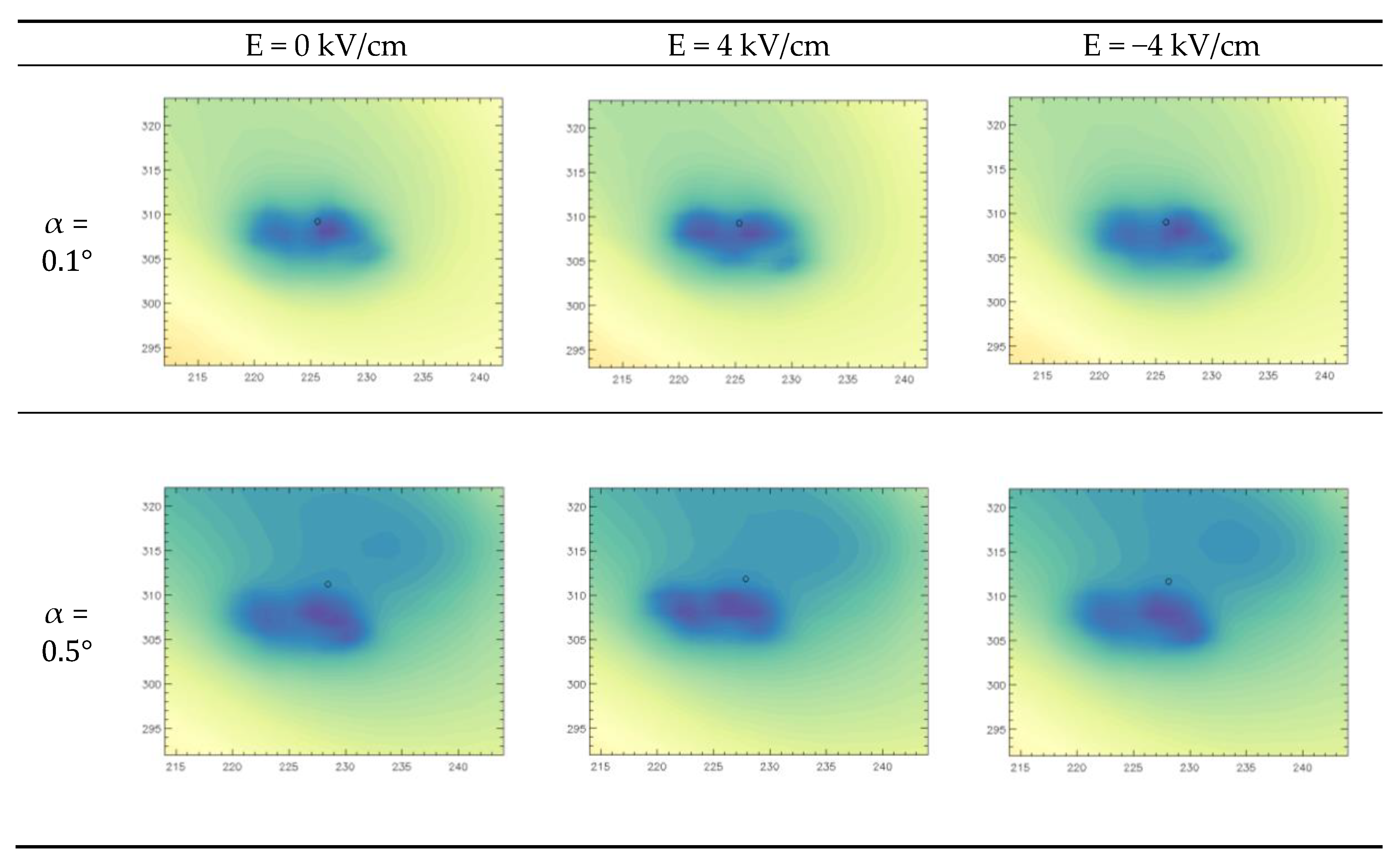
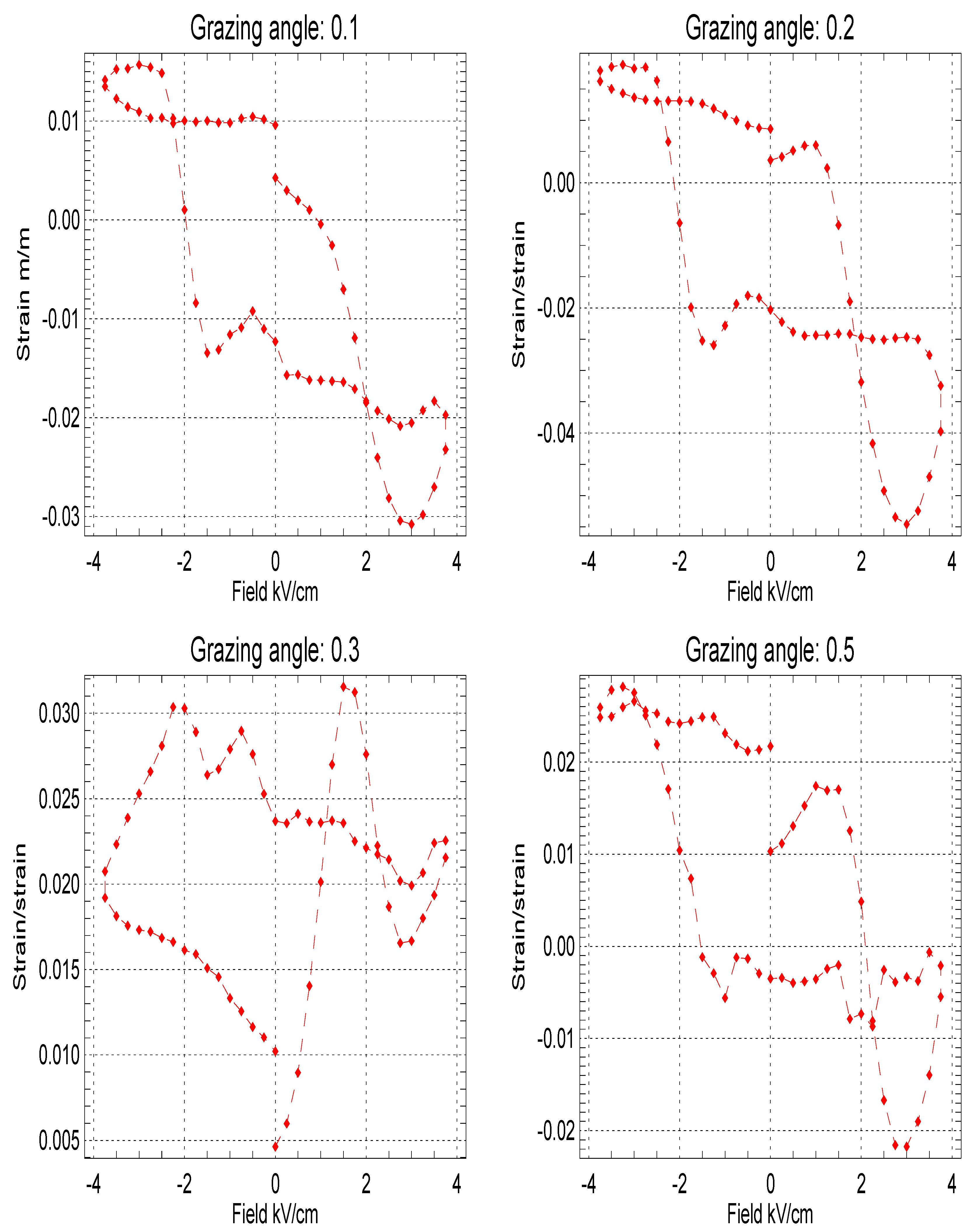
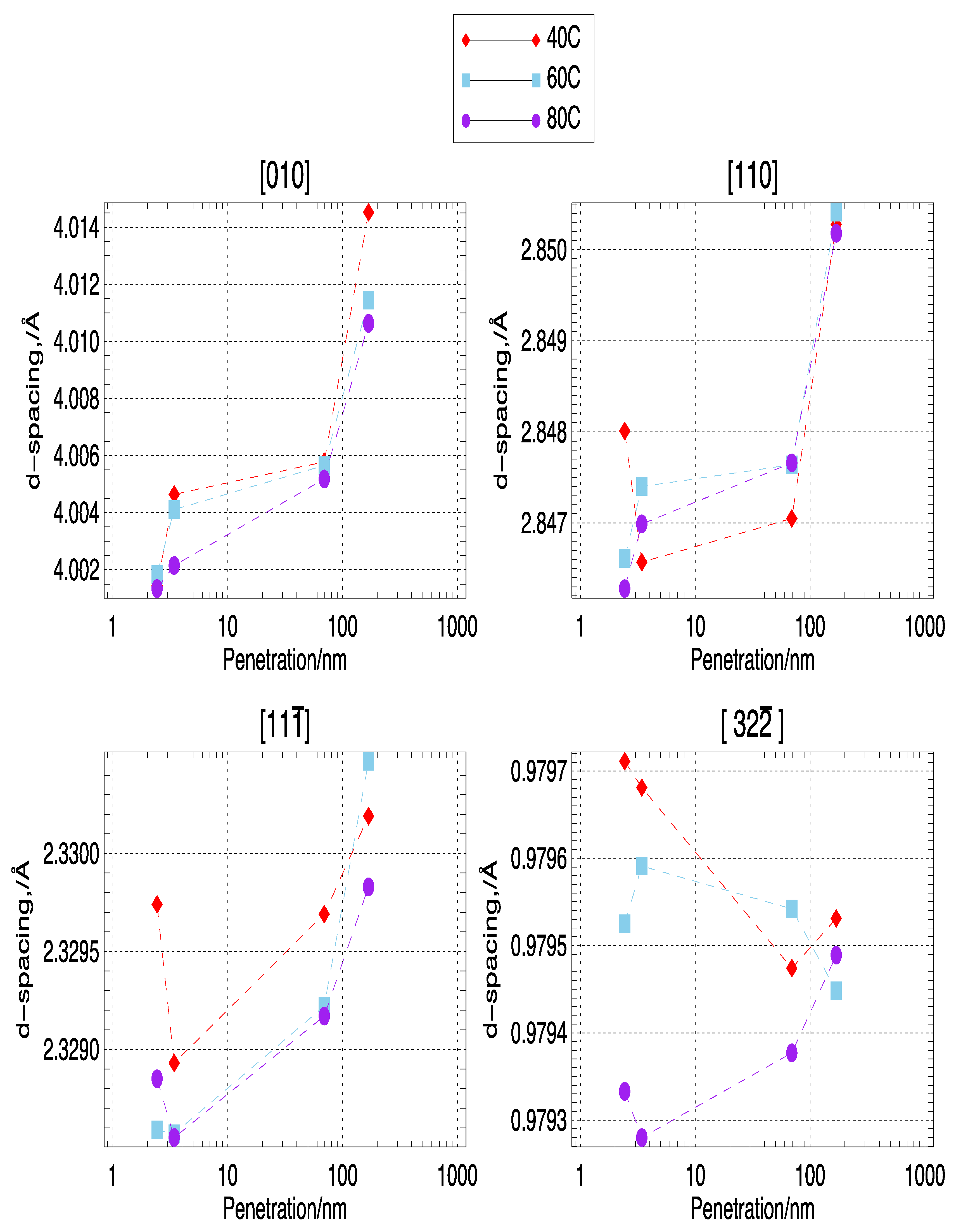
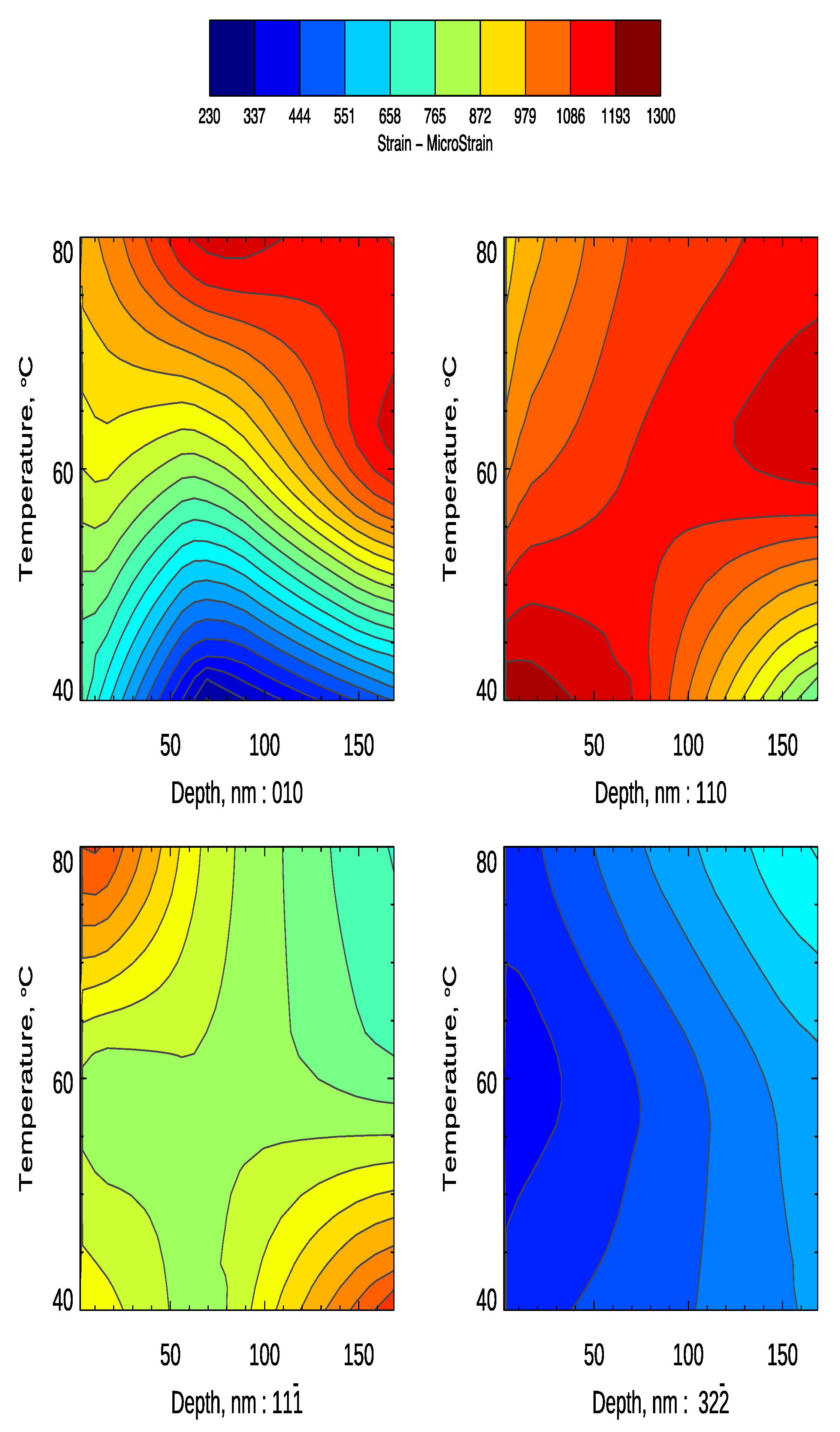
2.1. Results
2.2. Discussion
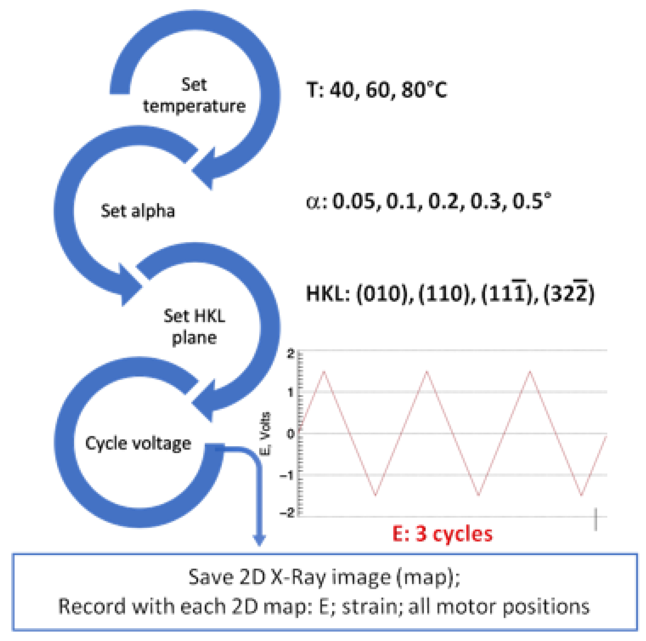
3. Experimental Section
4. Conclusions
Supplementary Materials
Author Contributions
Funding
Conflicts of Interest
References
- Park, S.E.E.; Hackenberger, W. High performance single crystal piezoelectrics: Applications and issues. Curr. Opin. Solid State Mater. Sci. 2002, 6, 11–18. [Google Scholar] [CrossRef]
- Zhang, S.; Shrout, T. Relaxor-PT single crystals: Observations and developments. IEEE Trans. Ultrason. Ferroelectr. Freq. Contr. 2010, 57, 2138–2146. [Google Scholar] [CrossRef] [PubMed]
- Sun, E.; Cao, W. Relaxor-based ferroelectric single crystals: Growth, domain engineering, characterization and applications. J. Prog. Mater. Sci. 2014, 65, 124–210. [Google Scholar] [CrossRef] [PubMed]
- Hosono, Y.; Yamashita, Y. Piezoelectric ceramics and single crystals for ultrasonic medical transducers. J. Electroceram 2006, 17, 577–583. [Google Scholar] [CrossRef]
- Li, F.; Zhang, S.; Luo, J.; Geng, X.; Xu, Z.; Shrout, T.R. [111]-oriented PIN-PMN-PT crystals with ultrahigh dielectric permittivity and high frequency constant for high-frequency transducer applications. J. Appl. Phys. 2016, 120, 074105. [Google Scholar] [CrossRef]
- Qiao, H.; He, C.; Wang, Z.; Li, X.; Liu, Y.; Tailor, H.; Long, X. Orientation-dependent electrical property and domain configuration of Mn-doped Pb(In 0.5Nb 0.5)O 3-PbTiO 3single crystal. J. Am. Ceram. Soc. 2018, 102, 79–84. [Google Scholar] [CrossRef]
- Li, F.; Zhang, S.; Xu, Z.; Wei, X.; Luo, J.; Shrout, T.R. Investigation of Electromechanical Properties and Related Temperature Characteristics in Domain-Engineered Tetragonal Pb(In1/2Nb1/2)O3-Pb(Mg1/3Nb2/3)O3-PbTiO3 Crystals. J. Am. Ceram. Soc. 2010, 93, 2731–2734. [Google Scholar] [CrossRef]
- Bell, A.J. Ferroelectrics: The role of ceramic science and engineering. J. Eur. Ceram. Soc. 2008, 28, 1307–1317. [Google Scholar] [CrossRef]
- Damjanovic, D.; Brem, F.; Setter, N. Crystal orientation dependence of the piezoelectric d[sub 33] coefficient in tetragonal BaTiO[sub 3] as a function of temperature. Appl. Phys. Lett. 2002, 80, 652. [Google Scholar] [CrossRef]
- Damjanovic, D. Contributions to the Piezoelectric Effect in Ferroelectric Single Crystals and Ceramics. J. Am. Ceram. Soc. 2005, 88, 2663–2676. [Google Scholar] [CrossRef]
- Damjanovic, D. A morphotropic phase boundary system based on polarization rotation and polarization extension. Appl. Phys. Lett. 2010, 97, 062906. [Google Scholar] [CrossRef]
- Finkel, P.; Staruch, M.; Amin, A.; Ahart, M.; Lofland, S.E. Simultaneous Stress and Field Control of Sustainable Switching of Ferroelectric Phases. Sci. Rep. 2015. [Google Scholar] [CrossRef] [PubMed]
- Nan, C.-W.; Bichurin, M.I.; Dong, S.; Viehland, D.; Srinivasan, G. Multiferroic magnetoelectric composites: Historical perspective, status, and future directions. J. Appl. Phys. 2008, 103, 031101. [Google Scholar] [CrossRef]
- Noheda, B.; Cox, D.; Shirane, G.; Gonzalo, J.; Cross, L.; Park, S. A monoclinic ferroelectric phase in the Pb (ZrTi) O solid solution. Appl. Phys. Lett. 1999, 74, 2059. [Google Scholar] [CrossRef]
- Fu, H.; Cohen, R. Polarization rotation mechanism for ultrahigh electromechanical response in single-crystal piezoelectrics. Nature 2000, 403, 281–283. [Google Scholar] [CrossRef]
- Park, S.-E.; Shrout, T.R. Ultrahigh strain and piezoelectric behavior in relaxor based ferroelectric single crystals. J. Appl. Phys. 1997, 82, 1804. [Google Scholar] [CrossRef]
- Wang, Y.; Wang, D.; Yuan, G.; Ma, H.; Xu, F.; Li, J.; Viehland, D.; Gehring, P.M. Fragile morphotropic phase boundary and phase stability in the near-surface region of the relaxor ferroelectric (1-x) Pb (Z n1 /3N b2 /3) O3-x PbTi O3: [001] field-cooled phase diagrams. Phys. Rev. B 2016, 94, 174103. [Google Scholar] [CrossRef]
- Xu, G.; Gehring, P.M.; Stock, C.; Conlon, K. The anomalous skin effect in single crystal relaxor ferroelectric PZN-x PT and PMN-x PT. Phase Transit. 2006, 79, 135–152. [Google Scholar] [CrossRef]
- Cowley, R.A.; Gvasaliya, S.N.; Lushnikov, S.G.; Roessli, B.; Rotaru, G.M. Relaxing with relaxors: A review of relaxor ferroelectrics. Adv. Phys. 2011, 60, 229–327. [Google Scholar]
- Phelan, D.; Rodriguez, E.E.; Gao, J.; Bing, Y.; Ye, Z.G.; Huang, Q.; Wen, J.; Xu, G.; Stock, C.; Matsuura, M.; et al. Phase diagram of the relaxor ferroelectric (1-x) Pb(Mg1/3Nb2/3)O3+xPbTiO3 revisited: A neutron powder diffraction study of the relaxor skin effect. Phase Transit. 2015, 88, 283–305. [Google Scholar] [CrossRef]
- Xu, G.; Zhong, Z.; Bing, Y.; Ye, Z.G.; Stock, C.; Shirane, G. Ground state of the relaxor ferroelectric Pb(Zn1/3Nb2/3)O3. Phys. Rev. B Condens. Matter 2003, 67, 1804–1805. [Google Scholar] [CrossRef]
- Wang, Y.; Yuan, G.; Luo, H.; Li, J.; Viehland, D. Phase Transition in the Near-Surface Region of Ternary Pb(In1/2Nb1/2)O3−Pb(Mg1/3Nb2/3)O3−PbTiO3Relaxor Ferroelectric Crystals. Phys. Rev. Appl. 2017, 8, 034032. [Google Scholar] [CrossRef]
- Feidenhans’l, R. Surface structure determination by X-ray diffraction. Surf. Sci. Rep. 1989, 10, 105–188. [Google Scholar] [CrossRef]
- Lee, H.J.; Zhang, S.; Luo, J.; Li, F.; Shrout, T.R. Thickness-Dependent Properties of Relaxor-PbTiO3 Ferroelectrics for Ultrasonic Transducers. Adv. Funct. Mater. 2010, 20, 3154–3162. [Google Scholar] [CrossRef] [PubMed]
- Wang, H.; Zeng, K. Domain structure, local surface potential distribution and relaxation of Pb(Zn1/3Nb2/3)O3-9%PbTiO3 (PZN-9%PT) single crystals. J. Mater. 2016, 2, 309–315. [Google Scholar] [CrossRef]
- Qi, X.; Zhao, Y.; Sun, E.; Du, J.; Li, K.; Sun, Y.; Yang, B.; Zhang, R.; Cao, W. Large electrostrictive effect and high energy storage performance of Pr3+-doped PIN-PMN-PT multifunctional ceramics in the ergodic relaxor phase. J. Eur. Ceram. Soc. 2019, 39, 4060–4069. [Google Scholar] [CrossRef]
- Vlasov, E.O.; Chezganov, D.S.; Gimadeeva, L.V.; Ushakov, A.D.; Hu, Q.; Wei, X.; Shur, V.Y. Domain structure imaging in PMN-PT crystals using channelling-contrast backscattered electron microscopy. IOP Conf. Ser. Mater. Sci. Eng. 2018, 443, 012038. [Google Scholar] [CrossRef]
- Herdier, R.; Leclerc, G.; Poullain, G.; Bouregba, R.; Remiens, E.D.; Dogheche, E. Investigation of Piezoelectric and Electrostrictive Properties of (Pb 1-3 y/2,La y) (Zr x,Ti 1-x)O 3Ferroelectric Thin Films Using a Doppler Laser Vibrometer. Ferroelectrics 2010, 362, 145–151. [Google Scholar] [CrossRef]
- He, W.; Li, Q.; Xi, X.; Yan, Q. High temperature-insensitive ferro-/piezoelectric properties and nanodomain structures of Pb(In 1/2Nb 1/2)O 3-PbZrO 3-Pb(Mg 1/3Nb 2/3)O 3-PbTiO 3relaxor single crystals. J. Am. Ceram. Soc. 2017, 101, 1236–1244. [Google Scholar] [CrossRef]
- Detalle, M.; Herdier, R.; Wang, G.S.; Remiens, D.; Roussel, P.; Fribourg-Blanc, E. Electrostrictive and Piezoelectric Behavior of PMN-PT Thin Films. Ferroelectrics 2007, 351, 15–24. [Google Scholar] [CrossRef]
- Patterson, E.A.; Staruch, M.; Matis, B.R.; Young, S.; Lofland, S.E.; Antonelli, L.; Blackmon, F.; Damjanovic, D.; Cain, M.G.; Thompson, P.B.J.; et al. Dynamic piezoelectric response of relaxor single crystal under electrically driven inter-ferroelectric phase transformations. Appl. Phys. Lett. 2020, 116, 222903. [Google Scholar] [CrossRef]
- Cain, M.G. Springer series in measurement science and technology. In Characterisation of Ferroelectric Bulk Materials and Thin Films; Springer: Berlin, Germany, 2014. [Google Scholar]
- Vecchini, C.; Thompson, P.; Stewart, M.; Muniz-Piniella, A.; McMitchell, S.R.C.; Wooldridge, J.; Lepadatu, S.; Bouchenoire, L.; Brown, S.; Wermeille, D.; et al. Simultaneous dynamic electrical and structural measurements of functional materials. Rev. Sci. Instrum. 2015, 86, 103901. [Google Scholar] [CrossRef] [PubMed]
- Solé, V.A.; Papillon, E.; Cotte, M.; Walter, P.; Susini, J. A multiplatform code for the analysis of energy-dispersive X-ray fluorescence spectra. Spectrochim. Acta Part. B At. Spectrosc. 2007, 62, 63–68. [Google Scholar] [CrossRef]


© 2020 by the authors. Licensee MDPI, Basel, Switzerland. This article is an open access article distributed under the terms and conditions of the Creative Commons Attribution (CC BY) license (http://creativecommons.org/licenses/by/4.0/).
Share and Cite
Cain, M.G.; Staruch, M.; Thompson, P.; Lucas, C.; Wermeille, D.; Kayser, Y.; Beckhoff, B.; Lofland, S.E.; Finkel, P. In Situ Electric-Field Study of Surface Effects in Domain Engineered Pb(In1/2Nb1/2)O3-Pb(Mg1/3Nb2/3)O3-PbTiO3 Relaxor Crystals by Grazing Incidence Diffraction. Crystals 2020, 10, 728. https://doi.org/10.3390/cryst10090728
Cain MG, Staruch M, Thompson P, Lucas C, Wermeille D, Kayser Y, Beckhoff B, Lofland SE, Finkel P. In Situ Electric-Field Study of Surface Effects in Domain Engineered Pb(In1/2Nb1/2)O3-Pb(Mg1/3Nb2/3)O3-PbTiO3 Relaxor Crystals by Grazing Incidence Diffraction. Crystals. 2020; 10(9):728. https://doi.org/10.3390/cryst10090728
Chicago/Turabian StyleCain, Markys G., Margo Staruch, Paul Thompson, Christopher Lucas, Didier Wermeille, Yves Kayser, Burkhard Beckhoff, Sam E. Lofland, and Peter Finkel. 2020. "In Situ Electric-Field Study of Surface Effects in Domain Engineered Pb(In1/2Nb1/2)O3-Pb(Mg1/3Nb2/3)O3-PbTiO3 Relaxor Crystals by Grazing Incidence Diffraction" Crystals 10, no. 9: 728. https://doi.org/10.3390/cryst10090728
APA StyleCain, M. G., Staruch, M., Thompson, P., Lucas, C., Wermeille, D., Kayser, Y., Beckhoff, B., Lofland, S. E., & Finkel, P. (2020). In Situ Electric-Field Study of Surface Effects in Domain Engineered Pb(In1/2Nb1/2)O3-Pb(Mg1/3Nb2/3)O3-PbTiO3 Relaxor Crystals by Grazing Incidence Diffraction. Crystals, 10(9), 728. https://doi.org/10.3390/cryst10090728