1. Introduction
Organic thin-film transistors (OTFTs) have attracted considerable attention in emerging electronics, such as flexible electronics and wearable electronics, due to their features of intrinsic bendability and low-cost printability [
1,
2]. In the past decades, OTFTs have been applied to various applications, including biosensors [
3,
4,
5], wearable amplifiers [
6,
7], and flexible optoelectronic systems [
8,
9,
10]. However, printed OTFTs typically demonstrate a modest performance, such as with low device mobilities and large operating voltages, which had been bottlenecks for the development of printed OTFTs [
11,
12,
13]. Recently, a report of all-inkjet printed OTFTs showing a steep subthreshold slope to the thermionic limit has opened up new possibilities of printed electronics for real-world applications [
6].
Among various semiconductor applications, optoelectronics is one of the most important branches. There have been plentiful reports on OTFTs used as photodetectors and phototransistors [
8], but only sporadic demonstrations by all-printed OTFTs [
14,
15]. In addition, most of the reports were focused on the response to ultraviolet (UV) lights [
8,
15,
16]. Therefore, it would be interesting to investigate the photo-sensitivity of all-inkjet printed OTFTs, in particular under the visible light exposure that has not been deeply investigated. Furthermore, it is also essential for the real-world applications of photodetectors, printable counterparts that are insensitive to lights to be integrated into a photodetector circuit building block or a system for signal conditioning and processing. Despite examples of using a photo-blocking layer that adds fabrication complexity and cost [
17], it is also essential to find some intrinsic methods. Typical organic semiconductors have bandgaps of around 2 eV [
6], of which the energy corresponds to a visible light, so they can be used for photo-sensitive OTFTs. To develop photo-insensitive OTFTs, wide-bandgap organic semiconductors (e.g., >3 eV) need to be used. Therefore, to develop all-inkjet printed OTFTs with and without photo-sensitivity to visible light, it is essential to use semiconductors with different bandgaps. However, it still needs to be further explored and validated whether there is a compatible fabrication method for both types of devices without adding fabrication cost and complexity.
In this study, the photoresponse of all-inkjet printed OTFTs to visible lights is investigated. Rather than developing photo-sensitive OTFTs only, an important research question is whether there is a simple OTFT fabrication process used by only a printing technique that can reliably produce both types of OTFTs with and without photo-sensitivity to visible light. To this end, two different organic semiconductors with different bandgaps are designed in the same device structure. The electrical and photo-sensing characteristics of all-inkjet printed OTFTs are measured, and their sensitivity and insensitivity to visible light are investigated.
2. Materials and Methods
2.1. Materials and Ink Formulations
Poly(1,1,2,4,4,5,5,6,7,7-decafluoro-3-oxa-1,6-heptadiene), known as CYTOP (CTL-809M), and its solvent (CT-Solv. 180) were purchased from Asahi Glass, Tokyo, Japan. 2,7-Dioctyl[1]benzothieno[3,2-b][1]benzothiophene (C8-BTBT), 6,13-bis (triisopropylsilylethynyl) pentacene (TIPS-pentacene), polystyrene (PS), polyvinyl cinnamate (PVC), and perfluorobenzenethiol (PFBT) were purchased from Sigma-Aldrich, Gillingham, UK.
The conductive silver (Ag) ink (jet-600C) was supplied by Hisense Electronics, Kunshan, China. The gate dielectric ink was prepared by dissolving PVC in anisole at a concentration of 45 mg/mL. The semiconductor inks were formulated by dissolving C8-BTBT (or TIPS-pentacene) and PS in anisole at a concentration of 10 mg/mL and then mixing the two solutions at a volume-to-volume ratio of 3:1. The addition of PS was to improve the quality of printed semiconductor thin films. For the encapsulation ink, CYTOP was diluted with its solvent at a weight-to-weight ratio of 3:1.
2.2. Device Fabrication
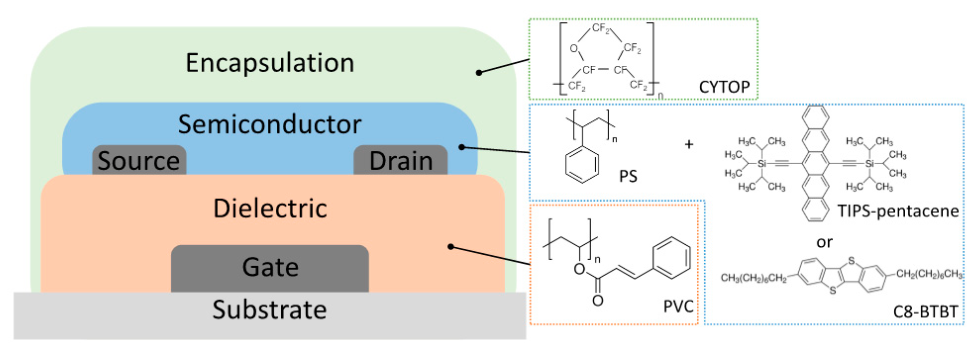
A bottom-gate bottom-contact device structure was used in this study, as shown in
Figure 1. A material inkjet printer, DMP-2831(purchased from FUJIFILM Dimatix, Lebanon, New Hampshire, USA), was used for all the fabrication processes, which were conducted in ambient air. All the inks were filled into DMPLCP-11610 cartridges (FUJIFILM Dimatix), of which the nozzles typically jet droplets at the size of around 10 pL. The waveform setting for nozzles was the same as the reported setting in the previous studies [
6,
18,
19,
20].
The Ag ink was printed on a flexible plastic polyethylene naphthalate (PEN) (Teonex®, DuPont, Wilmington, DE, USA) substrate at a drop spacing of 50 μm, followed by annealing at 130 °C for 15 min to form gate electrodes. A single nozzle was used to better control the geometrical precision of printed conductive thin films. Then, the PVC ink was printed at a drop spacing of 10 μm, and 6 consecutive nozzles were used for jetting at the same time with a cartridge angle of 11.4° (which corresponds to the setting for the drop spacing of 50 μm). Therefore, the actual PVC thin films were printed at a horizontal drop spacing of 10 μm and a vertical drop spacing of 50 μm. The printed PVC film was prebaked at 100 °C for 1 min, exposed to 254 nm UV light for 30 min, and hard-baked at 100 °C for 30 min. The thickness of the printed PVC film was measured to be around 151 nm (of which the unit-area gate capacitance was measured to be 19.9 nF/cm2). After the formation of the cross-linked PVC gate insulator, the Ag ink was printed again and then annealed at 120 °C for 15 min to form source/drain electrodes of around 100 nm, defining the channel width and length of 1200 µm and 80 µm, respectively. The source/drain electrodes were treated by a 0.1% PFBT-ethanol solution for 3 min and rinsed with ethanol. The semiconductor was printed with 3 consecutive nozzles at a drop spacing of 5 μm and annealed at 60 °C for 30 min. Finally, CYTOP ink was printed to encapsulate the devices and annealed at 60 °C for 30 min.
2.3. Material and Device Characterization
Ultraviolet–visible (UV–vis) spectroscopy measurements of TIPS-pentacene/PS and C8-BTBT/PS films on quartz substrates were made using a UniCam UV-vis spectrometer. The electrical properties of the devices were characterized with a Keithley 4200 Semiconductor Characterization System (Solon, OH, USA). The photoresponse of the devices was measured under LEDs with optical filters centering at wavelengths of 400 nm, 500 nm, 600 nm, 700 nm, and 800 nm. The light intensity for each wavelength was adjusted to 10 mW/cm2, calibrated by a Thorlabs photodetector DET10A. The LEDs, optical filters, and photodetector were from Thorlabs, Newton, NJ, USA. The illumination area was a circle with a diameter of around 5 mm. The whole area of the channel was irradiated, with the light applied from the top through the CYTOP layer.
2.4. Device Parameters Extraction
The mobility (
µ) and threshold voltage (
VT) were calculated by fitting the square root of the drain current (
ID) versus the gate voltage (
VGS) using the following equation:
where
W is the channel width,
L the channel length, and
Ci the gate dielectric capacitance per unit area. The subthreshold slope was extracted by fitting the
ID versus
VGS in the subthreshold regime using the following equation:
where
Iref is the reference current in the subthreshold regime at the reference voltage
Vref.
3. Results and Discussion
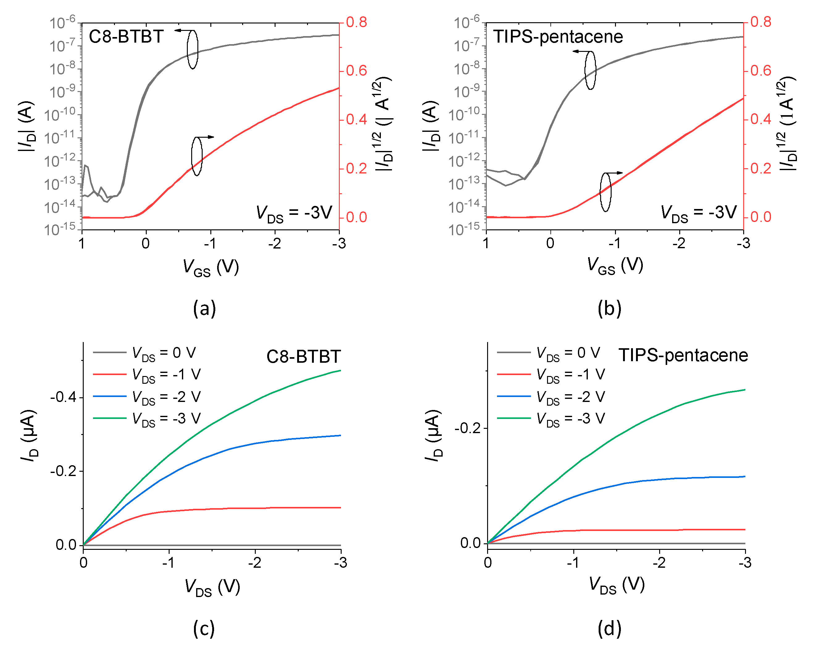
The electrical transfer and output characteristics of all-inkjet printed C8-BTBT and TIPS-pentacene OTFTs are depicted in
Figure 2. Both the devices demonstrated low operating voltages of <3 V and steep subthreshold slopes of <0.2 V/decade compared to typical printed OTFTs, due to the reduced trap density as reported in the previous studies [
6,
21]. In comparison, the C8-BTBT devices demonstrated better performance than TIPS-pentacene ones. As shown in
Figure 2a, a typical fabricated C8-BTBT OTFT exhibited a field-effect mobility of 0.42 cm
2 V
−1 s
−1, a close-to-zero
VT of 0.11 V, a high on-off ratio of >10
7, and a steep subthreshold slope of 64.8 mV/decade. Such a steep subthreshold slope value was close to the thermionic limit of 59.6 mV/decade at room temperature of 300 K. A typical TIPS-pentacene OTFT demonstrated a field-effect mobility of 0.21 cm
2 V
−1 s
−1, a small
VT of −0.21 V, a large on-off ratio of >10
6, and a steep subthreshold slope of 142.8 mV/decade. The higher on-off ratio of the C8-BTBT devices was attributed to the reported wideband gap of C8-BTBT [
6], so that the off-state current could be lower than the TIPS-pentacene devices. Both the C8-BTBT and TIPS-pentacene OTFTs exhibited negligible hysteresis, as shown in
Figure 2a,b.
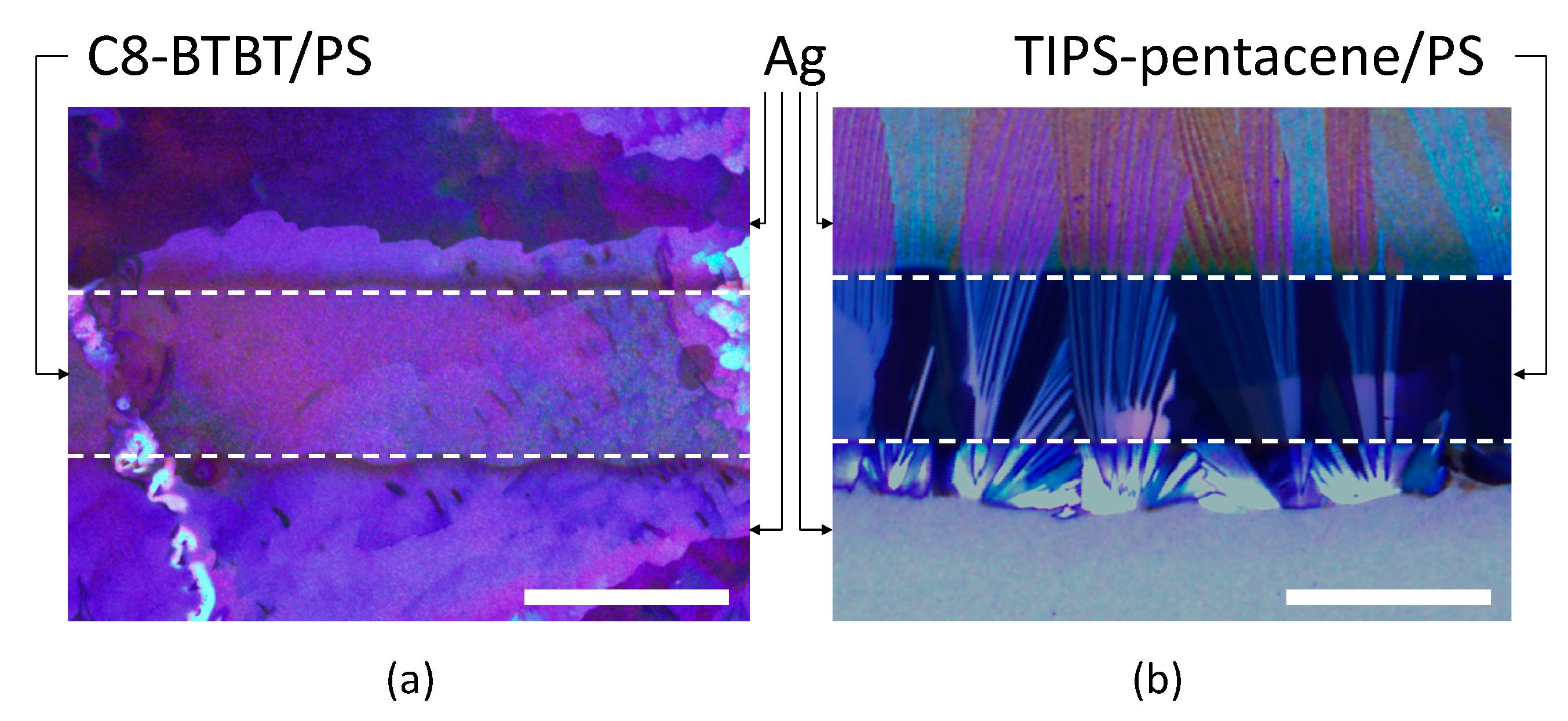
The most noticeable difference of the device parameter was the steeper subthreshold slope exhibited by the C8-BTBT OTFTs, which can be attributed to the lowered defect density in the C8-BTBT devices. As shown in
Figure 3, the printed C8-BTBT thin films formed large flake-like crystals that covered the device channel, whereas the printed TIPS-pentacene thin films had narrow needle-like crystals that consisted of considerable traps at the grain boundaries, which is in line with other reports [
21,
22]. Despite the overall better performance of C8-BTBT OTFTs, they possessed a large contact resistance when operating in the above-threshold regime (as seen from the non-linearity in the |
ID|
1/2-
VGS plot in
Figure 2a, as a result of the presence of a Schottky barrier at the semiconductor-metal contacts. The Schottky barrier was used to achieve a large channel-independent output resistance, which is promising for printed analogue electronics; however, it reduced the charge carrier injection at high current levels in the above-threshold operation, thus limiting its application to displays as active driving transistors. Therefore, for different applications, OTFTs with different materials systems should be designed and selected to maximize their performance.
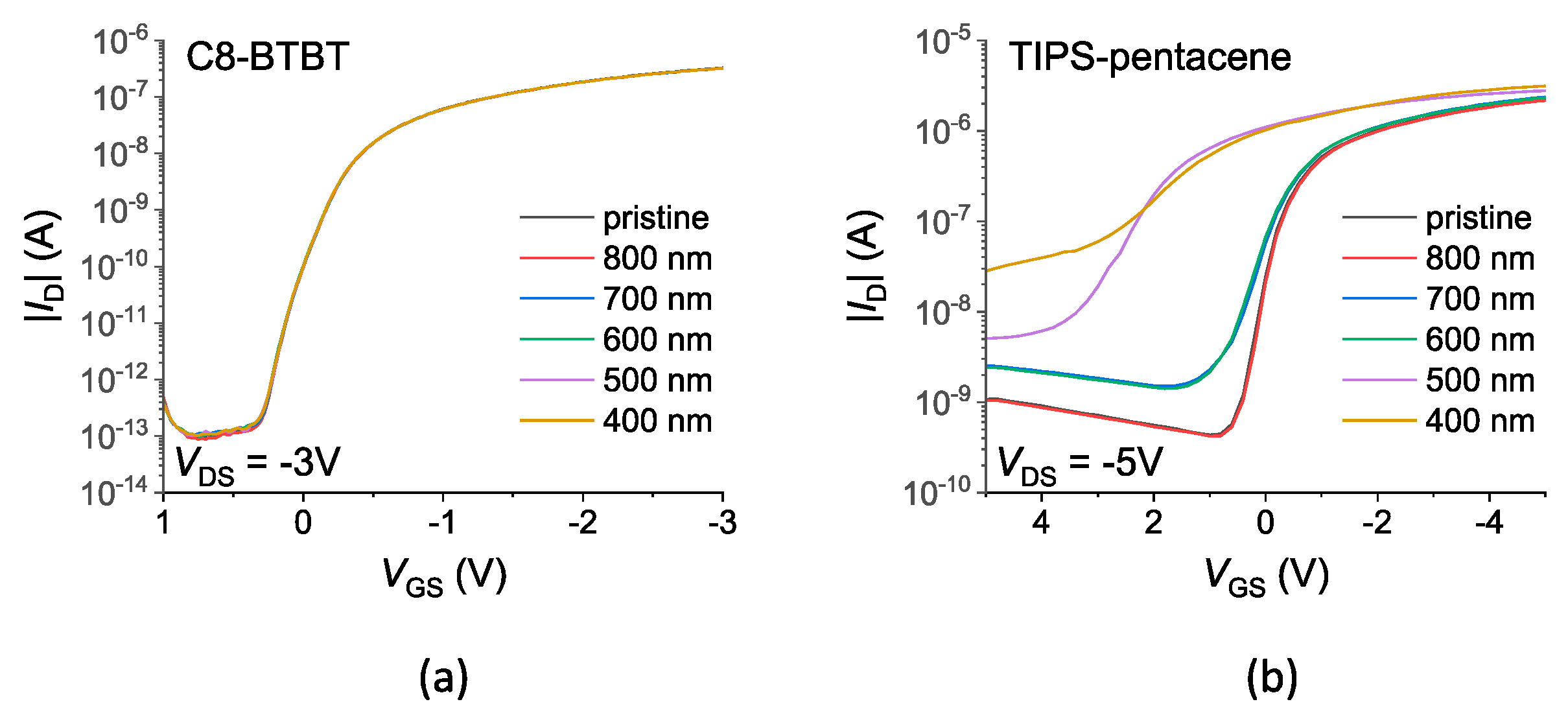
Although the devices with C8-BTBT and TIPS-pentacene as semiconductors showed minor differences of device performance under dark condition, they behaved notably differently under exposure to visible lights. The C8-BTBT OTFTs demonstrated negligible transfer characteristics changes under light exposure (400–800 nm), as seen in
Figure 4a. In contrast, although TIPS-pentacene OTFTs did not have a response to 800 nm infrared light, they responded actively to visible lights (400–700 nm), as shown in
Figure 4b. The negligible response to 800 nm infrared light suggested that the photon energy might be not large enough, given the relation between photon energy (
E) and wavelength (
λ) as
E =
hc/λ, where
h is the Planck constant,
c is the speed of light in vacuum [
23]. The TIPS-pentacene OTFTs started to show photoresponse when the wavelength of exposing light was 700 nm or below, indicating a bandgap of around 1.77 eV.
Photoresponse generally includes two mechanisms: photocurrent and threshold voltage shift [
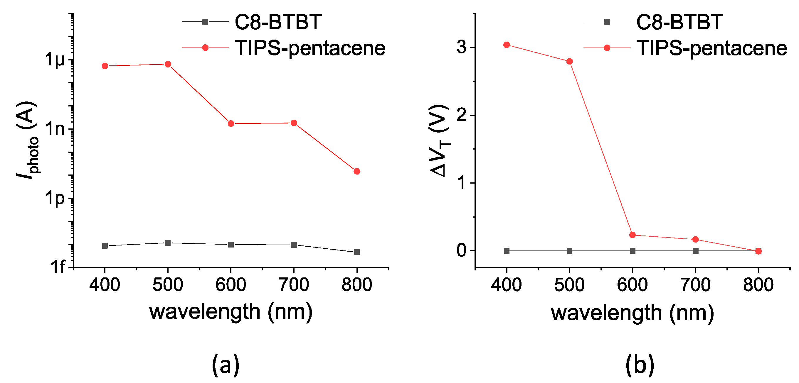
24]. When a semiconductor is exposed to lights (whose photon energy is higher than the bandgap of the semiconductor), excitons are induced. As a result, more free charge carriers are available, which under an electrical field can contribute to a photocurrent. In addition, the excess minority carriers can induce a threshold voltage shift. In this work, the excess charge carriers were electrons, thereby shifting threshold voltage positively. To characterize these effects, photocurrents and threshold voltage shifts were extracted. As shown in
Figure 5a, the C8-BTBT OTFTs demonstrated negligible photocurrents under exposure; for TIPS-pentacene, devices demonstrated noticeable photocurrents starting from 700 nm light exposure, and there was a relatively large photocurrent increase from 500 nm to 400 nm light exposure. As for the threshold voltage shifts, the C8-BTBT OTFTs seemed to be free from this effect, as shown in
Figure 5b. The TIPS-pentacene demonstrated a gradual increase in threshold voltage shifts with exposure from 800 nm light to 600 nm light and a more significant increase between 600 nm and 500 nm light exposure. The photocurrents were extracted at the
VGS of 1 V for both C8-BTBT and TIPS-pentacene OTFTs.
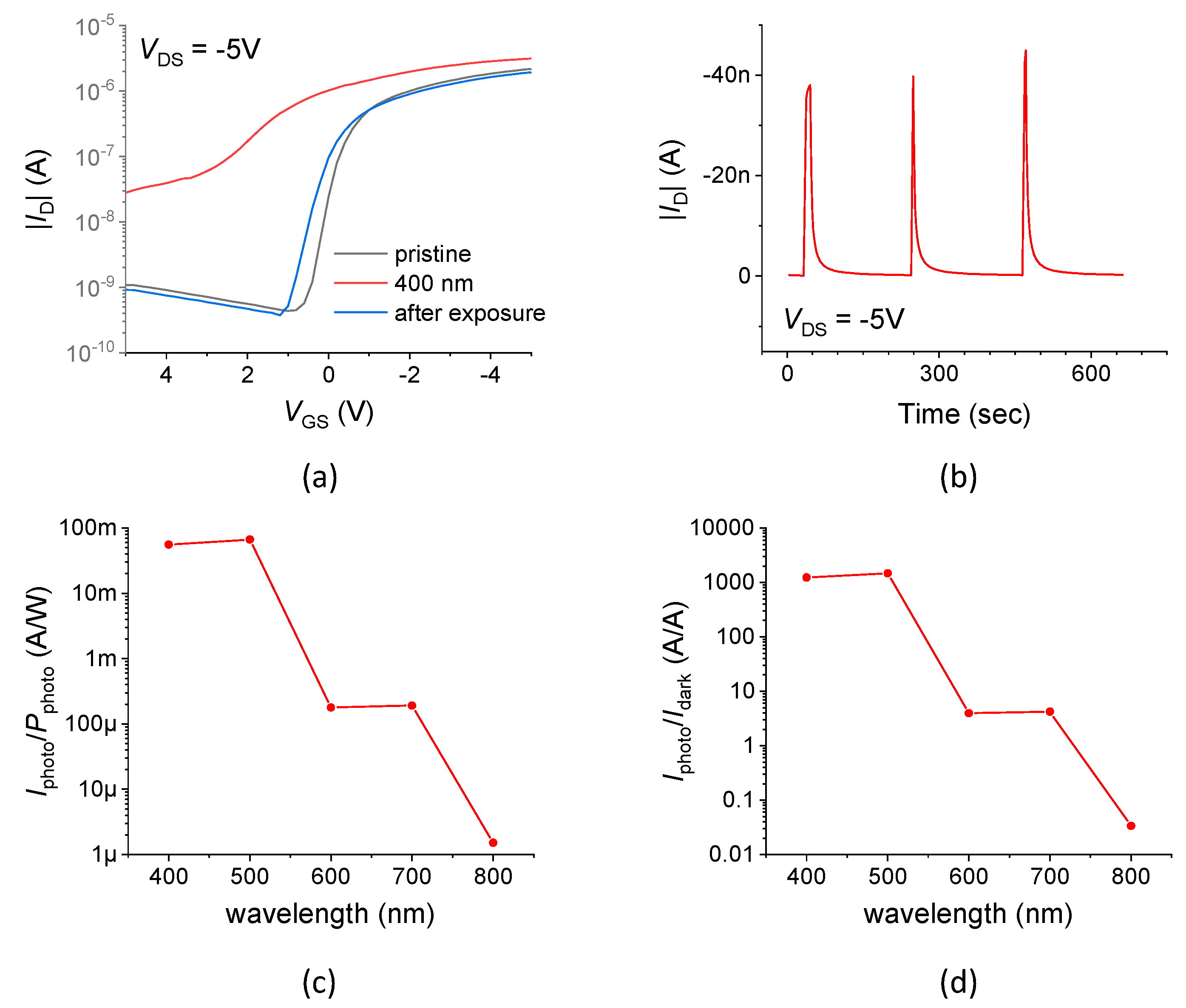
As a phototransistor, it is important that the device should have a good reproducibility before and after light illumination. As shown in
Figure 6a, the TIPS-pentacene OTFT could recover close to its pristine state, despite a positive shift of around 0.5 V observed in the transfer characteristics curves. Compared to the previously reported printed OTFTs for photodetection [
15], the recovery of the fabricated devices in this work seemed better, which could be explained by the reduced trap density in the printed OTFTs. Here, the transfer characteristics shift may be resulted from the slow recovery of the devices after light illumination with a time constant of 10.5 s, as shown in
Figure 6b. To improve this slow recovery issue, several studies have reported using gate pulses to instantly switch the phototransistors to the on-state and remove excess charge carriers [
16,
25]. The responsivity and sensitivity of the TIPS-pentacene OTFT was shown in
Figure 6c,d, respectively. For lights with shorter wavelengths, the values for responsivity and sensitivity were higher. In particular, the responsivity was 66.7 mA/W (
λ = 500 nm) and 55.9 mA/W (
λ = 400 nm), which are comparable to other reported organic phototransistors [
8]. The higher responsivity and sensitivity under exposure of lights with shorter wavelengths are attributed to larger photocurrents induced, as depicted in
Figure 5a. As seen in
Figure 6c,d, the responsivity and sensitivity were very low when the OTFT was exposed to light with the wavelength of 800 nm. For lights with the wavelengths of 600 nm and 700 nm, the responsivity and sensitivity were also not high, as only small changes were seen in the transfer characteristics (
Figure 4b). By characterizing the responsivity and sensitivity of the printed TIPS-pentacene OTFTs, one can understand the lights that the devices are most responsive and sensitive to and the shortcomings that need to be improved.
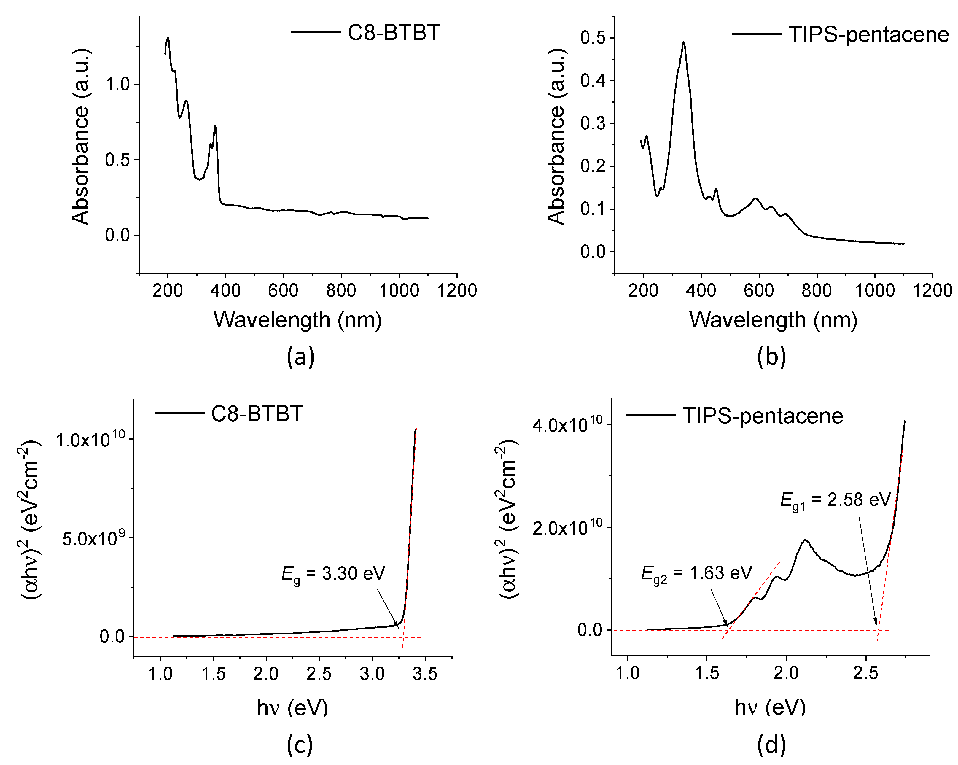
UV–vis spectroscopy was performed to understand the effect of light exposure to the two semiconductors. As shown in
Figure 7a, the UV-vis absorption spectrum of C8-BTBT indicated limited light absorbance in the wavelength range from 400 nm to 800 nm, and therefore excitons are not expected to be induced under these lights. In contrast, TIPS-pentacene has a significant increase in light absorbance from 750 nm to 600 nm wavelength lights, as seen in
Figure 7b. This could explain the reason that the TIPS-pentacene OTFTs had photoresponse to 700 nm wavelength light, but not 800 nm wavelength light. The absorption spectra for C8-BTBT and TIPS-pentacene were similar to the previous reports by other groups [
26,
27]. Note that, during the photoresponse characterizations for the fabricated OTFTs, the lights were applied from the top through the CYTOP layer; since CYTOP is a transparent material in the UV–vis–infrared spectra (at wavelengths of 200–2000 nm) [
28], the CYTOP encapsulation layer would not affect the absorption of visible lights by the semiconductors and therefore the photoresponse of the OTFTs. With the UV–vis absorption spectra, Tauc plots for the two semiconductors could be obtained and used to find their optical bandgaps. As shown in
Figure 7c, the optical bandgap of C8-BTBT was determined to be 3.30 eV, which is in the ultraviolet range. Therefore, the negligible photoresponse of C8-BTBT OTFTs to visible lights can be explained by that the photon energies of visible lights are not high enough to generate an exciton. From the Tauc plot shown in
Figure 7d, TIPS-pentacene has two optical bandgaps of 2.58 eV and 1.63 eV, which are corresponding to cutoff wavelengths of 481 nm and 761 nm. The larger optical bandgap (
Eg1) is more likely to be related to carrier generation by band-to-band transitions, whereas the smaller optical bandgap (
Eg2) is related to carrier generation by transitions involving forbidden-gap energy levels, due to the presence of sub-gap trap states of printed TIPS-pentacene thin films [
23]. These results suggest different semiconductor materials with smaller bandgaps need to be used to enhance the responsivity and sensitivity of the printed OTFTs to lights with longer wavelengths.
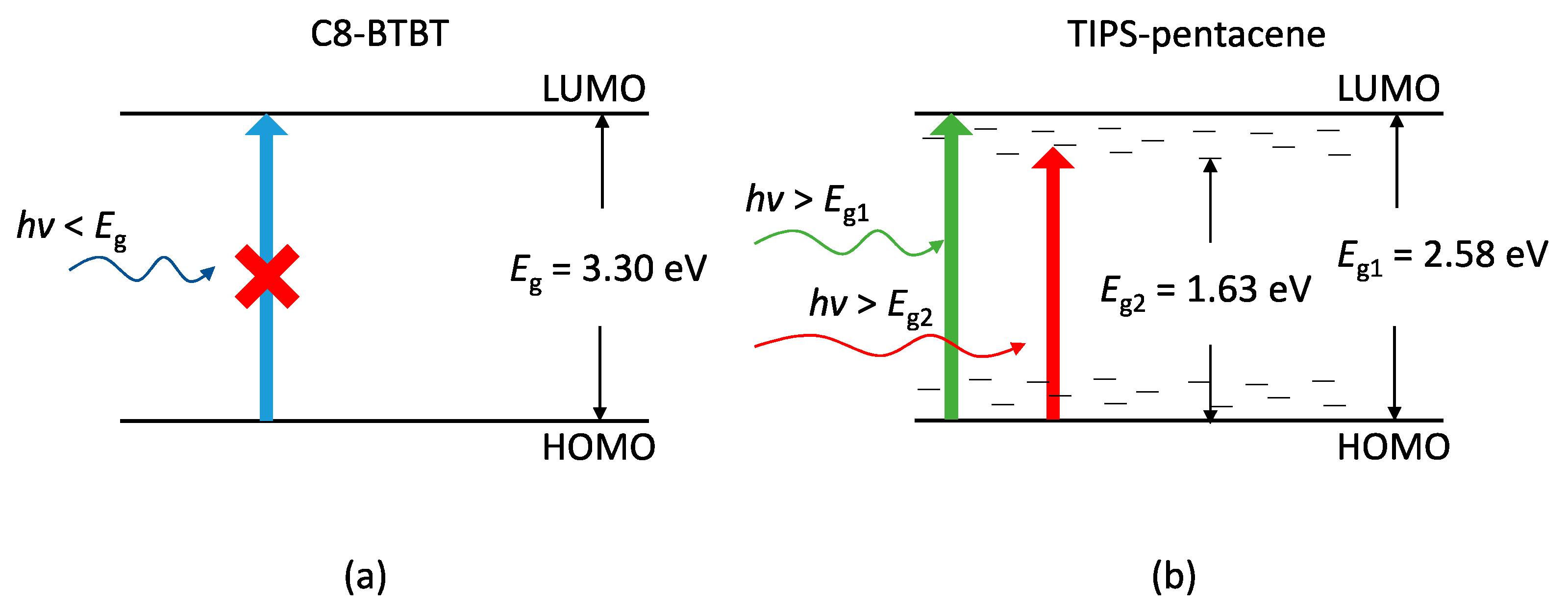
The mechanism of carrier generation under visible lights is depicted in
Figure 8. For C8-BTBT, since the photo energies of visible lights are lower than its optical bandgap, there are no carriers generated by visible light exposure. For TIPS-pentacene, the carriers generated under visible lights include band-to-band transitions and trap-assisted transitions: when the photon energy of exposing light is higher than
Eg2 but lower than
Eg1, the photocurrent was dominated by carriers generated by trap-assisted transitions; when the photon energy of exposing light is higher than
Eg1, the photocurrent was dominated by carriers generated by band-to-band transitions, as shown in
Figure 8b.
