Abstract
Macroscale modeling plays an essential role in simulating additive manufacturing (AM) processes. However, models at such scales often pay computational time in output accuracy. Therefore, they cannot forecast local quality issues like lack of fusion or surface roughness. For these reasons, this kind of model is never used for process optimization, as it is supposed to work with optimized parameters. In this work, a more accurate but still simple three-dimensional (3D) model is developed to estimate potential faulty process conditions that may cause quality issues or even process failure during the electron beam melting (EBM) process. The model is multilayer, and modeling strategies are developed to have fast and accurate responses. A material state variable allows for the molten material to be represented. That information is used to analyze process quality issues in terms of a lack of fusion and lateral surface roughness. A quiet element approach is implemented to limit the number of elements during the calculation, as well as to simulate the material addition layer by layer. The new material is activated according to a predefined temperature that considers the heat-affected zone. Heat transfer analysis accuracy is comparatively demonstrated with a more accurate literature model. Then, a multilayer simulation validates the model capability in predicting the roughness of a manufactured Ti6Al4V sample. The model capability in predicting a lack of fusion is verified under a critical process condition.
1. Introduction
Over the years, increased computing power combined with proper software development, has allowed for the implementation of simulation tools to speed up product development [1]. Chief among the numerous advantages offered by simulation is the possibility of investigating complex processes. Especially for new processes, such as additive manufacturing (AM), process simulation looks to be the best tool for processing complex understandings [2]. Electron beam melting (EBM) is an AM powder-bed process for metal components used for the production of end-usable parts in several industrial sectors [2]. During the EBM process, a high energy electron beam melts metallic powders by moving across the powder bed [3]. After the powder distribution, the whole powder bed is preheated. The preheating step establishes a uniform temperature on the powder bed, which is approximately equal to 60% of the melting point of the processed material. Except for a low helium flow (0.002 mbar) [4], the whole process occurs under vacuum to avoid beam deflection and to maintain a hot working environment. Thanks to the high working temperature and vacuum environment, EBM guarantees the possibility of manufacturing parts with high-quality materials such as intermetallic titanium alloys that cannot be processed with other AM or conventional processes [5]. Although the EBM process has great potential, the difficulties in controlling and determining proper process conditions limit the EBM application to niche industrial sectors. Process complexity is a result of numerous phenomena involved in the process [6], including the rapid material phase change [2]. The process conditions and implementation difficulties of process monitoring systems [2] make EBM attractive at the numerical scale. Figure 1 maps the relevant literature to an EBM simulation. Few models have adopted a mesoscopic approach in which particle to particle modeling is conducted [7,8,9,10,11]. The great level of detail included in powder modeling requires significant computational time and resources. Therefore, usually, only two-dimensional (2D) models were implemented. To reduce the computational time, most models in the literature are solved using the finite element (FE) method. In this case, the material is modeled as a continuum. FE models are mainly used to predict thermal distribution (pure thermal or uncoupled) [2,6,12,13,14,15,16,17,18,19,20,21,22]. These models simulated a single track or a single-layer and analyzed the process from a microscopic level (i.e., temperature distribution and melt pool size). Coupled models use a thermal solver coupled with at least one other solver. These models can be grouped into fully coupled thermomechanical [12,22,23,24,25,26,27,28], thermo-fluid flow [18,24,29], or weakly coupled [13,14]. A limited category of models analyzed the microscopic aspects of the process, such as the interaction between beam and powder particles [15,30,31], or even microstructural evolution [32]. Owing to the high number of elements that should be involved in the calculation, multilayer simulations have rarely been implemented [33] and instead have been primarily used for predicting residual stresses.
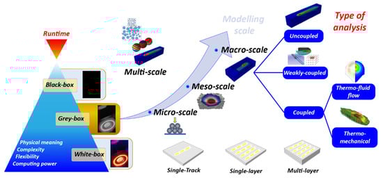
Figure 1.
Classification of electron beam melting (EBM) process simulation models.
Except for a few studies [15,16,23], calibrating coefficients were often applied to the heat source model to improve the match between experimental and simulation results. None of the reviewed FE models have explored the possibility of predicting the macroscopic process quality issues, i.e., the lack of fusion or surface roughness profile. As far as surface roughness is concerned, all developed models are empirical and can only estimate the average roughness value of the surface according to its angle with respect to the build platform [34]. S. Shrestha and K. Chou [35] developed a finite volume model based on a free surface approach to predict only the top surface roughness. However, the top surface is usually less critical than the vertical one because it shows better texture and a lower Ra value [34]. Typical values for vertical surface roughness range between 24 and 30 μm [36], while the Ra value of the top surfaces is around 6 μm [34]. Vertical surface roughness is mainly affected by the heat transfer effect between the molten material and the surrounding powder [34,37].
The prediction of macroscopic quality issues such as the lack of fusion and surface roughness profile over a short time is an important topic for simplifying the optimization process. This work presents a new and fast three-dimensional (3D) uncoupled thermal model for the multilayer simulation of the EBM process. The heat source is modeled following the approach developed in previous work [15], in which no calibrating coefficient was used. The multilayer simulation emulates the creation of the part layer by layer and the electron beam control along the hatching path and layer rotation. A material state variable is introduced to represent the material, which is melted during the process. This variable allows the identification of both the surface roughness profile and the lack of fusion. A new procedure is developed to reduce the calculation time, which accounts for a minimum number of elements during the calculation. This procedure is based on the quiet element approach, in which certain elements are activated only when necessary. This approach has been investigated in the literature to activate elements within a predefined volume by the time [38], such as the heat-affected zone (HAZ). However, the HAZ can vary in size and severity depending on the process condition and can be determined only by running experiments. A rough estimation of this quantity involves an incorrect number of elements that participate in the calculation and, therefore, a heat transfer analysis can be inaccurate or slow. To overcome this issue, the proposed procedure automatically considers element activation as a function of a predefined temperature. The activation temperature is determined by observing the HAZ predicted by the microscale model developed in a previous work [15]. The accuracy of the heat transfer analysis carried out with the proposed model, in terms of melt pool size and temperature distribution, is verified against the microscale model [15]. The capability of the proposed model in predicting the lateral roughness is validated by an experimental comparison. Herein, we verify the model response to a critical process parameter condition that causes a lack of fusion.
2. Materials and Methods
2.1. Modeling
Numerical modeling was based on the fundamentals presented in a previous study [15] in which a 3D microscale thermal model for the EBM process was developed. That work presented a new heat source model tailored according to the actual beam impact on the powder bed and new modeling for the powder thermal proprieties. The beam impact was simulated by Monte Carlo simulations. These simulations determined the effective beam diameter DE that mimics the electron distribution on the powder surface. The energy source model was, therefore, defined as a uniform heat distribution on a circular area in which a coefficient η depends on DE. This was used to couple the electron beam size with the uniform heat source. The material was modeled as a continuum, and the calculation of actual thermal conductivity of the powder considered both thermal radiation in the pores and heat transfer through the powder necks formed during preheating. The powder bed’s specific heat and latent heat of fusion were assumed to be equal to those of the solid bulk material [15,16]. The porosity of the powder material, φ, was considered equal to 0.32, which corresponds with a particle arrangement in body cubic centered (BCC) structure. Because of the thermal properties of the powder differ from the bulk (material after the melting) one, the powder was handled as different material, and during the melting simulation, a material change procedure updated the material properties from powder to bulk according to the achieved temperature. In that and subsequent works [15,16], the model was used to predict and validate the temperature distribution and melt pool size during the melting of a single track. Although the accuracy of this kind of modeling, the modeling of the actual EBM process should consider the melting of the entire layer and the addition of the material layer by layer. With this aim, the heat source developed in Reference [15] was adapted to consider the electron beam path across the powder bed. The heat source was, therefore, calculated according to the following equations:
where η is calculated according to the procedure [15], D is the whole simulation domain, and Γi is the domain of the flux application. The shape of Γi is circular and corresponds to the cross-section of the beam diameter. x1 and x2 are the coordinates of the nodes in the plane of the layer, while x3 is the coordinate along the build direction, which is the axis normal to the building platform (Figure 2). If nlayer is the total number of layers to be simulated, x3 varies layer after layer according to Equation (3).
The index n is the index of actual layer and ∆s is the layer thickness and thus an integer variable, which is calculated (Equation (4)) as the ratio between the total time increment, t, and time to scan a single layer, tlayer.
The beam movement over the x1x2 plane is governed by Equation (5) that describes the selection of the nodes that belong to the domain Γi in the x1x2 plane.
where Ø is the beam diameter and x1,inc and x2,inc are the incremental coordinates from the first position of the beam on the plane (x1c0, x2c0) and the last point of the scanning path. The beam is, therefore, moved point by point along a predefined scanning path. In this work, a standard single direction hatching strategy (Figure 2) was implemented. According to this strategy, the beam is moved with a constant speed, v, across the powder bed along parallel lines. The line offset parameter (LO) establishes the distance between the centerline of two adjacent lines, and all hatch melt lines are in the same direction. At each layer, the scanning path is rotated by 90 degrees clockwise. Therefore, x1,inc and x2,inc are calculated as follows:
where aii are the coefficients of an antisymmetric matrix that considered the single direction hatching and the scanning path rotation (Figure 2). The aii elements were calculated as follows:
In Equations (6) and (7), m is the line index and represents the actual line to be melted. The line index, m, was calculated from the time for the single line, ttracks, as follows:
Since the simulation here considered the melting of a square of side ltot, ttrack was calculated as follows:
q = ηUI/S (x1,x2,x3) ∈ Γi
q = 0 (x1,x2,x3) ∈ (D − Γi)
x3 = −(nlayer + n − 1)∆s
n = int(t/tlayer)
(x1 − x1,inc)2 + (x2 − x2,inc)2 ≤ (Ø/2)2
x1,inc = x1c0 + a12[v(t − ntlayer) − mttrack] + a11mLO
x2,inc = x2c0 + a22 [v(t − ntlayer) − mttrack] + a21mLO
a11 = a22 = −sin(nπ/2),
a12 = −a21 = cos(nπ/2).
m = int[(t − ntlayer)/ttrack]
ttrack = (ltot − Ø)/v
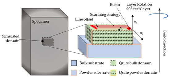
Figure 2.
Finite element (FE) model configuration.
The addition of the material layer by layer was emulated using a new element activation procedure based on the quiet element approach [33]. This method is a numerical approach used in FE simulation for processes that need to account for addition of material during the process. All elements of the model must be modeled from the beginning. Therefore, all elements within the workspace are assembled into the global thermal conductivity matrix, but the elements yet to be deposited are assigned ‘void’ material properties. Practically, the quiet elements are elements in which the thermal properties are adequately scaled and do not affect the calculation. The domain of analysis is progressively increased according to specific conditions. In this work, the quiet element approach was used not only to simulate the layer addition but also to keep the number of elements involved in the calculation into the current melted layer as low as possible. In this sense, the quiet elements confine the heat exchange only in the HAZ. This strategy is expected to increase the computational speed with respect to the literature models that consider the entire layer at the beginning of the simulation. This method uses a constant mesh and is simple. However, incorrect selection of elements to be eventually activated can lead to ill heat transfer. For this reason, a new criterion was implemented that aims to determine the lowest number of elements belonging to the HAZ without decreasing the accuracy of the heat transfer. Practically, this corresponds to determining the minimum temperature that refers to the location of the HAZ boundary at which the element must be “activated”. This temperature is called “activation temperature”. Element activation means changing the element material properties to the real ones. This methodology is called thermal activation because it depends exclusively on heat transfer. Since the nodal temperatures of a quiet element are different from those of an active element, body heat flux is numerically generated in some integration points to compensate for the temperature difference [39]. In this way, when the heat source moves, heat transfer can occur. This propagation generates a temperature field in the nodes of the quiet elements, which are constantly compared with the predefined activation temperature.
The determination of HAZ during the melting involves temperature monitoring and, therefore, experimental trials. To overcome these issues, the microscale model [15,16] was used to determine the HAZ, and thus the activation temperature. Firstly, few melting tracks are simulated using the microscale model. During the simulation, the minimum temperature that corresponds to the boundary of HAZ is identified. This temperature is set as activation temperature in the macroscale model, and the same simulation is performed. The results from the two models are compared in terms of temperature distribution and melt pool size. The macroscale model is then calibrated by changing the activation temperature iteratively until a good match between the two models is observed. With this approach, a trade-off between runtime, numerical convergence, and simulation accuracy is guaranteed. Several simulations at different process conditions showed that the activation temperature is slightly higher than the preheating temperature used in the model.
To further reduce the running time, material change was not considered. Therefore, the material properties were modeled directly as bulk material within the solid part are simulated. However, the material surrounding the external surfaces was modeled as powder material in order to account for the heat transfer between the melted and surrounding materials.
For each node of the model, a material state variable ID was defined to indicate the material’s temperature history. The material state was defined as “unmelted” (ID = 0) before the melting point was reached and as “melted” (ID = 1) after the melting point was reached. At the beginning of the process, all elements had an ID equal to zero. This variable, therefore, identified the material melted during the EBM process simulation from the one not melted. The melted material state (ID = 1) was used for both the liquid state and for all solid material in the model. The elements for which the ID was still equal to zero at the end of the process were identified as having a lack of fusion areas.
2.2. Model Implementation
The thermal model was implemented in Abaqus/Standard using user code subroutines for the heat source motion, element activation, and molten material representation. The whole domain is rather simple and consists of a solid substrate on which a set of layers are laid. To reduce the calculation time, the analysis domain used was a small portion of a specimen produced by EBM process with an external lateral surface in contact with a certain volume of loose powder. This powder volume was included to consider the heat exchange between the melted part and the surrounding area. The whole domain was divided into four subdomains (Figure 2): the bulk substrate, the powder substrate, the bulk quiet domain, and the quiet powder domain. The bulk substrate represented material already processed and not simulated in the analysis. The powder substrate was adjacent to the solid substrate. Therefore, a vertical surface of the bulk domain was numerically coupled with one surface of the powder domain. The other surfaces were considered adiabatic. The quiet bulk domain represented the domain scanned by the electron beam. It contained quiet elements that were activated once they achieved the activation temperature. The quiet powder domain represented a portion of material adjacent to the quiet bulk domain that was not scanned. This domain contained quiet elements that were automatically activated at the beginning of the layer and simulated heat transfer from the electron beam track and the surrounding powder. The quiet powder and bulk domains share a lateral surface. The other surfaces were considered adiabatic.
The mesh included DC3D8 (heat transfer brick) elements with a size equal to 0.05 mm in the quiet bulk and powder domains. The rest of the domain was discretized with a progressive coarsening mesh of up to 0.5 mm with DC3D4 elements (heat transfer tetrahedron).
The overall domain was subjected to a predefined field corresponding to the preheating temperature. To simulate the preheating step, the elements activated during the simulation had a preheating temperature.
According to the EBM melting strategy, the heat source swiped across the layer using a hatching mode. A specific user code, DFLUX, controlled the electron beam movement according to a user code that implemented the Equations from (1) to (11). Initially, the heat source moved at a constant speed along a certain axis. At each time increment, the code identified the nodes with the domain Γi and applied the heat flux according to Equations (1) and (2). After the scanning of a track, the heat source was repositioned at the origin of the previously scanned line. Then, it was translated perpendicularly to the previously scanned line and was of a quantity equal to LO. Hence, a new track was melted. The process was repeated until the layer was completed. Since only a portion of the whole cube was simulated, the code also considered the idle times due to the non-simulated portion of the layer.
To consider the melting strategy rotation, the scan lines were tilted on every layer by 90 degrees (Figure 2). Therefore, the code considered the heat source path rotation and its translation along the build direction. Both the path rotation and the translation were controlled by the time and the scanning speed.
The addition of the material during the simulation was implemented using the UEPACTIVATION VOL subroutine. This subroutine allows for the element activation control using rules predefined by the user. According to the thermal activation described in the previous paragraph, the elements are activated if the nodal temperature (T) is higher than the activation temperature (Tact). Owing to the Abaqus limitation, at the beginning of each layer, a few elements must be activated to trigger the subsequent thermal activation. Therefore, a predefined set of elements corresponding to the beam cross-section was activated by default at the beginning of each layer. This initial set was concentrically positioned at the center of the first beam spot. During subsequent increments, the elements were activated via the achieved temperature. Because of the heat propagation, it was possible that subsequent melting would determine the activation of elements belonging to the underlying layer if the temperature was higher than the activation temperature.
At the beginning of the simulation, the ID value at each node was equal to zero. At each increment, the ID was updated using the USDFLD subroutine. This user code identified and collected the nodes that had achieved the solidus temperature (TSolidus), while the temperature at the material point for each increment (T) was read using the GETVRM subroutine. Practically, all ID values were read at each node at the end of each increment, and the ID values equal to zero were updated (from 0 to 1) if the node achieved the melting point.
Figure 3 summarizes the FE whole structure implementation. Appendix B reports the source code of DFLUX and UEPACTIVATIONVOL subroutines as implemented in Abaqus.
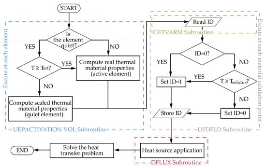
Figure 3.
FE model structure and the subroutine for the material addition (UEPACATIVATION VOL), the material state variable for the melted material (USDFLD), and heat flux application (DFLUX) implementations.
2.3. Model Validation
As mentioned above, the proposed model needs proper calibration before it can be run. The calibration is performed using the microscale model [15], named the reference model. Practically, the activation temperature in the macroscale model is iteratively changed until similar heat transfer conditions between the models are obtained.
First, to demonstrate the reliability of the heat transfer obtained via the proposed model after the calibration, a preliminary validation shows the comparison between the proposed and the reference models in terms of temperature distribution and melt pool size. This analysis considered the melting of a portion of a single layer. Then, further validation evaluates the ability of the model to predict the lateral surface roughness. In this case, a multilayer simulation was performed and compared with the experimental data.
In order to give a measure of the computational time, all simulations were performed on a personal computer with the following specifications: Intel® Core ™ i7-8700K 3.70 GHz processor, 32 GB RAM, and 1 TB SSD. A six-core parallelization was used according to the computational resources used to perform the analysis.
2.3.1. Comparison with the Reference Model: Single Layer Validation
This validation was carried out by simulating the melting of a single layer, 30 mm × 30 mm, of Ti-48Al-2Cr-2Nb alloy. The layer was 0.090 mm thick. The material properties for the bulk material were extracted from Reference [40], while the powder proprieties were calculated from the bulk one according to Reference [15]. The material properties implemented in the model were reported as Supplementary Materials. The simulation by the proposed and reference models consisted of the melting of six unidirectional parallel scan tracks. Table 1 lists the process parameters used for both simulations. The comparison considered both the melt pool size and temperature distribution.

Table 1.
Simulation parameters for both analyses.
2.3.2. Multilayer Experimental Validation
The experiment consisted of producing a 10 mm × 10 mm × 20 mm-sized parallelepiped sample made on Ti6Al4V. The sample was produced using an Arcam A2X, standard Arcam powder (average particle size equal to 75 μm) with a layer thickness equal to 0.050 mm. The process parameters are listed in Table 2. According to the standard melting strategy, the melting strategy consisted of unidirectional parallel lines with a clockwise rotation of 90 degrees every layer (Figure 2). After the production, the sample was cleaned by loose powder. The 2D surface roughness profiles of the lateral surface samples were acquired using an RTP-80 profilometer, equipped with a TL90 drive unit. The cut-off length and sampling length were chosen according to ISO 4288:1997. For each lateral surface of the sample, the roughness profile was measured along the build direction. Additionally, for each surface, three profiles were collected: one on the center of the specimen and the other two equally spaced from the first one and from the sample’s edges. The collected profiles for each surface are reported in Appendix A, while all collected data and roughness descriptors can be found in the database [41]. The average roughness (Ra) and root mean square (Rq) values were equal to 28 µm and 33 μm, respectively.
Table 2.
Process parameters for the experiment and simulation.
The numerical simulation by the proposed model emulated the experimental setup. The material properties for Ti6Al4V were extracted from a prior study [15]. The layer was fixed to be equal to 0.050. Figure 2 shows the portion of the simulated specimen. The simulated portion of the cube was 2.2 mm × 2 mm × 1.5 mm. As described above, the analysis domain consisted of four subdomains. The quiet bulk domain contained 10 layers (soft green with black dotted edges in Figure 2) that were added over a solid substrate (soft blue with black edges in Figure 2). The powder substrate (soft blue with orange edges) shared a lateral surface with the solid substrate, while the quiet powder domain (soft green with orange dotted edges in Figure 2) was located over the powder substrate and adjacent to the quiet bulk domain. According to the proposed procedure, at the beginning of each layer, the initial activated area was cylindrical and concentric to the initial position of the beam. The height of the cylinder was set to be equal to the layer thickness, and its diameter was equal to the beam diameter. The video of the simulation after the model calibration is provided as Supplementary Materials.
3. Results and Discussion
3.1. Model Validation
3.1.1. Single-Layer Simulation Validation
As mentioned above, the reliability of the proposed model response was compared with the reference one in terms of melt pool dimensions and maximum temperature (Tmax). The length (l), the width (w), and the depth (d) of the melt pool were measured. The activation temperature was fine-tuned to a convergence in the heat transfer between the two models. The model was considered calibrated when small deviations were observed between the two models. For an activation temperature equal to 1700 K, the deviations from the reference model are reported in Table 3. This deviation can be attributed to the different material properties attributed to the layer. The reference model, in fact, considered the simulation of the entire layer with the powder thermal material properties that were then updated from powder to bulk according to the achieved temperature during the process. In the proposed model, the portion of the layer to be melted was modeled directly as bulk material. Because of that, deviations were more significant in the first track. In this case, the beam should melt a track surrounded completely by material with low conductivity (powder), while in the proposed model, the powder was modeled only on one side of the beam track. In subsequent passages, the beam overlapped with a portion of the already solidified bulk material, and the deviation between the two models was, therefore, lower, as shown in the third scanning line (Table 3). The difference in the melt pool depth remained, implying that there was an overestimation of the heat penetration in the proposed model. However, the penetration depth was also affected by uncertainty due to the substrate temperature after melting, which could not have been forecasted with a single-layer simulation.
Table 3.
Single-layer validation: the deviations between the reference model against the proposed model in terms of the melt pool dimension and maximum temperature.
Overall, the numerical results obtained adopting the new modeling approach can be considered to be consistent with the reference model.
Additionally, using the same computational resources, the total simulation with the reference model took around 8 CPU hours, while the same simulation with the proposed model after calibration took around 5 h. Therefore, the proposed approach to the EBM modeling with proper calibration of the activation temperature allows to obtain an accurate enough heat transfer simulation and a significant runtime saving of about 40% with respect to the reference model.
3.1.2. Lateral Surface Roughness Prediction
According to the proposed approach, firstly, few melting lines were simulated using both the reference and the proposed models. Then, the proposed model was calibrated by changing the activation temperature iteratively until a heat transfer convergence between the two models. For an activation temperature equal to 1000 K, the obtained numerical results from the calibrated model showed a small deviation in comparison with the corresponding reference model measurements. For this reason, the activation temperature was set equal to 1000 K.
To be numerically consistent with the experiment, the surface roughness was described by the surface profile between the quiet bulk and powder domains, considering the melted material. This information was extracted by the material state variable ID. As mentioned above, the ID was equal to 1 if the node achieved the solidus temperature, otherwise, it remained equal to zero. Graphically, this result can be represented by a colorful map in which the elements in red were an ID equal to 1 and those in blue were an ID equal to zero. Figure 4 shows the experimental 2D roughness profile (blue line) overlapped with the numerical one. The numerical profile was obtained using a cross-section of the model. The surface roughness profile of the sample (blue line) was characterized by peaks and valleys, which were repeated with a certain frequency. This frequency seems to be linked to the rotation layer and, therefore, to a distance equal to four layers. This frequency was also observed in the numerical results. The peaks of the numerical simulation appeared to be representative of the experimental ones, while the numerical valleys appeared to be more profound. This could be explained by the presence of powder particles attached to the experimental surface because of the high sintering level [42,43]. These particles could not be removed during cleaning because they were partially melted into the surface. Since the simulation approach used the FE method and a continuum domain, the presence of these particles was not detected.
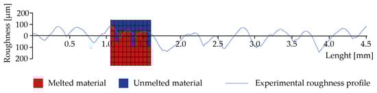
Figure 4.
Comparison between the numerical and experimental roughness profiles.
The differences of the wave width between the experimental and the numerical profiles can be explained by the effective layer thickness [12], which was around 2 or 3 times larger than the lowering of the build platform [23] and was not considered in this simulation.
A certain effect may also be caused by the material change, which was not considered in the simulation and may increase the heat transfer toward the powder domain because of the local thermal conductivity change.
Overall, the numerical simulation appeared to represent the actual surface profile well and established the capability of the model to give information about the surface texture resulting from the EBM process.
Figure 5 shows a portion of the 3D profile of the lateral surface obtained using numerical simulation. This profile was obtained by manipulating the numerical output visualization to show the boundary surface between the melted and unmelted material. Figure 5 detects the peaks and valleys along the surfaces previously observed in both 2D experimental and numerical profiles.
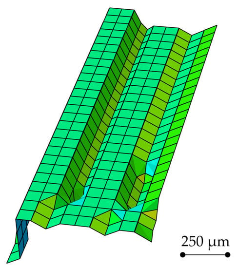
Figure 5.
3D numerical surface profile: peaks and valleys can be observed.
To estimate the average roughness (Ra) and the root mean square (Rq) of the surface and to increase the sampling length in the model, a longer simulation was performed up to 17 layers, which corresponds to the height of the simulated sample equal to 0.85 mm. From this simulation, Ra and Rq resulted in being equal to 35 µm and 42 µm, respectively (see Appendix A for details). The obtained values are comparable with the experimental one (Ra = 28 µm and Rq = 33 μm). Therefore, the results obtained from the model are believed to serve as good indicators of the lateral surface profiles. However, as will be discussed in the Conclusion, a more detailed investigation of both experimental and simulated melting is planned.
3.2. Lack of Fusion in EBM Process
Given the results presented in Section 3.1.2, further analysis was carried out to evaluate the model response in predicting the lack of fusion under a critical process condition. Lack of fusion occurs easily if the EBM conditions are not appropriate. For instance, an increased line offset toward beam diameter results in lower energy densities, which causes a lack of fusion [44]. With this scope, the line offset of the previous multilayer simulation was increased up to 0.800 mm, which was approximately equal to the beam diameter (Table 2). The other parameters remained constant, including the activation temperature.
Numerically, the lack of fusion was represented by those elements named “unmelted material” and, therefore, did not achieve the melting point during the simulation. The ID variable gathered the state of the element. As before, within the quiet bulk domain, the unmelted elements (ID = 0) were plotted in blue (Figure 6), while the melted elements (ID = 1) were plotted in translucent. As can been seen, Figure 6 shows the presence of numerous lack-of-fusion areas entrapped in the solid material. The locations of these unmelted areas look to be dependent on the layer rotation strategy. The simulation, therefore, identified this process condition as faulty. In fact, larger line offset values that did not allow for the full melting of the material, causing the lack of fusion appearance, voids, and porosities, thus inhibiting the continuation process [18].
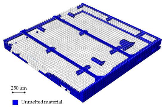
Figure 6.
Simulation of a process condition that causes the appearance of a lack of fusion. The translucent elements indicate the material that achieved the melting point during the process (ID = 1), while blue ones indicate the material that has never achieved the melting point (ID = 0). After the cooling phase, the unmelted material during the process represents a lack-of-fusion defect in the final part.
3.3. Runtime Considerations
The total duration of the 10-layer simulation was around 20 h. The process simulation with a larger line offset took around 2 h.
A convergence analysis was carried out on mesh size during the activation temperature calibration. The mesh size was finer than 0.050 mm and significantly increased the runtime without increasing the output accuracy. Lower activation temperatures lead to the activation of a higher number of elements, therefore, worsening the runtime. Higher temperatures caused the non-convergence of the model because of the incorrect heat transfer.
4. Conclusions
The literature review of multilayer simulations for the EBM process and more in general for AM processes is poor and did not allow the prediction of the local quality. In this work, an accurate but simple 3D multilayer model was developed for the optimization of process parameters. The aim of the model was to rapidly identify a set of potentially faulty process conditions. To speed up the runtime, we developed a new tailor-made procedure. This procedure was based on the progressive element activation under a specific temperature, which was used not only to simulate the layer by layer production but also to limit the number of elements that participated in the calculation during the single-layer melting. The activation temperature was determined by accurately analyzing the HAZ simulation using a microscale model that predicted the temperature distribution and the actual melt pool. The activation temperature was calibrated, and a small difference in heat transfer was observed between the two models.
To identify the quality inherent in the lack of fusion, our methodology included the definition of a material state variable (ID), which allowed us to distinguish between melted and unmelted material. The graphical visualization of ID evaluated the roughness profile of a sample surface along a build direction, as well as the lack of fusion appearance. For validation purposes, the comparison between the microscale model used for the activation temperature calibration and the proposed one was shown. Successively, the model’s ability to predict surface texture was verified against experimental results. The model response was tested under a critical condition that, in real production, generated a process failure. The right activation temperature led to a small deviation between the microscale and the proposed models in terms of heat transfer with a savings time of about 40%. The model showed good agreement with the experimental and numerical measurements in forecasting the 2D surface profile and the roughness descriptors (Ra and Rq). The little deviation between the experimental and the numerical demonstrates that the proposed approach will be an efficient model for simulating the roughness profile. However, a more detailed numerical analysis will be carried out for the verification of the model capability in roughness prediction at different process conditions. Additionally, further work will consider implementing the effect on the powder layer due to account both for thermal expansion of powder particles and for porosity reduction of the powder bed during the heating [23].
The model also demonstrated the ability to predict a lack of fusion associated with thermal effects due to, for example, a large line offset. In such a case, with respect to the experimental trial, the simulation allowed for hugely significant time-saving process optimization. From this point of view, the presented results demonstrated that the proposed approach could be easily applied to the process development stage in order to reject faulty process conditions. From an industrial point of view, this approach can save time and resources with respect to the experimental routine. Further model validations and developments with the aim of simulating complex parts may help in the production of defect-free parts. Additionally, an accurate prediction of surface profile roughness may allow for the identification of minimum allowances, which are needed to add for the subsequent finishing operations. Moreover, there is a need for microcrack identification, which can jeopardize a product’s fatigue limits.
Supplementary Materials
The following are available online at https://www.mdpi.com/2073-4352/10/6/532/s1, S1: Video: Multilayer process simulation of the EBM process for Ti-6Al-4V: the size of the simulated domain of material addition is 2.2 mm × 2 mm × 1.5 mm. The domain contains 10 layers with a layer thickness equal to 0.050 mm. The process parameters are: beam diameter = 0.780 mm; Line offset = 0.200 mm; scan speed = 471.69; Heat flux = 347.920 W/mm^2; Preheat temperature = 923 K. The movie shows the temperature distribution evolution over the time (on the right) and the corresponding melted material (on the left). S2: Thermal material properties for Ti-48Al-2Cr-2Nb implemented in the simulation.
Author Contributions
Conceptualization, M.G.; data curation, M.G. and O.D.M.; investigation, M.G. and O.D.M.; methodology, M.G.; resources, L.I.; software, M.G. and O.D.M.; supervision, L.I.; validation, M.G. and O.D.M.; visualization, M.G. and O.D.M.; writing—original draft, O.D.M.; writing—review and editing, M.G. All authors have read and agreed to the published version of the manuscript.
Funding
This research received no external funding.
Conflicts of Interest
The authors declare no conflict of interest.
Appendix A. Experimental and Numerical Roughness Profile and Ra and Rq Calculation
Figure A1 depicts all surface roughness collected during the experiments. For each surface of the sample, the roughness profiles have been acquired along the build direction and replicated three times. The first profile was acquired along the surface center, while the other two profiles were equally spaced from the first one and the edges of the sample. These measurements were collected and indexed as follows: the first number (from 1 to 4) indicates the index of the surface; the second number (from 1 to 3) specifies the measure replica. The surface roughness profiles of the sample were acquired using an RTP-80 profilometer, equipped with a TL90 drive unit. The cut-off length and sampling length were chosen according to ISO 4288:1997.

Figure A1.
Surface roughness profiles from each surface. The measurements have been replicated three times. The first number (from 1 to 4) indicates the index of the surface; the second number (from 1 to 3) specifies the measure replica.
For each measurement, the parameters Ra and Rq and the surface profile were also collected. The average value of the Ra and Rq was equal to 28 µm and 33 μm, respectively. All collected measurements and roughness descriptors can be found in the database [41].
A portion of the samples has been simulated numerically according to the proposed methodology. In order to have a significant and reliable number of roughness values to calculate the predicted Ra and Rq values, the addition of 17 layers over a solid substrate has been simulated. According to the methodology presented in the paper, the boundary between the unmelted and the melted materials has been extracted from the simulation results by using the ID variable (Figure A2a). According to the standard [45], Ra is calculated, over the evaluation length, as the arithmetical mean of the absolute values of the profile heights (yi) from the mean line of the effective profile. The mean line is the line having the shape of the geometrical profile and dividing the effective profile (Figure A2) so that within the sampling length, the sum of the squares of the distances between the effective profile points and the mean line is minimum. Analogously, Rq is the root mean square average of the profile heights over the evaluation length. From the numerical model, Ra and Rq resulted in being equal to 35 µm and 42 µm, respectively.

Figure A2.
Numerical measurements of the surface roughness: (a) cross-section of the model that shows the ID state variable map (b) Numerical profile and its mean line for Ra calculation.
Appendix B. Source Code Listing of DFLUX and UEPACTIVATIONVOL Subroutines as Implemented in Abaqus
Appendix B lists the user code as written in Abaqus to implement the modeling as discussed in the main paper. The subroutines are in FORTRAN language.
SUBROUTINE DFLUX(FLUX,SOL,KSTEP,KINC,TIME,NOEL,NPT,COORDS, JLTYP,TEMP,PRESS,SNAME)
INCLUDE ‘ABA_PARAM.INC’
DIMENSION FLUX(2), TIME(2), COORDS(3)
CHARACTER*80 SNAME
c
ltot = 10 !scan track lenght
D = 0.78 !beam diameter
V = 471.69 !beam speed
Q = 347920 !heat flux magnitude
LO = 0.2 !line offset
LT = 0.05 !layer thickness
n_layer = 10 !number of layers
c
x1 = COORDS(3) !spatial coordinate x1
x2 = COORDS(1) !spatial coordinate x2
x3 = COORDS(2) !spatial coordinate x3
t = TIME(1) !total time
c
x1c0 = 0 !coordinates of the first position of the beam
x2c0 = −D/2 !coordinates of the first position of the beam
c
t_track = (ltot-D)/v !time to perform a single line
t_layer = ltot/LO*t_track !time to scan a single layer, tlayer
c
n = int(t/t_layer) !layer index
m = int((t-n*t_layer)/t_track) !line index
c
a11 = −sin(n*(pi/2)) !matrix coefficients
a22 = −sin(n*(pi/2))
a12 = cos(n*(pi/2))
a21 = −cos(n*(pi/2))
c
x1_inc = x1c0 + a12*(v*(t-n*t_layer)-m*t_track) + a11*m*LO !incremental coordinates from x1c0 and the last point of the scanning path
x2_inc = x2c0 + a22*(v*(t-n*t-layer)-m*t_track) + a21*m*LO !incremental coordinates from x2c0 and the last point of the scanning path
c
if(x3.EQ.-(n_layer + n − 1)*LT)then !check the x3
if ((x1-x1_inc)**2 + (x2−x2_inc)**2.LE.(D/2)**2)then
FLUX(1) = q !Heat source application. Since only a portion of the whole cube was simulated,
end if !was considered the idle times due to the non-simulated portion of the layer
end if
c
RETURN
END
c
subroutine UEPACTIVATIONVOL(lFlags, epaName, noel, nElemNodes, iElemNodes, mcrd, coordNodes, uNodes, kstep, kinc, time, dtime, temp, npredef, predef, nsvars, svars, sol, solinc, volFract, nVolumeAddEvents, volFractAdded, csiAdded)
include ‘aba_param.inc’
character*80 epaName
c
ltot = 10 !scan track lenght
D = 0.78 !beam diameter
V = 471.69 !beam speed
LO = 0.2 !line offset
LT = 0.05 !layer thickness
n_layer = 10 !number of layers
Tact = 1000 !activation temperature
c At the beginning of the simulation the status of all elements must be set as “quiet”
volFractAdded(1) = 0.d0
t = TIME(1) !total time
x1 = coordNodes(3,1) !spatial coordinate x1
x2 = coordNodes(1,1) !spatial coordinate x2
x3 = coordNodes(2,1) !spatial coordinate x3
c
x1c0 = 0 !coordinates of the first position of the beam
x2c0 = −R !coordinates of the first position of the beam
n = int(t/t_layer) !layer index
c Activation of the initial set of elements
if(x3.EQ.-(n_layer+n-1)*LT)then
if ((x1-x1c0)**2+(x2-x2c0)**2.LE.(D/2)**2)then
volFractAdded(1) = 1.d0
end if
end if
c Thermal activation
if (x3.LE.-(n_layer+n-1)*LT)then
if(sol(1).GE. Tact) then
end if
end if
c
return
end
References
- Dilberoglu, U.M.; Gharehpapagh, B.; Yaman, U.; Dolen, M. The role of additive manufacturing in the era of industry 4.0. Procedia Manuf. 2017, 11, 545–554. [Google Scholar] [CrossRef]
- Galati, M.; Iuliano, L. A literature review of powder-based electron beam melting focusing on numerical simulations. Addit. Manuf. 2018, 19, 1–20. [Google Scholar] [CrossRef]
- Gaytan, S.M.; Murr, L.E.; Medina, F.; Martinez, E.; Lopez, M.I.; Wicker, R.B. Advanced metal powder based manufacturing of complex components by electron beam melting. Mater. Technol. 2009, 24, 180–190. [Google Scholar] [CrossRef]
- Markl, M.; Lodes, M.; Franke, M.; Körner, C. Additive manufacturing using selective electron beam melting. Weld. Cut. 2017, 16, 177–184. [Google Scholar]
- Baudana, G.; Biamino, S.; Ugues, D.; Lombardi, M.; Fino, P.; Pavese, M.; Badini, C. Titanium aluminides for aerospace and automotive applications processed by Electron Beam Melting: Contribution of Politecnico di Torino. Met. Powder Rep. 2016, 71, 193–199. [Google Scholar] [CrossRef]
- Sigl, M.; Lutzmann, S.; Zaeh, M.F. Transient physical effects in electron beam sintering. In Proceedings of the 17th Solid Freeform Fabrication Symposium SFF 2006, Austin, TX, USA, 14–16 August 2006; pp. 464–477. [Google Scholar]
- Attar, E. Simulation of Selective Electron Beam Melting Processes. Ph.D. Thesis, Friedrich-Alexander-Universität Erlangen-Nürnberg (FAU), Erlangen, Alemanha, 2011. [Google Scholar]
- Ammer, R.; Markl, M.; Ljungblad, U.; Körner, C.; Rüde, U. Simulating fast electron beam melting with a parallel thermal free surface lattice Boltzmann method. Comput. Math. Appl. 2014, 67, 318–330. [Google Scholar] [CrossRef]
- Ammer, R.; Rüde, U.; Markl, M.; Körner, C. Modeling of Thermodynamic Phenomena with Lattice Boltzmann Method for Additive Manufacturing Processes. In Proceedings of the 23rd International Conference on Discrete Simulation of Fluid Dynamics (DSFD), Paris, France, 28 July–1 August 2014. [Google Scholar]
- Klassen, A.; Forster, V.E.; Körner, C. A multi-component evaporation model for beam melting processes. Model. Simul. Mater. Sci. Eng. 2017, 25, 025003. [Google Scholar] [CrossRef]
- Yan, W.; Qian, Y.; Ge, W.; Lin, S.; Liu, W.K.; Lin, F.; Wagner, G.J. Meso-scale modeling of multiple-layer fabrication process in selective electron beam melting: Inter-layer/track voids formation. Mater. Des. 2018, 141, 210–219. [Google Scholar] [CrossRef]
- Riedlbauer, D.; Scharowsky, T.; Singer, R.F.; Steinmann, P.; Körner, C.; Mergheim, J. Macroscopic simulation and experimental measurement of melt pool characteristics in selective electron beam melting of Ti-6Al-4V. Int. J. Adv. Manuf. Technol. 2016, 88, 1–9. [Google Scholar] [CrossRef]
- Koepf, J.A.; Soldner, D.; Ramsperger, M.; Mergheim, J.; Markl, M.; Körner, C. Numerical microstructure prediction by a coupled finite element cellular automaton model for selective electron beam melting. Comput. Mater. Sci. 2019, 162, 148–155. [Google Scholar] [CrossRef]
- Soldner, D.; Mergheim, J. Thermal modelling of selective beam melting processes using heterogeneous time step sizes. Comput. Math. Appl. 2019, 78, 2183–2196. [Google Scholar] [CrossRef]
- Galati, M.; Iuliano, L.; Salmi, A.; Atzeni, E. Modelling energy source and powder properties for the development of a thermal FE model of the EBM additive manufacturing process. Addit. Manuf. 2017, 14, 49–59. [Google Scholar] [CrossRef]
- Galati, M.; Snis, A.; Iuliano, L. Experimental validation of a numerical thermal model of the EBM process for Ti6Al4V. Comput. Math. Appl. 2018, 78, 2417–2427. [Google Scholar] [CrossRef]
- Qi, H.B.; Yan, Y.N.; Lin, F.; Zhang, R.J. Scanning method of filling lines in electron beam selective melting. Proc. Inst. Mech. Eng. Part B J. Eng. Manuf. 2007, 221, 1685–1694. [Google Scholar] [CrossRef]
- Zäh, M.F.; Lutzmann, S. Modelling and simulation of electron beam melting. Prod. Eng. 2010, 4, 15–23. [Google Scholar] [CrossRef]
- Shen, N.G.; Chou, K. Thermal Modeling of Electron Beam Additive Manufacturing Process Powder Sintering Effects. In Proceedings of the Asme International Manufacturing Science and Engineering Conference, Notre Dame, IN, USA, 4–8 June 2012; American Society of Mechanical Engineers: New York, NY, USA, 2012; pp. 287–295. [Google Scholar]
- Tolochko, N.K.; Arshinov, M.K.; Gusarov, A.V.; Titov, V.I.; Laoui, T.; Froyen, L. Mechanisms of selective laser sintering and heat transfer in Ti powder. Rapid Prototyp. J. 2003, 9, 314–326. [Google Scholar] [CrossRef]
- Sih, S.S.; Barlow, J.W. Emissivity of powder beds. In Proceedings of the Solid Freeform Fabrication Symposium, Austin, TX, USA, 1995; The University of Texas at Austin: Austin, TX, USA; Volume 6, pp. 7–9.
- Cheng, B.; Price, S.; Lydon, J.; Cooper, K.; Chou, K. On Process Temperature in Powder-Bed Electron Beam Additive Manufacturing: Model Development and Validation. J. Manuf. Sci. Eng. ASME 2014, 136, 1–12. [Google Scholar] [CrossRef]
- Galati, M.; Snis, A.; Iuliano, L. Powder bed properties modelling and 3D thermo-mechanical simulation of the additive manufacturing Electron Beam Melting process. Addit. Manuf. 2019, 30, 100897. [Google Scholar] [CrossRef]
- Jamshidinia, M.; Kong, F.; Kovacevic, R. Temperature distribution and fluid flow modeling of electron beam melting® (EBM). In Proceedings of the ASME International Mechanical Engineering Congress and Exposition, Proceedings (IMECE), Houston, TX, USA, 9–15 November 2012. [Google Scholar]
- Jamshidinia, M.; Kong, F.; Kovacevic, R. The Coupled CFD-FEM Model of Electron Beam Melting® (EBM). In Proceedings of the ASME District F-Early Career Technical Conference Proceedings ASME District F-Early Career Technical Conference, ASME District F–ECTC 2013, Birmingham, AL, USA, 2–3 November 2013. [Google Scholar]
- Vastola, G.; Zhang, G.; Pei, Q.X.; Zhang, Y.-W. Controlling of residual stress in additive manufacturing of Ti6Al4V by finite element modeling. Addit. Manuf. 2016, 12, 231–239. [Google Scholar] [CrossRef]
- Shen, N.; Chou, K. Simulations of Thermo-Mechanical Characteristics in Electron Beam Additive Manufacturing. In Proceedings of the ASME 2012 International Mechanical Engineering Congress and Exposition, Houston, TX, USA, 9–15 November 2012; American Society of Mechanical Engineers: New York, NY, USA, 2012; pp. 67–74. [Google Scholar]
- Cheng, B.; Chou, K. Geometric consideration of support structures in part overhang fabrications by electron beam additive manufacturing. Comput. Des. 2015, 69, 102–111. [Google Scholar] [CrossRef]
- Jamshidinia, M.; Kong, F.; Kovacevic, R. Numerical modeling of heat distribution in the electron beam melting® of Ti-6Al-4V. J. Manuf. Sci. Eng. 2013, 135, 61010. [Google Scholar] [CrossRef]
- Yan, W.; Liu, W.K.; Lin, F. An effective Finite Element heat transfer model for Electron Beam Melting An effective Finite Element heat transfer model for Electron Beam Melting process. In Proceedings of the Advances in Materials and Processing Technologies Conference, Madrid, Spain, 14–18 December 2015. [Google Scholar]
- Yan, W.; Ge, W.; Smith, J.; Lin, S.; Kafka, O.L.; Lin, F.; Liu, W.K. Multi-scale modeling of electron beam melting of functionally graded materials. Acta Mater. 2016, 115, 403–412. [Google Scholar] [CrossRef]
- Olanipekun, A.T.; Abioye, A.A.; Emmanuel, K. Time-Dependent Ginzburg—Landau equation modelling of electron beam additive manufactured Titanium alloy. Leonardo Electron. J. Pract. Technol. 2018, 32, 93–102. [Google Scholar]
- Michaleris, P. Modeling metal deposition in heat transfer analyses of additive manufacturing processes. Finite Elem. Anal. Des. 2014, 86, 51–60. [Google Scholar] [CrossRef]
- Galati, M.; Minetola, P.; Rizza, G. Surface Roughness Characterisation and Analysis of the Electron Beam Melting (EBM) Process. Materials 2019, 12, 2211. [Google Scholar] [CrossRef] [PubMed]
- Shrestha, S.; Chou, K. A build surface study of Powder-Bed Electron Beam Additive Manufacturing by 3D thermo-fluid simulation and white-light interferometry. Int. J. Mach. Tools Manuf. 2017, 121, 37–49. [Google Scholar] [CrossRef]
- Ek, R.K.; Rännar, L.E.; Bäckstöm, M.; Carlsson, P. The effect of EBM process parameters upon surface roughness. Rapid Prototyp. J. 2016, 22, 495–503. [Google Scholar]
- Koike, M.; Martinez, K.; Guo, L.; Chahine, G.; Kovacevic, R.; Okabe, T. Evaluation of titanium alloy fabricated using electron beam melting system for dental applications. J. Mater. Process. Technol. 2011, 211, 1400–1408. [Google Scholar] [CrossRef]
- Piscopo, G.; Atzeni, E.; Salmi, A. A hybrid modeling of the physics-driven evolution of material addition and track generation in laser powder directed energy deposition. Materials 2019, 12, 2819. [Google Scholar] [CrossRef]
- SIMULIA User Assistance 2019—Progressive Element Activation. Available online: https://help.3ds.com/2019/English/DSSIMULIA_Established/SIMACAEANLRefMap/simaanl-c-elemactivation.htm?ContextScope=all (accessed on 9 April 2020).
- Cagran, C.; Wilthan, B.; Pottlacher, G.; Roebuck, B.; Wickins, M.; Harding, R.A. Thermophysical properties of a Ti–44%Al–8%Nb–1%B alloy in the solid and molten states. Intermetallics 2003, 11, 1327–1334. [Google Scholar] [CrossRef]
- Galati, M.; Di Mauro, O. Numerical prediction of surface roughness of as-built electron beam melting parts: Experimental data 2020. Available online: https://data.mendeley.com/datasets/cgwvch6kn8/1 (accessed on 16 June 2020).
- Triantaphyllou, A.; Giusca, C.L.; Macaulay, G.D.; Roerig, F.; Hoebel, M.; Leach, R.K.; Tomita, B.; Milne, K.A. Surface texture measurement for additive manufacturing. Surf. Topogr. Metrol. Prop. 2015, 3, 024002. [Google Scholar] [CrossRef]
- Wang, P.; Sin, W.J.; Nai, M.L.S.; Wei, J. Effects of processing parameters on surface roughness of additive manufactured Ti-6Al-4V via electron beam melting. Materials 2017, 10, 1121. [Google Scholar] [CrossRef] [PubMed]
- Gong, H.; Rafi, K.; Karthik, N.V.; Starr, T.; Stucker, B. Defect morphology in Ti–6Al–4V parts fabricated by selective laser melting and electron beam melting. In Proceedings of the 24th Annual International Solid Freeform Fabrication Symposium—An Additive Manufacturing Conference, Austin, TX, USA, 12–14 August 2013; pp. 12–14. [Google Scholar]
- Singh, S. Handbook of Mechanical Engineering, 2nd ed.; S. Chand Publishing: New Delhi, India, 2011. [Google Scholar]
© 2020 by the authors. Licensee MDPI, Basel, Switzerland. This article is an open access article distributed under the terms and conditions of the Creative Commons Attribution (CC BY) license (http://creativecommons.org/licenses/by/4.0/).