1. Introduction: Photoalignment and Photopatterning Technology
This article presents a comprehensive review of liquid crystal (LC) photoalignment technologies, based on the use of polarization-sensitive (photoanisotropic) materials with anisotropic substances. Thesematerials show the effect photoinduced optical anisotropy (birefringence and dichroism) under absorption polarized (or non-polarized but directed) optical (UV or visible) irradiation. The mechanisms of this effect can be theresult of photochemical mono- or bimolecular reactions or orientation ordering of photochemical stable molecules in solid state films. In fact, the subject of light-molecule anisotropic interactions has been a fascinating research subject for a long time and is still capturing the imagination of many people. These materials have been proved to provide a high-quality alignment of molecules in an LC cell under specific light irradiation. Over the past two decades, tremendous endeavors of improvements and variations on photoalignment have been made. Photoalignment materials are now commercially available. Lots of new applications, apart from the alignment of LC displays and other LC devices, have been proposed and demonstrated. In particular, the application of photoalignment to active optical elements in optical signal processing and communications is currently a hot topic in display andphotonics research.
Photopatterning via advanced photoalignment technology can make a great contribution to the development of the new classes of such devices. Photoalignment possesses obvious advantages over the usual “rubbing” treatment of the glass substrates of LC display (LCD) cells. Possible benefits for using such techniques include [
1]:
Elimination of electrostatic charges, impurities and mechanical damage of the surface;
A controllable pretilt angle and anchoring energy of the LC cell, a high thermal and UV stability, and ionic purity;
Some advanced applications of LC in optical data processing, fiber communications, holography, etc., where the traditional rubbing treatment is impossible because of the high spatial resolution of the processing system and/or the complicated geometry of LC cell;
Capability of efficient LC alignment on flexible and curved substrates;
Manufacturing of new optical elements, e.g., patterned phase retarders and polarizers, tunable optical filters, polarization insensitive optical lenses with electrically controlled focal length, etc.
We will consider in this article different applications of photoalignment and photopatterning based on azo-dye layers. We will concentrate on certain new applications of photoalignment technology including optically rewritable E-paper (ORW), and certain LC photonics devices, like LC switches, polarization controllers and polarization rotators, variable optical attenuators, photonic crystal fiber filled with LC, switchable diffraction gratings, LC sensors, electrically tunable liquid crystal q-plates, liquid crystal optical elements with integrated Pancharatnam-Berry phases. New highly efficient photovoltaic, optoelectronic and photonic devices based on photoalignment and photopatterning are envisaged.
2. Optically Rewritable Liquid Crystal Alignment
All the methods used in liquid crystal E-paper employ photodegradation and photocrosslinking mechanisms, so the erasing and writing capabilities of the photoalignment film were very limited [
1,
2]. The only reversible writing and erasing process can be achieved by the photoalignment in solid films observed in sulfonic azo-dye SD1 layers, explained by our pioneering work on its diffusion model [
1,
2,
3,
4,
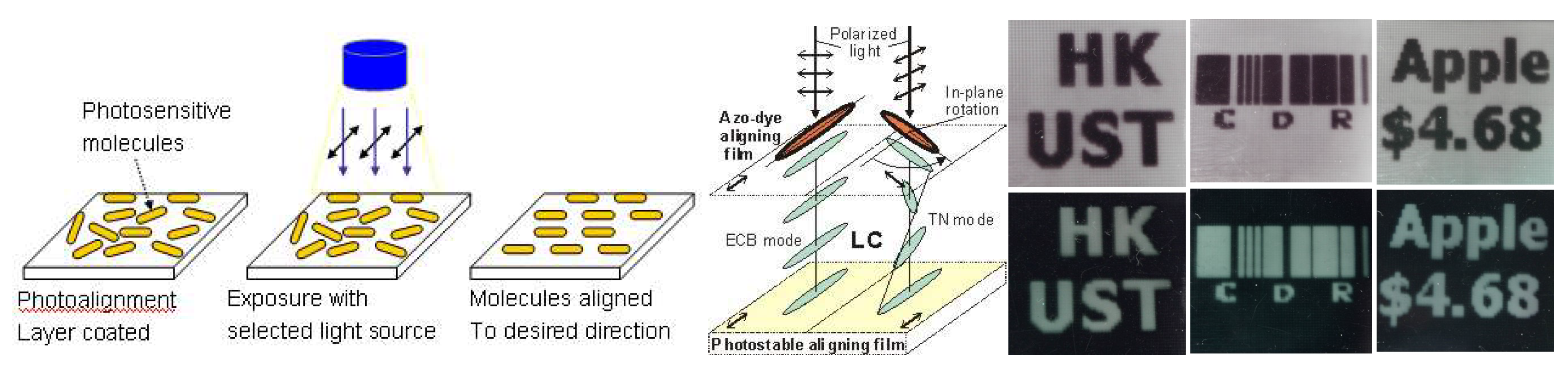
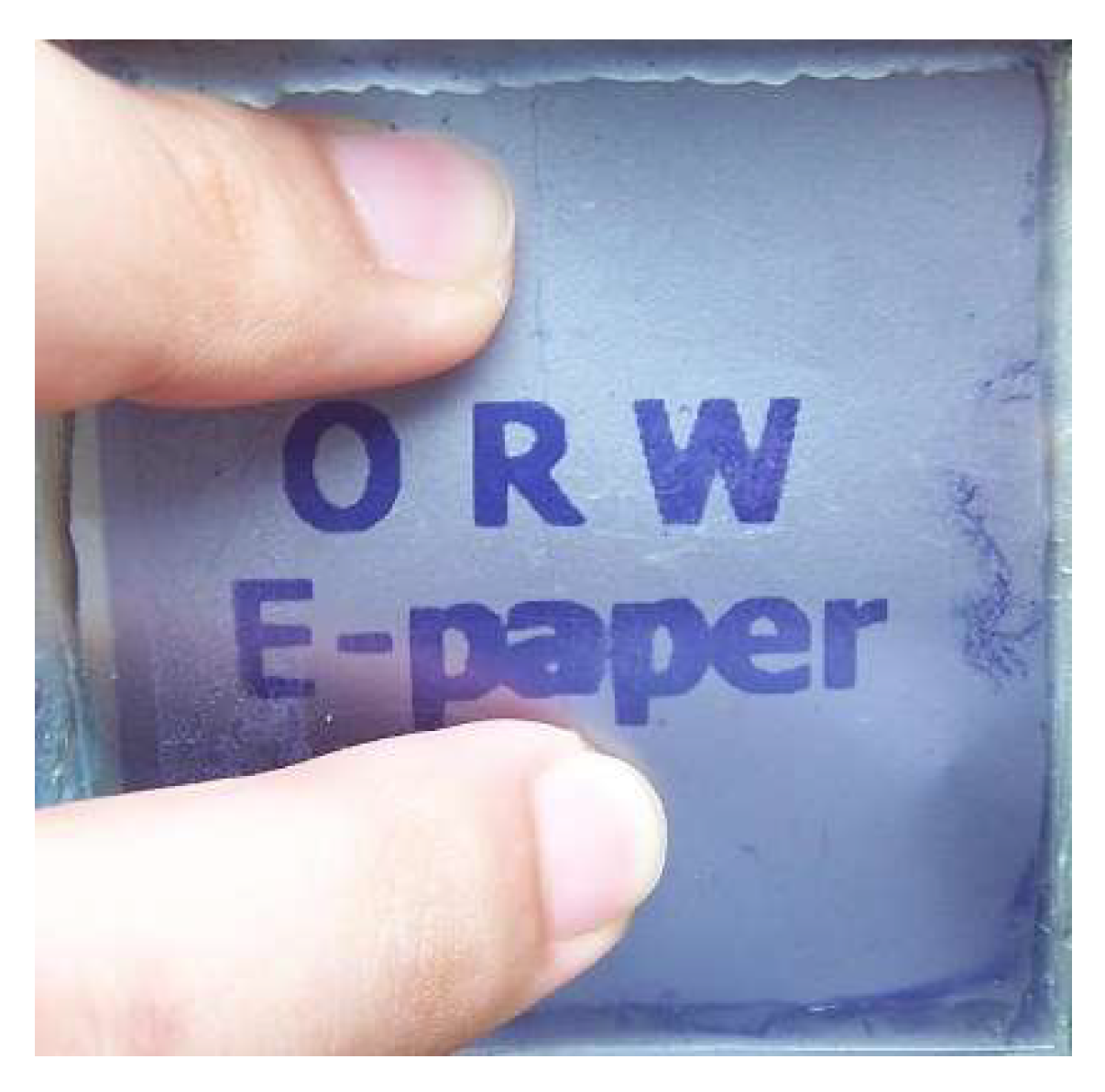
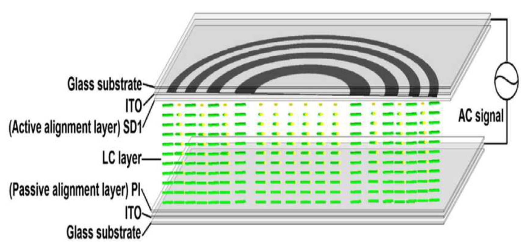
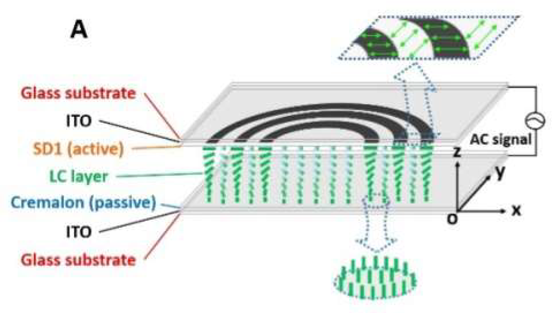
5]. Optical LC alignment can be considered as rewritable, and even though it suffers from complete image decay due to exposure under direct sunlight, the image can be easily restored or changed through a rewriting cycle via specific exposure devices. Photo-stability requirements of such optically rewriteable LC cell are notably diminished since the display unit does not undergo reversible changes. Optically rewritable technology is a modified method of azo-dye based photoalignment which possesses considerably high azimuthal anchoring energy and has a unique trait of reversible in-plane reorientation via photoalignment, i.e., photosensitive molecules tend to reorient perpendicular to the polarization of an incident light. Typically, an ORW LC cell comprises of two substrates with different alignment materials (
Figure 1).
One aligning material is optically passive and keeps its alignment direction on one substrate. The other aligning material is optically active and can change its alignment direction upon being exposed topolarized light through the substrate. In comparison with electrically controlled plastic displays, ORWs are significantly thinner, and do not require transparent conductive electrodes thus ITO photolithography and etching on a plastic substrate is not needed. By controlling the alignment direction of the photoaligning azo-dye layer, which is insoluble in the liquid crystal, switching and a continuous grey scale can be achieved. Hence, one can obtain the transmission level corresponding to the specified twist angle of LC in the ORW cell under the initial polarizer configuration. The tolerance of the cell gap variation of the ORW is very high, as no obvious change in LC transmission value is observed when the cell gap is changed by 50%, and achromatic switching of all grey levels in ORW can be obtained [
1,
2,
3,
4,
5]. Each of the transmission level is stable and the visualization of information on the ORW requires zero power consumption for a long time.
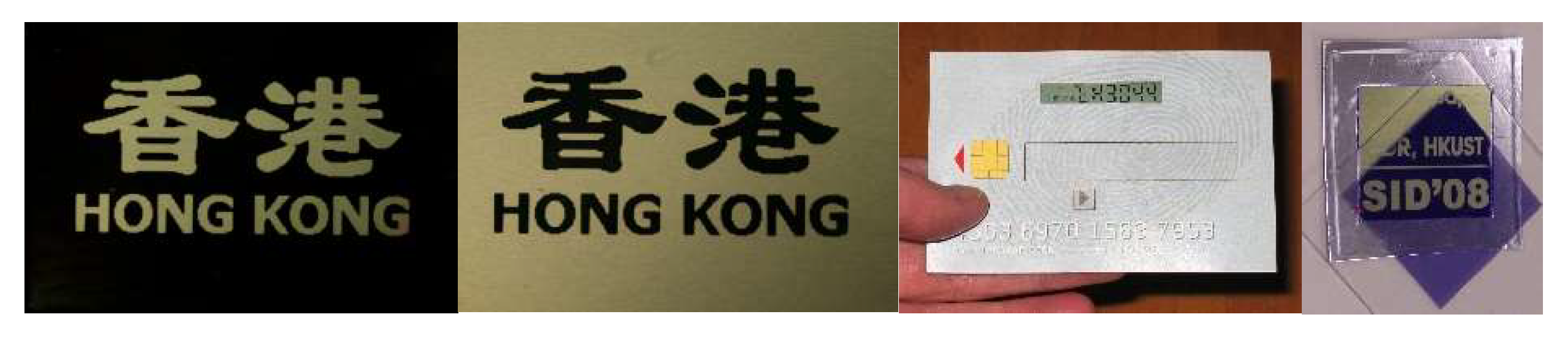
Due to the recent developments of ORW LCD and progress in LC photoalignment, it is possible to separate the E-paper display-unit and driving optoelectronics parts, and the resulting significant reduction of complexity of the ORW E-paper structure makes the properties and cost of both devices paper-like [
1,
2,
3,
4,
5]. Thus, ORW E-paper is very durable, economical and ready for the flexible challenge. More investigations on the operation of ORW have revealed that a cheap and low power consuming high-efficiency blue LED can be used as an alternative exposure light source, replacing expensive and high power-consuming mercury lamps or lasers. Aprototype of ORW E-paper with the device structure based on polarizer and plastic substrates was experimentally implemented [
6] (
Figure 2).
It operates by optically rewritable alignment technology, possesses grey scale capability, is truly stable, has no electrodes and does not require electric power to display an image with high contrast and wide viewing angles. Nowadays, a new function of the ORW E-paper on liquid crystal technology for displaying 3D images has been developed to enrich the performance of the single side light printable ORW E-paper which was conventionally designed for 2D images [
1,
2,
3,
4,
5,
6].
The light-sensitive photoaligning materials and liquid crystal layers were elaborated with regard to the following characteristics [
6]: optical writing/erasing time < 2 s, the energy of writing beam < 1 J/cm
2 with more than one thousand reversible cycles and implemented the blue LED as an exposure light source. Because of the insufficient durability of contact bonding and flexible conductor, E-paper displays encounter the issue of the high level of complexity of the driving electronics, therefore, optically rewritable technique is highly desirable.
The merits of ORW E-paper include no current conducting layer, no drivers, high tolerance of layer thickness, low manufacture cost (the price of the ORW E-paper is approximately equal to the price of two polarizers, i.e., about 20 USD/m
2). By using plastic substrates, the ORW E-paper as a pioneering innovation in LCD E-paper exhibits outstanding flexibility characteristics, and will easily find application in the E-paper market. Some possible applications of the ORW E-paper include light re-printable paper, labels, plastic card displays, 3D paper for security applications, etc. (
Figure 3).
3. Application of Photoalignment in Photonic LC Devices
LC photonic devices based on photoaligned materials, including passive elements for fiber optical communication used in fiber-to-the-home (FTTH)programs, are becoming increasingly important. FTTH is a form of fiber optical communication delivery where the fiber extends from a central location to the subscriber’s working or living space. Since the Gigabit and Terabit Ethernet can be efficiently used, fiber configurations that bring fiber right into the building can offer the highest speeds for delivering voice, video and data. Fast switching photo-aligned LC cells with microsecond and sub-microsecond switching time shall have the chance to replace the currently used micro-electro-mechanical (MEM) switching devices in FTTH systems with millisecond switching time [
7].
Reliable passive optical components are still in high demand, and their demand will continue to grow in the long run. Some LC components, such as LC-based polarization controllers, phase retarders and coaxial variable optical attenuators have already appeared on the market [
8,
9,
10]. Vescent Photonics (Golden, CO 80401USA) announced that LC waveguides could be a marvelous electro-optic technology platform for versatile applications, such as beam steerers, interferometers, lasers, tunable filters, etc. [
10].
Further investigations on the passive liquid crystal elements for the fiber optical communication systems is desirable. Silicon photonics-based devices (e.g., high-quality LC switches, voltage controllable filters and variable optical attenuators) as well as photoalignment LC technology-based devices (e.g., polarization rotators and controllers) have to be developed. New prototypes for packaging are highly desired. New LC materials for fiber optical communications that are working in the IR region have to be tested. LC tunable sensors including CMOS-based ones and LC lenses are becoming very important devices for LC photonics applications.
3.1. LC Switches
Switches for optical fiber networks are becoming more and more important. LC switches exhibit certain advantages as compared with the MEM switches that are commonly used for the same purpose, for instance: (i) fast switching time; (ii) low power consumption and controlling voltages; (iii) high reliability and durability [
7,
8]. Nevertheless, the characteristics of the thermal drift and the wavelength-dependent response time of LC switches should be avoided. We have investigated several LC electro-optical modes, which can be utilized for fabricating LC switches for optical fiber networks [
7,
8]:
- (1)
LC switches can make use of the effect of total internal reflection in nematic LC [
11,
12]. The total internal reflection switch operates only for TE mode, and the most promising approach is based on vertical aligned nematic (VAN) configuration, realized by photoalignment. The switching time of 1 ms can be easily obtained upon application of aswitching pulse amplitude of 5V [
12]. The quality of the total internal reflection switch strongly depends on the physical parameters of VAN as well as the boundary conditions including LC anchoring energy. The corresponding computer simulations show a good match with the experimental results [
12].
- (2)
A bypass optical switch that was based on two nematic LC cells with aswitching time < 200 μs was demonstrated by using two temperature-stabilized photoaligned nematic LC (NLC) cells [
13]. Two subsequent NLC cells with mutually orthogonal optical axes compensate the relaxation of NLC birefringence when they are turned off simultaneously. Thus the switching time of the two-cell switch can be as short as the turn-on times of the NLC cell. The NLC cells can be designed for a certain fiber wavelength by adjusting the cell gap thickness. However, the drawback of the system is the necessity of the synchronous relaxation of the two cells, which may take several milliseconds.
- (3)
An LC switch can be designed to control the light propagation in the plane of LC layers [
14]. It was experimentally demonstrated that the propagation of the light beam can be noticeably changed by refraction and reflection of light at the sharp boundaries between the regions with different LC orientations induced by photoalignment [
14]. LC switches can be electrically controlled. Certain methods were proposed for optimizing the insertion loss and crosstalk of the 1 × 2 switch for practical photonic applications. It is possible to create N × M switch and various optical processing data elements (e.g., attenuators) by using different photoalignment templates. There are many ways to optimize such types of LC devices, and employing fast operating ferroelectric liquid crystal layers is one of those possible ways, which can provide the microsecond-level operation time.
3.2. Polarization Controllers and Polarization Rotators, Variable Optical Attenuators
Polarization controllers are optical elements that can convert an arbitrary input state of polarization (SOP) to the desired one, thus governing the unpredictable polarization change that stems from the polarization-dependent components of the optical fiber system. These optical elements can be made of three successively placed LC cells, which utilize the electrically controlled birefringence (ECB) to modify the evolution of the SOP [
15]. The switching times typically depend on the LC material and are of the order of 10 ms for a wavelength of 1.3 μm [
15].
A polarization rotator is an optical element that can rotate the linear polarization of the input light to any desired polarization plane [
5]. The configuration of our proposed LC polarization rotator comprises of a polarizer and two LC homogeneous cells placed with their optical axes making 45° with respect to each other. One of the LC cell provides a voltage controllable phase change, and the other is fixed as a quarter wave plate [
5]. Such an optical element can rotate the light polarization state at any angle between 0° and 90° dependent on voltage.
LC variable optical attenuators (VOA) typically have attenuation ranges of 30 dB for an applied voltage of 12 V in the wavelength range of 1525–1575 nm [
7] with a response time of ~10–30 ms. Some of them are basically dependent on the light scattering of a polymer network (PN)-filled LC (PN-LC) cell. As a result of the refractive index mismatching of the polymer and LC in absence of the driving voltage, the light from the input fiber was scattered, and it could mostly pass through the PN-LC layer due to the refractive index match of the polymer and the LC in presence of the applied voltage.
3.3. LC Filled Photonic Crystal Fiber
Photonic crystal fiber (PCF) is a polymer or glass fiber with an array of tiny air holes running along the length of the fiber. The waveguide properties of such fibers can be controlled by filling an additional material into the air holes [
7,
16,
17,
18,
19]. The refractive index of the LC can be easily tuned by modifying the electric field or temperature, therefore LCs are suitable for this purpose. The technique of light reconfigurable alignment of LC in glass micro-tubes and in PCF was developed (
Figure 4) [
7,
16,
17,
18,
19].
Fairly homogeneous alignment was verified by polarizing optical microscope and FTIR spectroscopy methods. Based on proper developed photoaligning azo-dye materials [
20], the presented alignment technique is a promising non-contact method for LC orientation in complicated photonic crystal structures. The order parameter (S) of LC has been acquired from FTIR spectroscopy data and the good alignment quality was proved. Moreover, LC filled thin porous films will be also investigated, for the purpose of practical applications in electrically controlled optical attenuators and polarization-insensitive optical switches [
21].
3.4. Switchable Diffraction Grating
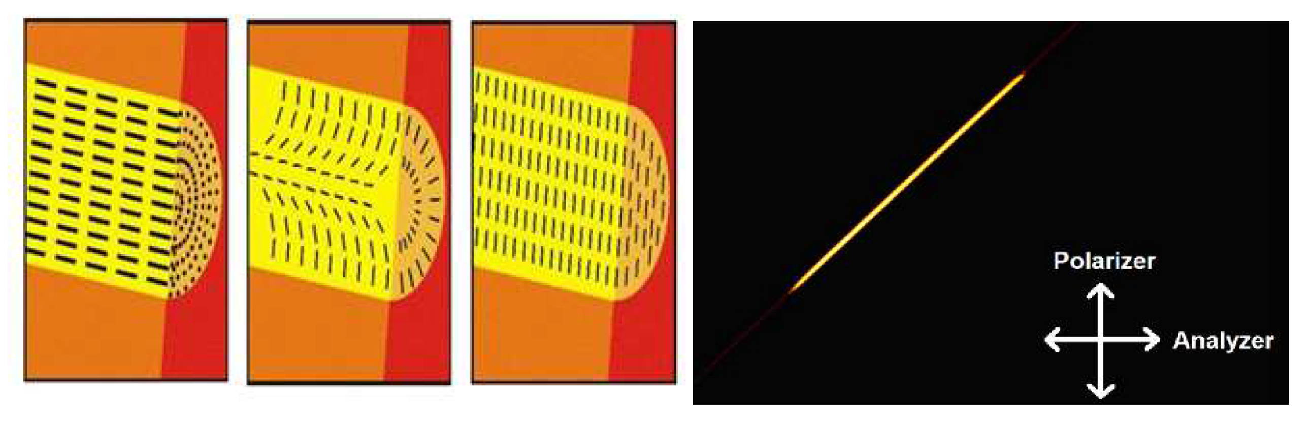
Remnant high-efficiency polarization gratings were fabricated in nematic liquid crystal cells by exposing the layers of azo-dye molecules deposited on the substrate to “interfering” beams with opposite circular polarizations [
22]. The diffraction pattern was controlled by an electric signal applied across the LC cell. The polarization gratings are suitable for electrically controlled detection and discrimination of polarized components of light. All LC molecules tend to be reoriented to a uniform homeotropic state at high voltage, and the modulation of LC alignment in the cell is terminated. Applications in LC optical switches are discussed.
A diffraction grating was proposed by periodically defining the liquid-crystal director distribution to form alternating planar aligned (PA) and twist nematic (TN) regions in an LC cell sandwiched between two crossed polarizers [
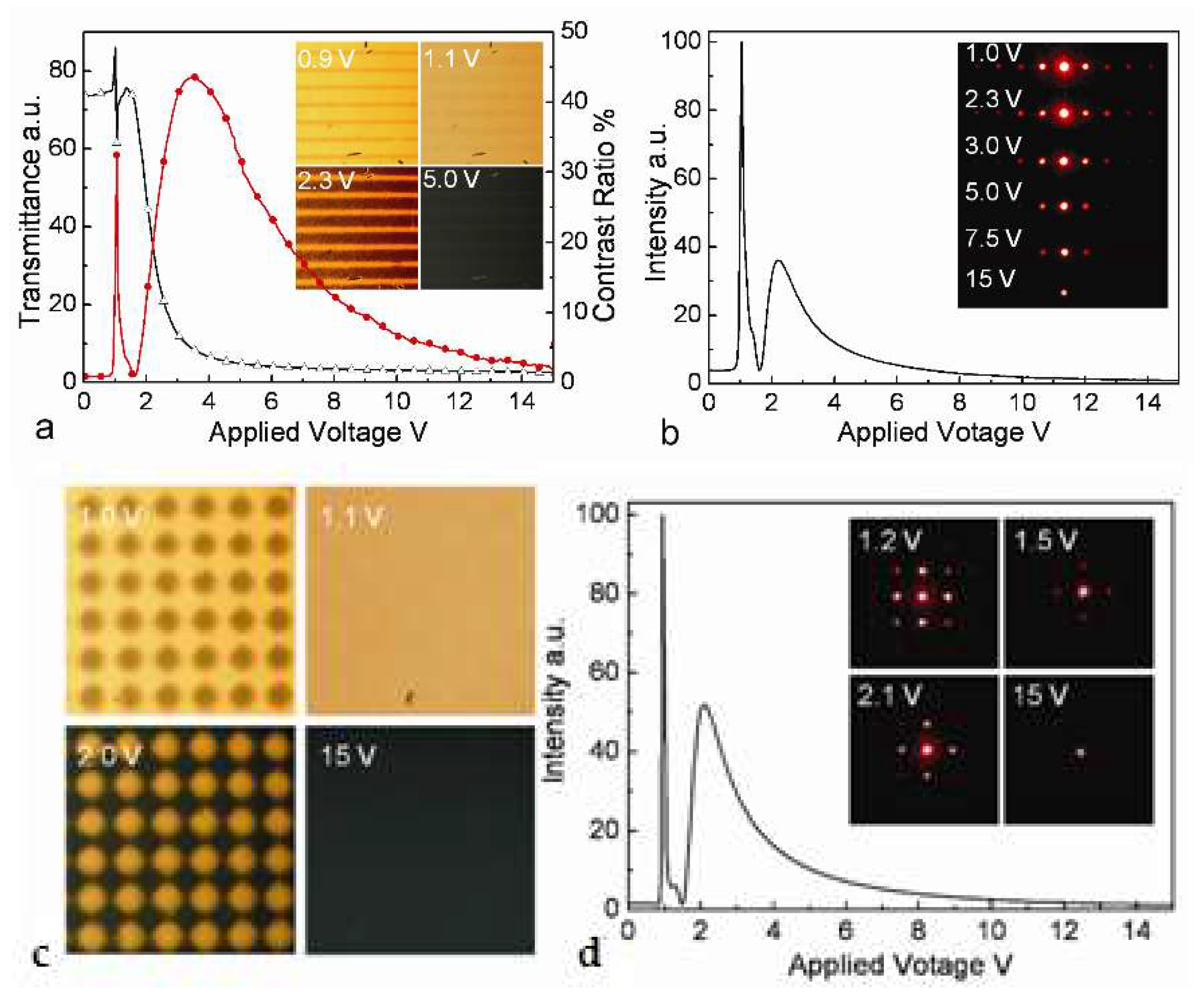
23]. Both 1D and 2D diffraction gratings are demonstrated with diffraction efficiency of total 1st order up to 12.0% and 18.2% respectively (
Figure 5), due to their different voltage-dependent transmittance and phase modulation. When a voltage was applied, four characteristic states were achieved and the intensity of 1st order could be suppressed by approximately 2 orders within 0.3 Vp-p at driving voltage < 2.5 Vp-p.
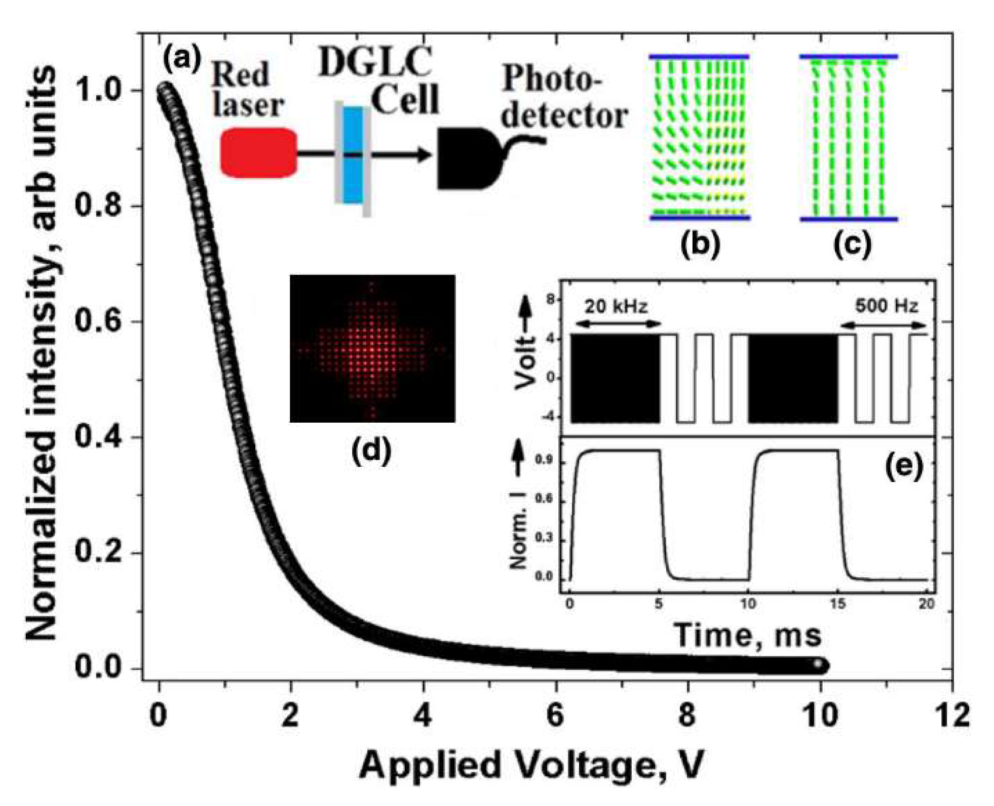
A Dammann grating based on the hybrid photo-aligned dual-frequency nematic liquid crystals was demonstrated [
24]. The configuration of the Dammann grating is comprised of two substrates, one of which is coated with the homeotropic alignment, and the other substrate provides a planar, patterned alignment with a mutually orthogonal easy axis in every two adjacent alignment domains. The fabricated polarization independent Dammann grating generated an optical array with equal light intensity distribution, which was characterized by a low uniformity deviation of ~0.081, a diffraction efficiency of more than 58%, a response time < 1 ms, and a low driving voltage of ~3 V/μm (see
Figure 6).
3.5. Optically Rewritable Technology for Photonics Devices
Optical rewritable technology (ORW) pioneered by us [
3,
4,
5] can be successfully used for photonics applications. LC materials with optimized electro-optical properties provide a promising opportunity for application devices. As we know, there are no publications published by other groups on the application of optically rewritable technology for LC photonics devices. Several key devices are developed, for examples, light controllable LC plane waveguides, LC polarization dependent elements, lenses and wave plates, LC polarization rotators and polarization controllers, light and voltage controllable diffraction gratings for optical filters etc. One of such applications is shown in
Figure 7.
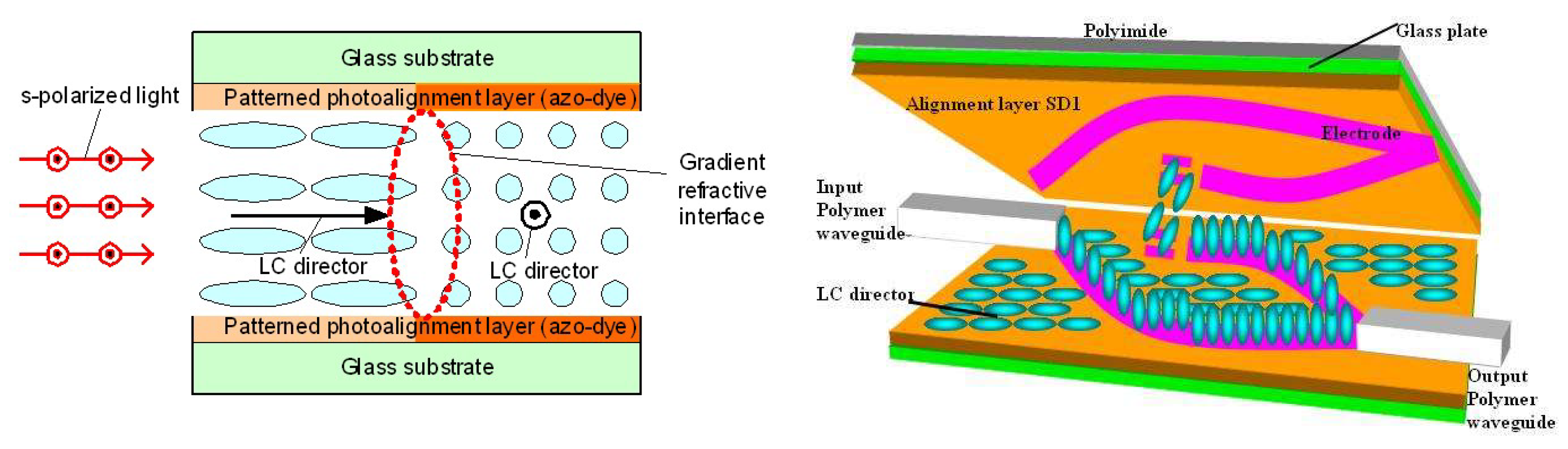
Using ORW photoalignment techniques the smooth collimating refractive interface can be written by light in front of the waveguide immerged into LC (
Figure 6) [
25]. The LC structure can be stabilized by the photoalignment layer without operation of applied voltage. S-polarized light can be coupled and comes from the waveguide, going into a collimated beam inside LC bulk for further processing, while the p-polarized light can be guided by matching polarization maintaining LC waveguide [
25]. We developed the polarization independent design of the LC photonic device that can convert both polarization components out-coupled from polarization independent waveguide to one polarization for further processing of light by the polarization-dependent LC structure for routing or other purposes. This new design consists of polarization maintaining LC waveguides, LC polarization dependent passive lens and active half wave plate (HWP) [
25].
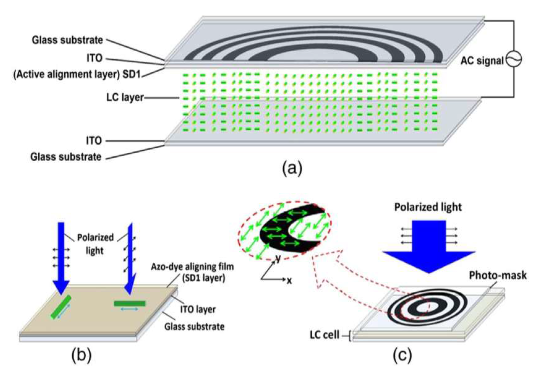
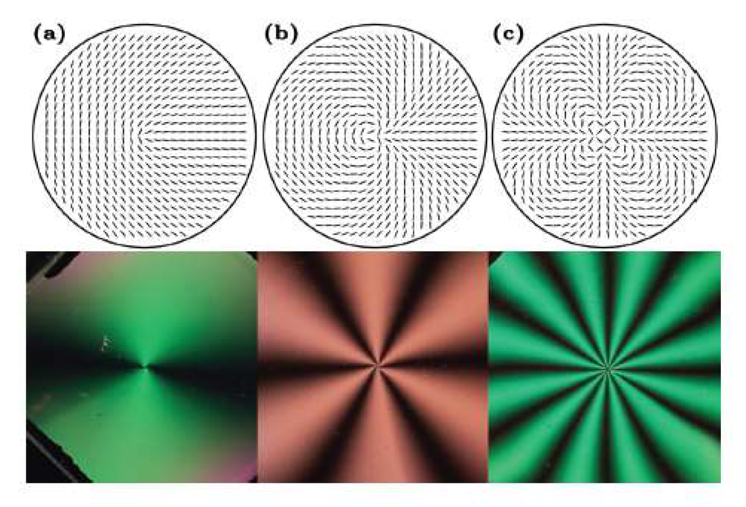
Based on the outstanding ORW properties of the photoalignment material, a binary-phase liquid crystal circular Dammann gratings with two mutually orthogonal light-induced alignments in neighboring alignment domains was proposed to generate annular patterns with equal-intensity distribution in the far field [
26]. A simple mask-free real-time optical tuning of the liquid crystal circular Dammann grating was achieved by merely controlling the polarization of an ultraviolet exposure light as well as the energy dose, as shown in
Figure 8. The proposed liquid crystal circular Dammann gratings with high efficiencies and desirable uniformities exhibited outstanding optical and electrical tunabilities.
3.6. Patterned Micro-Polarizer Array Using Photo-Alignment Technology for Image Sensor
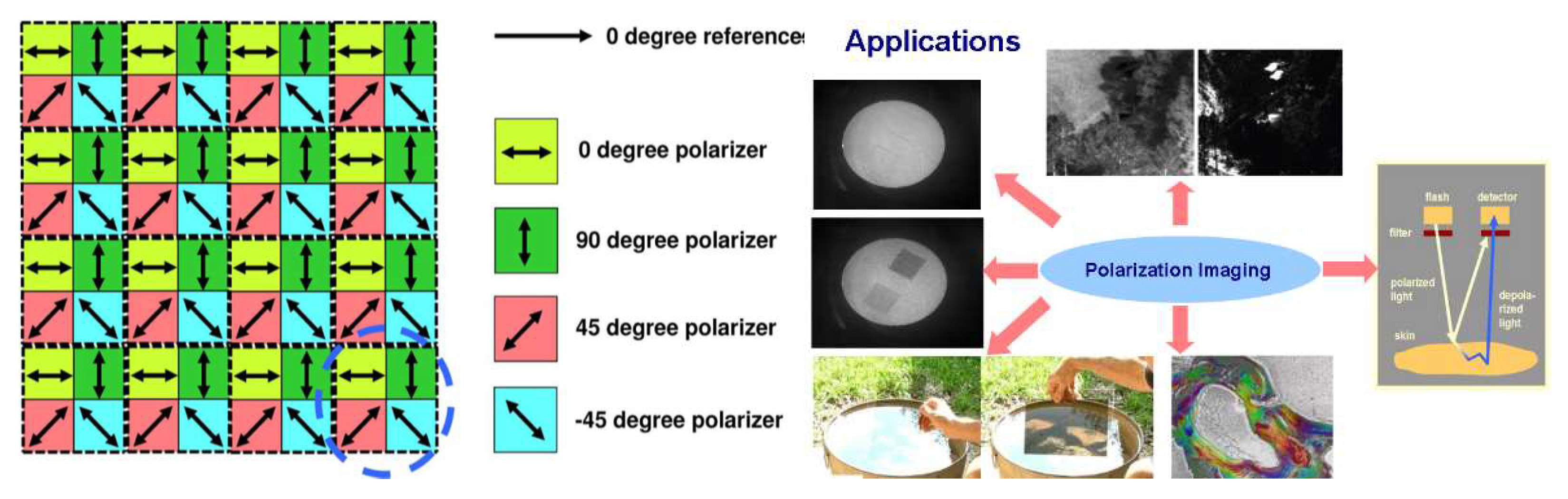
A thin patterned micro-polarizer array which is generated by photo-alignment method for complementary metal–oxide–semiconductor (CMOS) image sensors can be made for a simultaneous detection of all four Stokes parameters of an output optical image (
Figure 9) [
27,
28,
29,
30]. A 2 μm pitch can be achieved by using UV light to rotate the four micro-polarizer elements. The experimental results prove the concept of high-performance photo-aligned LC micro-polarizer arrays with a high transmittance of ~80% and extinction ratio as high as ~3200 (35 db).
A high transmittance and extinction ratio micro-polarizer array technology exploiting “guest-host” liquid crystals mode for visible imaging polarimetry has been developed [
30]. This high resolution thin micro-polarizer arrays with a 5 μ × 5 μ pixel pitch and a thickness of 0.95 μ achieved by the “host” nematic liquid crystal molecules photo-aligned of sulfonic azo-dye SD1. The averaged major principal transmittance, polarization efficiency and order parameter are 80.3%, 86.3% and 84.8% respectively, across the 400–700 nm visible spectrum range. The proposed fabrication technology completely removes the need for any selective etching during the fabrication/integration process of the micro-polarizer array. It is fully CMOS compatible, and is simple and cost-effective, requiring only spin-coating followed by a single ultraviolet-exposure through a “photo-alignment master”. It is well suited for low cost polarization imaging applications.
3.7. Electrically Tunable Liquid Crystal q-Plates
A photo-alignment technology is used to fabricate liquid crystal q-plates tuned by electricity with various topological charges for generating optical vortex beams with definite orbital angular momentum (OAM) per photon [
31,
32]. Several tests are made on the q-plates, including OAM tomography, showing excellent optical performances. These devices can have useful applications in general and quantum optics. The azo-dye materials showed a very high-resolution capability of LC alignment in these experiments (
Figure 10).
3.8. Electrically Switchable Liquid Crystal Fresnel Lens
A liquid crystal Fresnel lens based on alternate twisted nematic (TN) and planar aligned (PA) regions (see
Figure 11), was fabricated by means of a two-step photo-alignment process [
33]. The liquid crystal Fresnel lens manifested two identical focal lengths on account of the TN and PA alignment domains, giving rise to the double light intensity at the focal point, and thus offered double efficiency of the conventional Fresnel zone plates.
A method of fabricating a liquid crystal Fresnel lens based on single alignment layer with patterned planar-aligned regions was disclosed by Wang et al. [
34] The binary-phase liquid crystal Fresnel lens manifested a diffraction efficiency of 39% at the focal point. Due to the mutually orthogonal alignment in neighboring domains (see
Figure 12), the fabricated Fresnel lens possessed a polarization-independent property, which was indeed a merit in the viewpoint of efficient use of energy.
A polarization independent Fresnel lens based on a patterned hybrid aligned nematic dual-frequency liquid crystal was demonstrated [
35]. The liquid crystal Fresnel lens was fabricated by assembling two glass substrates with different alignment materials. One substrate was coated with a homeotropic alignment layer and the other one was coated with an in-plane patterned alignment layer, wherein the easy axes in every two adjacent alignment domains were mutually orthogonal, as shown in
Figure 13. Due to the outstanding electro-optical properties of dual frequency liquid crystal, the proposed Fresnel lens exhibited fast switching time under alternate high frequency and low frequency electric fields.
3.9. Liquid Crystal Optical Elements with Integrated Pancharatnam-Berry Phases
A polarization-dependent diffractive bifocal vortex lens based on the Pancharatnam-Berry phase was experimentally demonstrated [
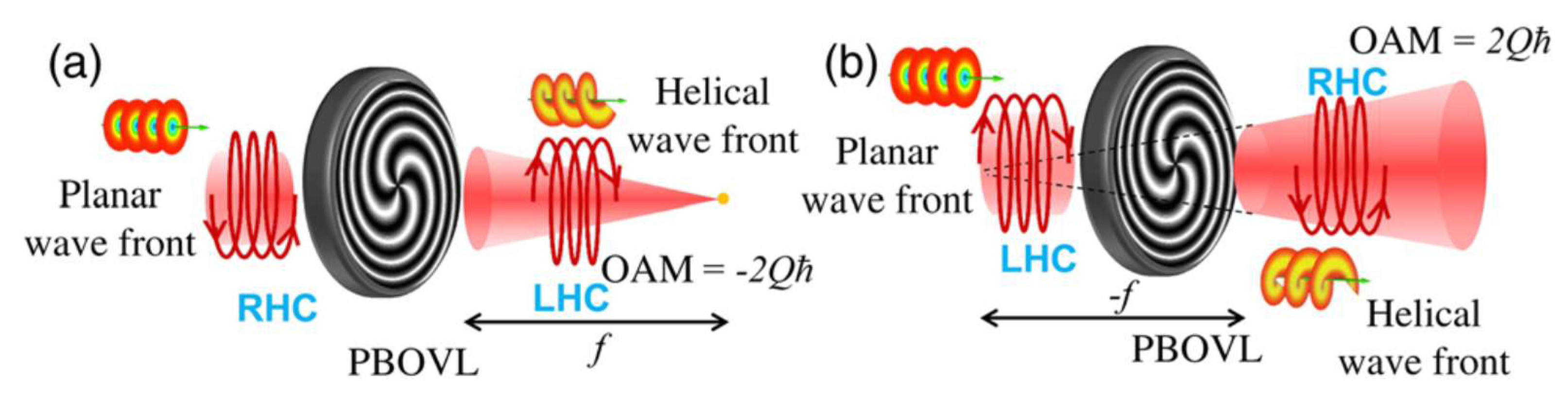
36]. The phase expression of the Pancharatnam-Berry-phase optical-vortex lens (PBOVL) comprised of two terms, i.e., a Pancharatnam-Berry lens term and a q-plate term. Non-separable spin angular-momentum (SAM) and orbital angular-momentum (OAM) photon states were established when an incident beam passed through the PBOVL, as shown in
Figure 14. Different OAM states at the output of the PBOVL could be sorted by the bifocality of the fabricated lens. By using the underlying physics of the Pancharatnam-Berry-phase polarization holography, the device was facilely, efficiently, and economically realized. The transmittance and diffraction efficiency of the fabricated device were measured to be 90% and 91%, respectively.
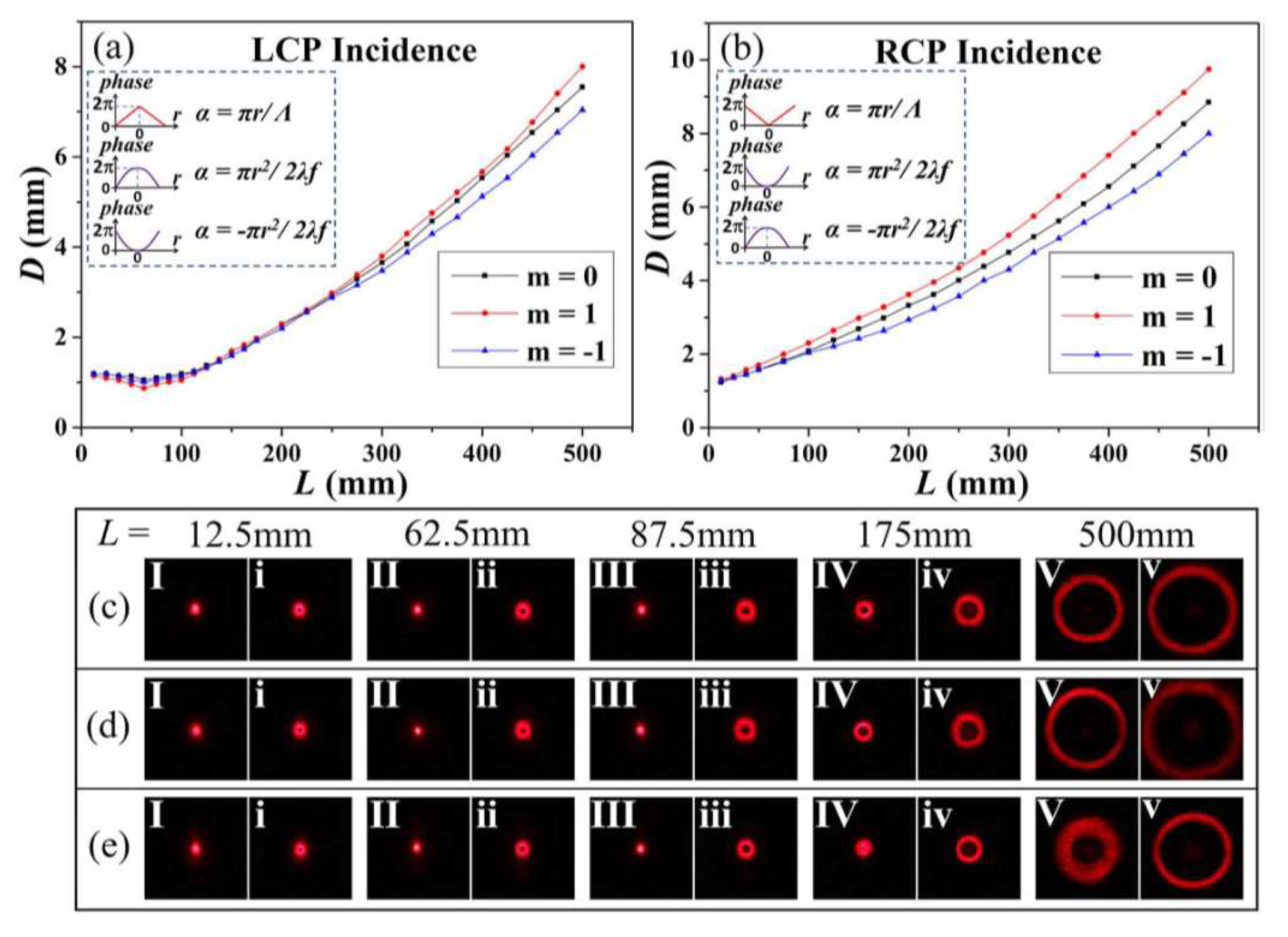
A liquid crystal Pancharatnam–Berry (PB) axilens was fabricated via a digital micro-mirror-device (DMD)-based photo-patterning system [
37]. The polarization-dependent device behaved as an anti-axilens for a RHC polarized incident light, for which an optical ring gradually expanded in the transverse direction at the output, and it acted as an axilens for an LHC polarized incident light, for which an optical ring was focused with a long focal depth at the output. The modification of the size and the sharpness of the diffracted hollow beam was demonstrated by encoding a positive (negative) PB lens term into the director orientation expression of a PB (anti-)axicon, as shown in
Figure 15.
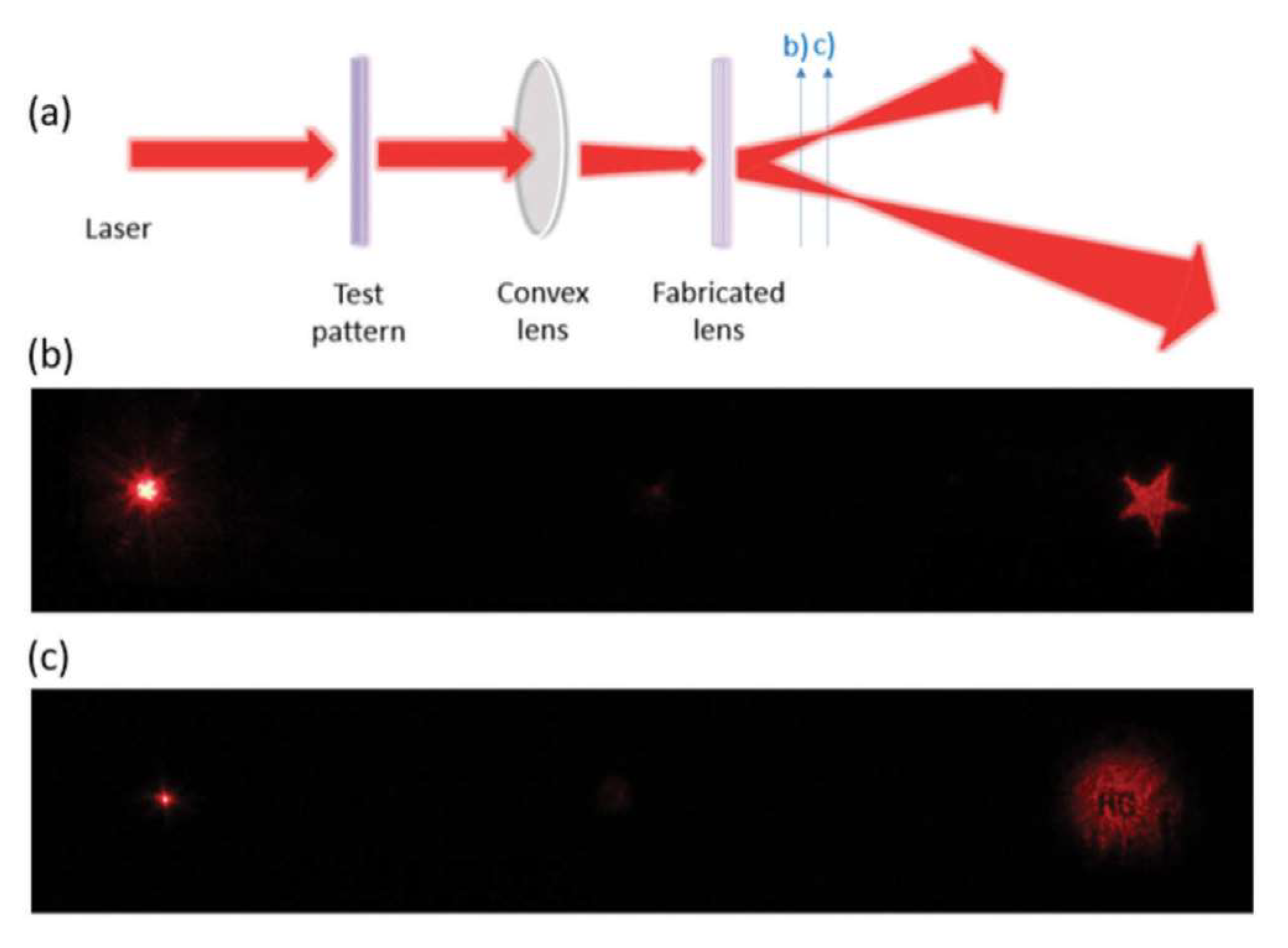
A liquid crystal beam splitting lens with spatially separated focuses via liquid crystal photoalignment technology was fabricated [
38]. The proposed lens with exotic optical properties was realized by integrating a polarization grating with a Pancharatnam-Berry phase LC lens. The two focuses of the proposed lens, i.e., +f and −f, could be spatially separated (see
Figure 16). When a linearly polarized incident light successively passed through a conventional convex glass lens with a proper focal length and the fabricated lens, the two emergent light beams exhibited convergent optical behavior and the two focuses were spatially separated. Moreover, by adjusting the distance between the proposed lens and the conventional glass lens, the focal lengths of the lens system could be modulated.
4. Conclusions
Liquid crystal (LC) photoalignment and photopatterning technology for new display and photonics applications is a hot research area. Such elements have started to appear in displays and the photonics market. The electro-optical modes used for the purpose including the light polarization rotation, voltage controllable diffraction and fast switching of the LC refractive index. Photo-alignment techniques make it possible to develop new LC fiber components. Photo-aligning materials are used to align LCs in super thin photonic holes, curved and 3D surfaces and as cladding layers in micro-ring silicon based resonators. The prototypes of new LC efficient photonics devices, such as optically rewritable LC E-paper and waveguides and voltage controllable diffraction gratings are envisaged. The polarization controllers, polarization rotators, variable optical attenuators and other passive LC optical elements for fiber communication networks are under way. We hope this review will be interesting for not only to a wide range of engineers, scientists and managers, who are willing to develop new LC displays or other LC photonics devices and optical components, but also to the researchers in other practically important fields, where the formation of new highly ordered structures of the organic molecules is highly desirable.


