Abstract
The motivation to search for signatures of superconductivity in Weyl semi-metals and other topological phases lies in their potential for hosting exotic phenomena such as nonzero-momentum pairing or the Majorana fermion, a viable candidate for the ultimate realization of a scalable quantum computer. Until now, however, all known reports of superconductivity in type-I Weyl semi-metals have arisen through surface contact with a sharp tip, focused ion-beam surface treatment or the application of high pressures. Here, we demonstrate the observation of superconductivity in single crystals, even an as-grown crystal, of the Weyl semi-metal tantalum phosphide (TaP), at ambient pressure. A superconducting transition temperature, , varying between 1.7 and 5.3 K, is observed in different samples, both as-grown and microscopic samples processed with focused ion beam (FIB) etching. Our data show that the superconductivity present in the as-grown crystal is inhomogeneous yet three-dimensional. For samples fabricated with FIB, we observe, in addition to the three-dimensional superconductivity, a second superconducting phase that resides on the sample surface. Through measurements of the characteristic fields as a function of temperature and angle, we are able to confirm the dimensionality of the two distinct superconducting phases.
1. Introduction
Since the discovery of Weyl semimetals, a great deal of work has been devoted to understanding the properties of these topological materials, whose band structure includes specific points known as Weyl nodes where non-degenerate bands touch each other and disperse linearly. Weyl semimetals differ from the related Dirac semimetals in that they require either time-reversal or inversion symmetry to be broken in order to lift the degeneracy of the nodes. Consequently, Weyl nodes always exist in pairs of opposite chirality that are connected through Fermi arcs running along the surface of the material, as has been observed experimentally in several materials using angle-resolved photoemission spectroscopy (ARPES) [1,2,3,4,5,6,7]. The chiral nature of the Weyl nodes can furthermore manifest itself in electrical transport, in the form of the chiral anomaly, leading to a negative longitudinal magnetoresistance. The observation of this effect has been reported in several materials [8,9,10,11,12], but its origin remains uncertain [13,14,15].
In addition to the intrinsic transport properties of Weyl semimetals, the combination of Weyl physics and superconductivity may support Majorana [16] or other exotic surface states [17] as a result of their topological nature. These states are of fundamental interest, as ultimately, they may be applicable in the field of quantum computation. For this reason, there is an ongoing effort aimed at achieving superconductivity in such materials and investigating their properties, either through the use of the proximity effect [16,18] or by other means. Successes in this area have been achieved for the type-II Weyl semimetals MoTeS [19] and TaIrTe [20], which exhibit intrinsic, exotic superconductivity. For type-I Weyl semimetals, however, such observations are still lacking.
The family of compounds comprising TaP, TaAs, NbAs and NbP are all experimentally confirmed as type-I Weyl semimetals [2,3,5,21,22,23] and are now among the most ardently studied compounds in this class. Under the right conditions, each member of the family has shown trace signatures of superconductivity. In both TaAs and TaP, a superconducting onset has been induced through contact with sharp tips of different materials [24,25,26,27], while in TaP alone, this onset was also achieved under the application of extremely high pressures [28]. In the former case, however, the specific technique does not allow for the observation of zero resistance, while in the latter, only a partial drop in the resistivity was observed. Similarly, signs of partial superconductivity were also seen in polycrystalline [29] or powder [30] samples of NbP. A state of zero resistance, however, has only been reported in samples where superconductivity was induced in a thin surface layer by treatment with focused ion beam (FIB) [31]. To date, no trace of superconductivity at ambient pressure has been reported in pristine single crystals of any member of this family.
In this work, we demonstrate the onset of intrinsic three-dimensional superconductivity in TaP, in addition to the FIB-induced surface superconductivity that was previously reported by Bachmann et al. [31]. In one of our FIB-processed crystals, both two- and three-dimensional superconductivity are observed, while in the as-grown parent crystal only three-dimensional but inhomogeneous (filamentary) superconductivity appears. In both cases, we find to vary between 1.7 and 5.3 K. Finally, we delineate and identify the two transitions in the microfabricated crystal based on the angle dependence of its characteristic magnetic fields. The presence of three-dimensional superconductivity in the microfabricated crystal, as revealed through this analysis, confirms that superconductivity develops within the bulk of the as-grown crystal. Though its origin could not be confirmed in this initial study, we speculate here that it may arise from domains within the crystal with excess Ta.
2. Results
Figure 1b shows low-temperature resistivity curves for both the pristine crystal and one of the microstructured samples, labelled sample 4 (data for all four microstructured samples can be found in Figure S1 of the Supplementary Information). The parent crystal exhibits an incomplete, resistive transition at a transition temperature = 3 ± 0.8 K that resembles the one which had been observed previously in TaP under high pressure [28]. The microstructured crystal, by contrast, exhibits a sharp transition to zero resistance with = 3.3 ± 0.5 K. Note that the other microstructured crystals showed either broad and/or incomplete transitions. As a consequence, we focussed our subsequent measurements and analysis on sample 4.
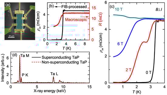
Figure 1.
(a) False color SEM image of a typical FIB contacted crystal. (b) Temperature sweeps showing the resistive transition of the FIB-processed sample 4 and the macroscopic crystal from which all FIB samples were cut. (c) Resistivity curves at low temperature of FIB-processed sample 4, under different, constant magnetic fields perpendicular to the current direction. (d) EDX spectra of the bulk sample used in our experiments and a non-superconducting sample obtained from a different source. Within the resolution, the compositions are the same.
In order to confirm the presence of superconductivity in our samples, we studied the evolution of the resistive transition in the presence of a magnetic field. Figure 1c shows temperature sweeps of the resistivity of one of the microstructured samples under different, constant magnetic fields, applied perpendicular to the current direction. Clearly, the resistive transition in the FIB-processed sample is suppressed gradually with field, as is expected in the case of a superconducting transition. For = 10 T, it vanishes completely. In the parent crystal, the transition is suppressed more strongly and vanishes under a very small magnetic field.
Superconductivity has been reported before in microfabricated samples of TaP, TaAs, NbP and NbAs [31], but in as-grown TaP it has never been observed at ambient pressure despite the large number of measurements at low temperature that have been carried out on this material [32,33,34,35]. For this reason, we investigated our bulk crystal for any deviations in terms of composition and structure that might indicate the origin of the superconductivity.
We studied the parent crystal with EDX and compared the stoichiometry with that of a non-superconducting crystal of TaP from a different source. The resulting spectra are shown in Figure 1d. From these spectra, we find that the two crystals have a stoichiometry that is identical to within an experimental error of about 1%, implying that our material has a very similar composition to that used in other studies. Furthermore, XRD measurements (see Supplementary Information, Figure S8) confirm that our TaP crystal is in the space group, as is usual for TaP under ambient conditions [21,36,37]. This structure is different, however, to that found in TaP under high pressure or in MoP (also under pressure), where in both cases, superconductivity appears in the P- phase. Thus the superconducting state that develops in our crystals appears to be distinct from what has been observed before.
Figure 2a shows field sweeps of the resistivity of one of the microstructured crystals (sample 4) under different orientations of the magnetic field. Here, the angle 90° denotes a field parallel to the direction of the applied current (see inset of Figure 2b), which in this case is the crystallographic -plane. For angles away from 90°, there is a clear double transition that we associate with distinct superconducting phases. Close to 90°, the characteristic fields of the two superconducting phases appear to merge, causing the two transitions to become indistinguishable.
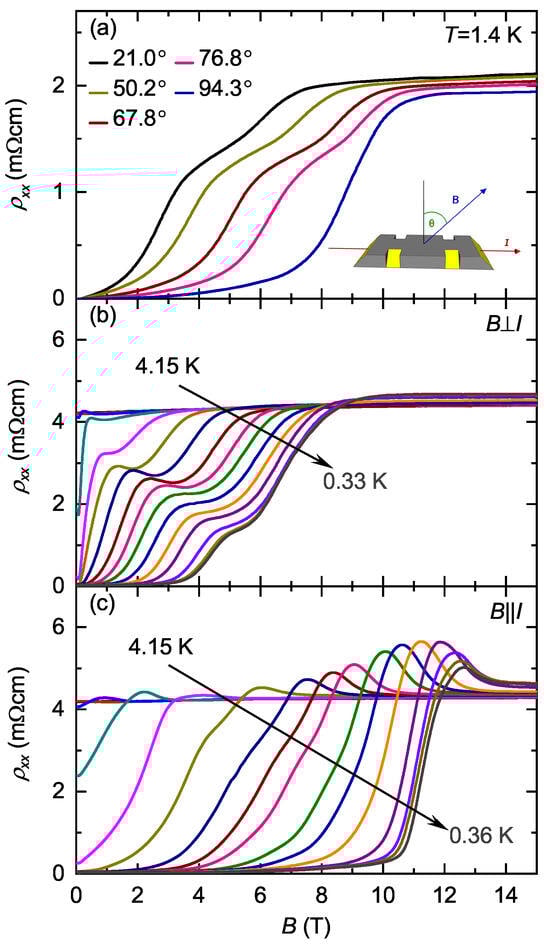
Figure 2.
Field sweeps of the resistivity of the FIB-processed sample 4 for (a) different angles as defined in the inset and (b) different temperatures in a magnetic field parallel to the current direction and (c) in a field perpendicular to the current.
Figure 2b,c show the temperature dependence of the resistive transitions in field, for fields perpendicular and parallel to the current direction, respectively. In perpendicular field (Figure 2b), there are two distinct superconducting features separated by a broad shoulder. In the parallel field configuration on the other hand, the shoulder is much weaker. This suggests that the characteristic fields of the two states are of similar magnitude, but have a different temperature dependence. The data also reveal an upturn in the resistivity before the normal state is fully restored. Such an upturn is frequently observed in inhomogeneous superconductors [38,39,40,41,42] due to current redistribution as some parts of the crystal turn superconducting while others remain resistive [43]. It was also recently seen in the pressure-induced superconducting state of MoP [44].
3. Discussion
3.1. Dimensionality of the Superconducting Phases
The data in Figure 2 can be used to extract characteristic fields for both transitions as a function of angle and temperature, the results of which are shown in Figure 3. The two field scales are determined by defining the field at which the resistance has risen to 90% of the normal state () and the field that minimizes the second derivative of the resistivity () (see Supplementary Figure S2 for more detail). In Figure 3a, we show both and as a function of the angle between the magnetic field and the c-axis. The solid and dashed lines are fits to the two-dimensional Tinkham model [45] and the three-dimensional Ginzburg–Landau (GL) model [46], respectively. It is found that the 2D Tinkham model gives an excellent description of the behavior of , covering not only the cusp at 90° that the 3D GL model misses, but also its behavior in near perpendicular fields. Conversely, the angle dependence of does not have a sharp cusp like and is better described by the 3D GL model.
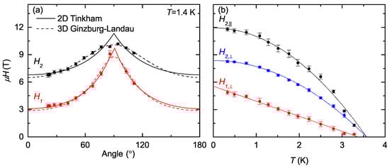
Figure 3.
(a) Angle dependence of the characteristic fields, fitted with the two-dimensional Tinkham model (solid lines) and the three-dimensional Ginzburg–Landau model (dashed lines). (b) Temperature dependence of the characteristic fields for parallel and perpendicular fields. is fitted using a three-dimensional model and with the two-dimensional Ginzburg–Landau model. in a parallel field cannot be unambiguously identified and is thus omitted from this figure.
Some refinements of the 2D Tinkham model are possible (outlined in the Supplementary Information), one for the case of intrinsic surface superconductivity and another for a thin superconducting film with a thickness less than or comparable to the coherence length , a less stringent requirement than that of the Tinkham model which requires a thickness [47,48]. Both of these adapted models, however, lead to a less accurate fitting for both and (see Supplementary Figure S3). Thus, with the GL and Tinkham models giving the most accurate descriptions of and respectively, we conclude that arises from a certain superconducting volume fraction within the interior of the crystal while is characteristic of a 2D superconducting state, presumably arising from a very thin layer on the surface that satisfies the criterion of .
Figure 3b shows the phase diagram of FIB-processed TaP, in both parallel and perpendicular field configurations. is only shown for perpendicular field, as it is not distinguishable in the parallel field configuration. The behavior of in both configurations can be well described by the expression , in agreement with the description of the critical field for a three-dimensional GL superconductor. on the other hand, is better described with a linear temperature dependence, consistent with the GL model for two-dimensional superconductors: [49,50,51]. Associating with the upper critical field for the two-dimensional superconducting layer, we can estimate to be approximately 7.7 nm.
The origin of the 2D superconductivity is believed to be the presence of excess Ta induced during FIB milling. In order to make an estimate of the thickness d of the superconducting layer, we use the SRIM-2013 [52] code to simulate the ion milling process. With the low acceleration voltage of 8 kV that is used for the final polishing of the sample, the Ga ions penetrate about 5.0 nm below the surface of the sample. As P is sputtered approximately two times more readily than Ta, an average composition is expected in this thin layer of TaP. Of course, the thickness of the superconducting layer cannot simply be assumed to be the same as the ion penetration depth; if anything, this depth gives an upper limit. Considering this, it is not unreasonable to expect that the inequality is indeed satisfied.
3.2. Critical Currents
Information on the evolution of the two superconducting phases in sample 4 with temperature can be gleaned by looking at the critical currents associated with the transitions. To this end, we measured the current-voltage (IV) characteristics and differential resistivity curves in different magnetic fields and temperatures. In Figure 4, the data are shown for zero field at T = 1.3 K (see Supplementary Figures S4 and S5 for the full set of data in different magnetic fields and at different temperatures).
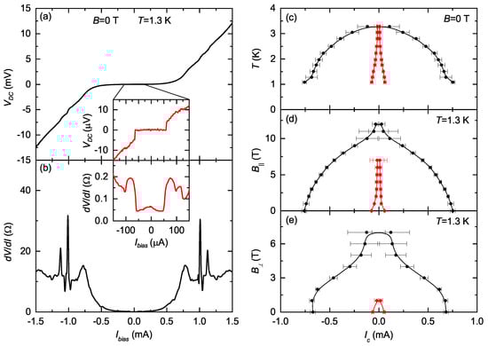
Figure 4.
(a) IV curve of sample 4 measured at T = 1.3 K and B = 0 T. Inset: expanded view on the low-current region where the transition due to the surface can be seen. (b) Differential resistance measured simultaneously with the IV curve. Inset: differential resistance corresponding to the inset of (a). (c–e) Critical currents of the superconducting volume (black) and surface (red) as a function of (c) the temperature, (d) parallel magnetic field and (e) perpendicular magnetic field.
Several clear transitions can be seen in the differential curves shown in Figure 4b. Around 1.0 and 1.1 mA, there are two distinct features that do not lead to a significant change in resistance. We presume that these correspond to parts of the bulk crystal becoming superconducting while others remain resistive and are likely to be a consequence of strong inhomogeneity present in the sample. The transition at 0.7 mA then represents the majority of the bulk crystal becoming normal, leading to a strong increase in the resistivity. The state of zero resistance, however, can only be seen below a much smaller bias current of about 60 A, as seen in the insets of Figure 4a,b. Considering the two-dimensional nature of the superconductivity within the surface layer, this small bias current corresponds to a current density of approximately 8 × A·cm, much larger than that associated with the three-dimensional transition (about 1 × A·cm).
Figure 4c–e shows the transition temperatures and magnetic fields associated with the two- and three-dimensional superconducting phases of the FIB-processed TaP as a function of the critical currents. This is a further confirmation of Figure 3 as the two transitions are suppressed at the same temperature, but at different values of the magnetic field. In perpendicular field, the feature associated with surface superconductivity can be seen up to 1 T, whereas in parallel field it survives up to 7 T. The difference is less apparent for the three-dimensional superconductivity, but also this can be seen to persist to higher fields in the parallel configuration, in agreement with Figure 3b.
3.3. BCS–BEC Crossover Regime
Via Hall effect measurements, the carrier concentration n can be estimated for each of the microstructured samples. As shown in Figure S6a, the Hall resistivity of sample 4 was found to be non-linear, as expected for a semi-metal in which the densities and/or mobilities of the electron- and hole-like carriers are distinct. From the initial slope of , we can nevertheless obtain a maximum value for the density of a single carrier type for each sample. These range from 4.5 × 10 to 3.9 × 10 cm. For a semimetal such as TaP, these are typical values, in agreement with the literature [32,34]. However, for a superconducting material, these are unusually low carrier concentrations. For comparison, we consider SrTiO, for which a carrier concentration of 4.1 × 10 with a of 180 mK has been reported [53]. The of our TaP is at least 10 times higher despite the fact that the carrier densities are comparable. Additionally, the observed characteristic critical fields are relatively high, exceeding the usual Pauli paramagnetic limit. For these reasons, we consider the possibility of a crossover between a Bardeen–Cooper–Schrieffer state and a Bose–Einstein condensate (BCS–BEC) for the observed superconductivity.
Using the value of 7.7 nm for the coherence length obtained from the fitting of Figure 3, we calculate the number of pairs within a coherence volume . In sample 4, this amounts to approximately 25 pairs, suggesting there is limited overlap between the pairs. Typically, a BCS superconductor has many thousands of pairs overlapping within , whereas a BEC superconductor has less than one pair in and there is no interaction between different pairs. With a number of 25 pairs in , sample 4 is similar to FeSe (with 31 pairs [54]), which is considered to reside within the BCS–BEC crossover regime [55,56,57]. These findings therefore suggest that this new breed of semi-metals is a good playground for the observation of possible exotic superconductivity on the BCS–BEC boundary.
4. Conclusions
In conclusion, we have established the existence of three-dimensional, inhomogeneous superconductivity at ambient pressure in a crystal of TaP and confirmed the appearance of FIB-induced two-dimensional surface superconductivity. In other studies, it was found that TaP typically contains a large density of defects and can be off-stoichiometric with an excess of Ta [33,36]. Our EDX data do not exclude off-stoichiometry in our samples, but considering the similarity between the superconducting and non-superconducting samples, any overall off-stoichiometry cannot explain the superconductivity we observe.
It is, however, apparent that our sample is strongly inhomogeneous as we see multiple critical currents associated with partial superconducting transitions, as well as an upturn of the resistance just above the critical field in the parallel field configuration. As such, there may exist domains with a local excess of Ta or defect structures that support superconductivity. Nevertheless, our findings call for a thorough study of the growth of TaP and related compounds in order to establish under what conditions superconductivity can be optimized. Further research is also required to ascertain whether the superconducting volume in TaP retains all the characteristics of a Weyl semimetal. We note here that none of our superconducting crystals exhibited a negative longitudinal magnetoresistance, for example. If it does, however, TaP may provide an ideal platform for the study of Weyl superconductivity.
5. Materials and Methods
5.1. Sample Preparation
The single crystal used in this study was grown by chemical vapor transport using polycrystalline TaP as a source material [37]. Via X-ray crystallography, a facet matching the ab-plane of this crystal was identified and the microsamples were cut from this facet using focused ion beam (FIB) milling. For the rough cutting, an acceleration voltage of 30 kV with a large current of 20 nA was used. Initially, a rectangular piece of the crystal was cut out and remained attached only via a thin bar to the main crystal. A micromanipulator was then brought in contact with the rectangle and fixed onto it via Pt deposition, after which the bar was cut through and the sample was transferred to a silicon oxide substrate with prepatterned gold contact pads. On the substrate, a further shaping of the sample took place at 30 kV and 0.9 nA, followed by a more precise cleaning at 8 kV and 0.2 nA. Contacts were made between the sample and the gold pads via FIB-induced Pt deposition in a standard Hall-bar configuration (see Figure 1b).
5.2. Resistivity Measurements
The resistivity measurements were performed in either a superconducting magnet with a maximum field of 15 T, using a He cryostat, or a resistive magnet of 33 T with a He cryostat with base temperature 1.3 K. We mounted the samples on a rotatable platform in order to vary their angle with the field. Each microsample had six contacts, with the two covering the short ends of the sample being used as current contacts and the other contacts to measure either a longitudinal or a hall voltage. We used an AC current excitation of 10 or 100 A and acquisition took place with standard lock-in techniques. For the measurement of differential resistance, we used a voltage source in series with a 100 k resistor to supply the DC bias current, with the lock-in amplifier similarly supplying a 10 A AC current on top. A multimeter was placed in parallel with the lock-in amplifier to measure the DC signal.
The as-grown sample had an arbitrary shape and so it could not be contacted in any well-defined geometry, making it impossible to determine the absolute resistivity. This sample was measured with four contacts placed along the crystal and a current of 0.5 mA.
5.3. Energy-Dispersive X-ray Analysis (EDX)
In order to determine whether off-stoichiometry might be responsible for the observed superconductivity in our samples, we performed an elemental analysis of the parent crystal together with a non-superconducting crystal of TaP from a different source. The two bulk crystals were measured in the same EDX system during a single run to exclude any difference in signal other than from the material itself. We aligned the crystals by eye to have a flat surface facing the electron beam. To correct for any small discrepancies remaining in the angle between the electron beam and the crystal, both crystals were measured twice with a 180° in-plane rotation in between and the two measurements were averaged. The results before and after the rotation were comparable, suggesting that the orientation and flatness of the surfaces were good.
Despite our best efforts, we could not determine the precise Ta:P ratio with real confidence due to the inherent difficulties associated with quantitative EDX measurements. Such a measurement would require a reference TaP sample that is precisely stoichiometric. While our reference sample is known to be non-superconducting, its stoichiometry is not guaranteed.
5.4. X-ray Diffraction (XRD)
Reflections were measured on a Bruker D8 Quest diffractometer with sealed tube and Triumph monochromator ( = 0.71073 Å). The unit cell was found using the software CELL_ NOW [58]. The XRD pattern is presented in Supplementary Figure S8.
Supplementary Materials
The following are available online at https://www.mdpi.com/2073-4352/10/4/288/s1, Section I: Estimation of uncertainty. Section II: Fitting models. Section III with Table S1: list of sample dimensions. Figure S1: Temperature and field sweeps of all crystals. Figure S2: Illustration of characteristic field identification. Figure S3: Angle dependence of characteristic fields with different fittings. Figure S4: IV curves and of sample 4. Figure S5: IV curves and of sample 4, highlighting the low-current region. Figure S6: Quantum oscillation data of sample 4. Figure S7: Magnetoresistance data of sample 1. Figure S8: Powder XRD spectrum of the parent crystal.
Author Contributions
Conceptualization, M.R.v.D. and S.W.; methodology, M.R.v.D.; validation, M.R.v.D., S.P., N.E.H. and S.W.; formal analysis, M.R.v.D.; investigation, M.R.v.D., S.P., M.K. and P.T.; resources, S.W.; data curation, M.R.v.D.; writing—original draft preparation, M.R.v.D.; writing—review and editing, M.R.v.D., S.P., N.E.H. and S.W.; visualization, M.R.v.D.; supervision, S.W. and N.E.H.; project administration, S.W. and N.E.H.; funding acquisition, S.W. and N.E.H. All authors have read and agreed to the published version of the manuscript.
Funding
This research was supported by the HFML-RU/FOM, member of the European Magnetic Field Laboratory (EMFL).
Acknowledgments
The authors would like to thank Nan Xu for providing the sample used to conduct this study and Andrew Mackenzie for help with the interpretation of the EDX data.
Conflicts of Interest
The authors declare no conflict of interest.
References
- Deng, K.; Wan, G.; Deng, P.; Zhang, K.; Ding, S.; Wang, E.; Yan, M.; Huang, H.; Zhang, H.; Xu, Z.; et al. Experimental observation of topological Fermi arcs in type-II Weyl semimetal MoTe2. Nat. Phys. 2016, 12, 1105–1110. [Google Scholar] [CrossRef]
- Lv, B.Q.; Weng, H.M.; Fu, B.B.; Wang, X.P.; Miao, H.; Ma, J.; Richard, P.; Huang, X.C.; Zhao, L.X.; Chen, G.F.; et al. Discovery of Weyl semimetal TaAs. Phys. Rev. X 2015, 5, 031013. [Google Scholar] [CrossRef]
- Xu, S.Y.; Alidoust, N.; Belopolski, I.; Yuan, Z.; Bian, G.; Chang, T.R.; Zheng, H.; Strocov, V.N.; Sanchez, D.S.; Chang, G.; et al. Discovery of a Weyl fermion state with Fermi arcs in niobium arsenide. Nat. Phys. 2015, 11, 748–754. [Google Scholar] [CrossRef]
- Xu, S.Y.; Belopolski, I.; Alidoust, N.; Neupane, M.; Bian, G.; Zhang, C.; Sankar, R.; Chang, G.; Yuan, Z.; Lee, C.C.; et al. Discovery of a Weyl fermion semimetal and topological Fermi arcs. Science 2015, 349, 613–617. [Google Scholar] [CrossRef]
- Xu, D.F.; Du, Y.P.; Wang, Z.; Li, Y.P.; Niu, X.H.; Yao, Q.; Dudin, P.; Xu, Z.A.; Wan, X.G.; Feng, D.L. Observation of Fermi Arcs in non-Centrosymmetric Weyl Semi-metal Candidate NbP. Chin. Phys. Lett. 2015, 32, 107101. [Google Scholar] [CrossRef]
- Souma, S.; Wang, Z.; Kotaka, H.; Sato, T.; Nakayama, K.; Tanaka, Y.; Kimizuka, H.; Takahashi, T.; Yamauchi, K.; Oguchi, T.; et al. Direct Observation of Nonequivalent Fermi-Arc States of Opposite Surfaces in Noncentrosymmetric Weyl Semimetal NbP. Phys. Rev. B 2016, 93, 161112(R). [Google Scholar] [CrossRef]
- Min, C.H.; Bentmann, H.; Neu, J.N.; Eck, P.; Moser, S.; Figgemeier, T.; Ünzelmann, M.; Kissner, K.; Lutz, P.; Koch, R.J.; et al. Orbital Fingerprint of Topological Fermi Arcs in the Weyl Semimetal TaP. Phys. Rev. Lett. 2019, 122, 116402. [Google Scholar] [CrossRef] [PubMed]
- Niemann, A.C.; Gooth, J.; Wu, S.C.; Bäßler, S.; Sergelius, P.; Hühne, R.; Rellinghaus, B.; Shekhar, C.; Süß, V.; Schmidt, M.; et al. Chiral magnetoresistance in the Weyl semimetal NbP. Sci. Rep. 2017, 7, 43394. [Google Scholar] [CrossRef]
- Huang, X.; Zhao, L.; Long, Y.; Wang, P.; Chen, D.; Yang, Z.; Liang, H.; Xue, M.; Weng, H.; Fang, Z.; et al. Observation of the chiral anomaly induced negative magneto-resistance in 3D Weyl semi-metal TaAs. Phys. Rev. X 2015, 5, 031023. [Google Scholar] [CrossRef]
- Zhang, C.; Xu, S.Y.; Belopolski, I.; Yuan, Z.; Lin, Z.; Tong, B.; Bian, G.; Alidoust, N.; Lee, C.C.; Huang, S.M.; et al. Signatures of the Adler-Bell-Jackiw chiral anomaly in a Weyl Fermion semimetal. Nat. Commun. 2016, 7, 10735. [Google Scholar] [CrossRef]
- Wang, J.; Wang, H.; Li, C.K.; Liu, H.; Yan, J.; Wang, J.; Liu, J.; Lin, Z.; Li, Y.; Wang, Y.; et al. Chiral anomaly and ultrahigh mobility in crystalline HfTe5. Phys. Rev. B 2016, 93, 165127. [Google Scholar] [CrossRef]
- Wang, J.; Li, H.; Chang, C.; He, K.; Lee, J.S.; Lu, H.; Sun, Y.; Ma, X.; Samarth, N.; Shen, S.; et al. Anomalous anisotropic magnetoresistance in topological insulator films. Nano Res. 2012, 5, 739–746. [Google Scholar] [CrossRef]
- Dos Reis, R.D.; Ajeesh, M.O.; Kumar, N.; Arnold, F.; Shekhar, C.; Naumann, M.; Schmidt, M.; Nicklas, M.; Hassinger, E. On the search for the chiral anomaly in Weyl semimetals: The negative longitudinal magnetoresistance. New J. Phys. 2016, 18, 085006. [Google Scholar] [CrossRef]
- Li, Y.; Wang, Z.; Li, P.; Yang, X.; Shen, Z.; Sheng, F.; Li, X.; Lu, Y.; Zheng, Y.; Xu, Z.A. Negative magnetoresistance in Weyl semimetals NbAs and NbP: Intrinsic chiral anomaly and extrinsic effects. Front. Phys. 2017, 12, 127205. [Google Scholar] [CrossRef]
- Naumann, M.; Arnold, F.; Bachmann, M.D.; Modic, K.A.; Moll, P.J.W.; Süß, V.; Schmidt, M.; Hassinger, E. Orbital effect and weak localization physics in the longitudinal magnetoresistance of the Weyl semimetals NbP, NbAs, TaP and TaAs. Phys. Rev. Mater. 2020, 4, 034201. [Google Scholar] [CrossRef]
- Chen, A.; Franz, M. Superconducting proximity effect and Majorana flat bands at the surface of a Weyl semimetal. Phys. Rev. B 2016, 93, 201105. [Google Scholar] [CrossRef]
- Lu, B.; Yada, K.; Sato, M.; Tanaka, Y. Crossed surface flat bands of weyl semimetal superconductors. Phys. Rev. Lett. 2015, 114, 096804. [Google Scholar] [CrossRef]
- Khanna, U.; Kundu, A.; Pradhan, S.; Rao, S. Proximity-induced superconductivity in Weyl semimetals. Phys. Rev. B 2014, 90, 195430. [Google Scholar] [CrossRef]
- Li, Y.; Gu, Q.; Chen, C.; Zhang, J.; Liu, Q.; Hu, X.; Liu, J.; Liu, Y.; Ling, L.; Tian, M.; et al. Nontrivial superconductivity in topological MoTe2−xSx crystals. Proc. Natl. Acad. Sci. USA 2018, 115, 9503–9508. [Google Scholar] [CrossRef]
- Xing, Y.; Shao, Z.; Ge, J.; Wang, J.; Zhu, Z.; Liu, J.; Wang, Y.; Zhao, Z.; Yan, J.; Mandrus, D.; et al. Surface Superconductivity in the type II Weyl Semimetal TaIrTe4. Natl. Sci. Rev. 2019. [Google Scholar] [CrossRef]
- Xu, S.Y.; Belopolski, I.; Sanchez, D.S.; Guo, C.; Chang, G.; Zhang, C.; Bian, G.; Yuan, Z.; Lu, H.; Feng, Y.; et al. Experimental discovery of a topological Weyl semimetal state in TaP. Sci. Adv. 2015, 1, e1501092. [Google Scholar] [CrossRef] [PubMed]
- Huang, S.M.; Xu, S.Y.; Belopolski, I.; Lee, C.C.; Chang, G.; Wang, B.; Alidoust, N.; Bian, G.; Neupane, M.; Zhang, C.; et al. A Weyl Fermion semimetal with surface Fermi arcs in the transition metal monopnictide TaAs class. Nat. Commun. 2015, 6, 7373. [Google Scholar] [CrossRef] [PubMed]
- Shekhar, C.; Nayak, A.K.; Sun, Y.; Schmidt, M.; Nicklas, M.; Leermakers, I.; Zeitler, U.; Skourski, Y.; Wosnitza, J.; Liu, Z.; et al. Extremely large magnetoresistance and ultrahigh mobility in the topological Weyl semimetal candidate NbP. Nat. Phys. 2015, 11, 645–649. [Google Scholar] [CrossRef]
- Aggarwal, L.; Gayen, S.; Das, S.; Kumar, R.; Süß, V.; Shekhar, C.; Felser, C.; Sheet, G. Mesoscopic superconductivity and high spin polarization coexisting at metallic point contacts on the Weyl semimetal TaAs. Nat. Commun. 2017, 8, 13974. [Google Scholar] [CrossRef] [PubMed]
- Wang, H.; Wang, H.; Chen, Y.; Luo, J.; Yuan, Z.; Liu, J.; Wang, Y.; Jia, S.; Liu, X.-J.; Wei, J.; et al. Discovery of tip induced unconventional superconductivity on Weyl semimetal. Sci. Bull. 2017, 62, 425–430. [Google Scholar] [CrossRef]
- Wang, H.; He, Y.; Liu, Y.; Yuan, Z.; Jia, S.; Ma, L.; Liu, X.-J.; Wang, J. Ferromagnetic tip induced unconventional superconductivity in Weyl semimetal. Sci. Bull. 2020, 65, 21–26. [Google Scholar] [CrossRef]
- Luo, J.; Li, Y.; Li, J.; Hashimoto, T.; Kawakami, T.; Lu, H.; Jia, S.; Sato, M.; Wang, J. Surface superconductivity on Weyl semimetal induced by nonmagnetic and ferromagnetic tips. Phys. Rev. Mater. 2019, 3, 124201. [Google Scholar] [CrossRef]
- Li, Y.; Zhou, Y.; Guo, Z.; Chen, X.; Lu, P.; Wang, X.; An, C.; Zhou, Y.; Xing, J.; Du, G.; et al. Concurrence of superconductivity and structure transition in Weyl semimetal TaP under pressure. NPJ Quantum Mater. 2017, 2, 66. [Google Scholar] [CrossRef]
- Kumar, P.; Bhalothia, S.; Patnaik, S. Possible superconductivity in Weyl semimetal NbP. AIP Conf. Proc. 2016, 1731, 140063. [Google Scholar] [CrossRef]
- Baenitz, M.; Schmidt, M.; Suess, V.; Felser, C.; Lüders, K. Superconductivity in Weyl Semimetal NbP: Bulk vs. Surface. J. Phys. Conf. Ser. 2019, 1293, 012002. [Google Scholar] [CrossRef]
- Bachmann, M.D.; Nair, N.; Flicker, F.; Ilan, R.; Meng, T.; Ghimire, N.J.; Bauer, E.D.; Ronning, F.; Analytis, J.G.; Moll, P.J.W. Inducing superconductivity in Weyl semi-metal microstructures by selective ion sputtering. Sci. Adv. 2017, 3, e1602983. [Google Scholar] [CrossRef] [PubMed]
- Arnold, F.; Shekhar, C.; Wu, S.C.; Sun, Y.; dos Reis, R.D.; Kumar, N.; Naumann, M.; Ajeesh, M.O.; Schmidt, M.; Grushin, A.G.; et al. Negative magnetoresistance without well-defined chirality in the Weyl semimetal TaP. Nat. Commun. 2016, 7, 11615. [Google Scholar] [CrossRef] [PubMed]
- Besara, T.; Rhodes, D.A.; Chen, K.W.; Das, S.; Zhang, Q.R.; Sun, J.; Zeng, B.; Xin, Y.; Balicas, L.; Baumbach, R.E.; et al. Coexistence of Weyl Physics and Planar Defects in Semimetals TaP and TaAs. Phys. Rev. B 2016, 93, 245152. [Google Scholar] [CrossRef]
- Du, J.; Wang, H.; Mao, Q.; Khan, R.; Xu, B.; Zhou, Y.; Zhang, Y.; Yang, J.; Chen, B.; Feng, C.; et al. Unsaturated both large positive and negative magnetoresistance in Weyl Semimetal TaP. Sci. China 2016, 59, 657406. [Google Scholar] [CrossRef]
- Hu, J.; Liu, J.Y.; Graf, D.; Radmanesh, S.M.A.; Adams, D.J.; Chuang, A.; Wang, Y.; Chiorescu, I.; Wei, J.; Spinu, L.; et al. π Berry phase and Zeeman splitting of Weyl semimetal TaP. Sci. Rep. 2016, 6, 18674. [Google Scholar] [CrossRef]
- Willerström, J.O. Stacking disorder in NbP, TaP, NbAs and TaAs. J. Less-Common Met. 1984, 99, 273–283. [Google Scholar] [CrossRef]
- Xu, N.; Wang, Z.J.; Weber, A.P.; Magrez, A.; Bugnon, P.; Berger, H.; Matt, C.E.; Ma, J.Z.; Fu, B.B.; Lv, B.Q.; et al. Discovery of Weyl semimetal state violating Lorentz invariance in MoTe2. arXiv 2016, arXiv:1604.02116. [Google Scholar]
- Jaroszynski, J.; Hunte, F.; Balicas, L.; Jo, Y.; Raičević, I.; Gurevich, A.; Larbalestier, D.; Balakirev, F.; Fang, L.; Cheng, P.; et al. Upper critical fields and thermally-activated transport of NdFeAsO0.7F0.3 single crystal. Phys. Rev. B 2008, 78, 174523. [Google Scholar] [CrossRef]
- Santhanam, P.; Chi, C.C.; Wind, S.J.; Brady, M.J.; Bucchignano, J.J. Resistance anomaly near the superconducting transition temperature in short aluminum wires. Phys. Rev. Lett. 1991, 66, 2254. [Google Scholar] [CrossRef]
- Nordström, A.; Rapp, Ö. Resistance-peak anomaly in metallic glasses: Dependence on currents and contact arrangement. Phys. Rev. B 1992, 45, 12577. [Google Scholar] [CrossRef]
- Klimczuk, T.; Plackowski, T.; Sadowski, W.; Plebańczyk, M. A resistivity peak close to Tc in Nd2−xCexCuO4−y single crystals. Phys. C Supercond. 2003, 387, 203–207. [Google Scholar] [CrossRef]
- Wang, J.; Singh, M.; Tian, M.; Kumar, N.; Liu, B.; Shi, C.; Jain, J.K.; Samarth, N.; Mallouk, T.E.; Chan, M.H.W. Interplay between superconductivity and ferromagnetism in crystalline nanowires. Nat. Phys. 2010, 6, 389–394. [Google Scholar] [CrossRef]
- Vaglio, R.; Attanasio, C.; Maritato, L.; Ruosi, A. Explanation of the resistance-peak anomaly in nonhomogeneous superconductors. Phys. Rev. B 1993, 47, 15302. [Google Scholar] [CrossRef] [PubMed]
- Chi, Z.; Chen, X.; An, C.; Yang, L.; Zhao, J.; Feng, Z.; Zhou, Y.; Zhou, Y. Pressure-induced superconductivity in MoP. NPJ Quantum Mater. 2018, 3, 28. [Google Scholar] [CrossRef]
- Tinkham, M. Effect of fluxoid quantization on transition of superconducting films. Phys. Rev. 1963, 129, 2413. [Google Scholar] [CrossRef]
- Tinkham, M. Introduction to Superconductivity, 2nd ed.; McGraw-Hill, Inc.: New York, NY, USA, 1996. [Google Scholar]
- Yamafuji, K.; Kawashima, T.; Irie, F. On the angular dependence of the upper critical field in thin films. Phys. Lett. 1966, 20, 122–123. [Google Scholar] [CrossRef]
- Yamafuji, K.; Kusayanagi, E.; Irie, F. On the angular dependence of the surface superconducting critical field. Phys. Lett. 1966, 21, 11–13. [Google Scholar] [CrossRef]
- Zhang, H.M.; Sun, Y.; Li, W.; Peng, J.P.; Song, C.L.; Xing, Y.; Zhang, Q.; Guan, J.; Li, Z.; Zhao, Y.; et al. Detection of a superconducting phase in a two-atom layer of hexagonal Ga film grown on semiconducting GaN(0001). Phys. Rev. Lett. 2015, 114, 107003. [Google Scholar] [CrossRef]
- Xing, Y.; Zhao, K.; Shan, P.; Zheng, F.; Zhang, Y.; Fu, H.; Liu, Y.; Tian, M.; Xi, C.; Liu, H.; et al. Ising Superconductivity and Quantum Phase Transition in Macro-Size Monolayer NbSe2. Nano Lett. 2017, 17, 6802–6807. [Google Scholar] [CrossRef]
- Lu, J.M.; Zheliuk, O.; Leermakers, I.; Yuan, N.F.Q.; Zeitler, U.; Law, K.T.; Ye, J.T. Evidence for two-dimensional Ising superconductivity in gated MoS2. Science 2015, 350, 1353–1357. [Google Scholar] [CrossRef]
- Ziegler, J.F.; Ziegler, M.D.; Biersack, J.P. SRIM—The stopping and range of ions in matter (2010). Nucl. Instrum. Methods Phys. Res. B 2010, 268, 1818–1823. [Google Scholar] [CrossRef]
- Lin, X.; Zhu, Z.; Fauqué, B.; Behnia, K. Fermi surface of the most dilute superconductor. Phys. Rev. X 2013, 3, 021002. [Google Scholar] [CrossRef]
- Yang, H.; Chen, G.; Zhu, X.; Xing, J.; Wen, H.H. BCS-like critical fluctuations with limited overlap of Cooper pairs in FeSe. Phys. Rev. B 2017, 96, 064501. [Google Scholar] [CrossRef]
- Kasahara, S.; Watashige, T.; Hanaguri, T.; Kohsaka, Y.; Yamashita, T. Field-induced superconducting phase of FeSe in the BCS-BEC cross-over. Proc. Natl. Acad. Sci. USA 2014, 111, 16309–16313. [Google Scholar] [CrossRef] [PubMed]
- Kasahara, S.; Yamashita, T.; Shi, A.; Kobayashi, R.; Shimoyama, Y.; Watashige, T.; Ishida, K.; Terashima, T.; Wolf, T.; Hardy, F.; et al. Giant superconducting fluctuations in the compensated semimetal FeSe at the BCS-BEC crossover. Nat. Commun. 2016, 7, 12843. [Google Scholar] [CrossRef] [PubMed]
- Watashige, T.; Arsenijević, S.; Yamashita, T.; Terazawa, D.; Onishi, T.; Opherden, L.; Kasahara, S.; Tokiwa, Y.; Kasahara, Y.; Shibauchi, T.; et al. Quasiparticle excitations in the superconducting state of FeSe probed by thermal hall conductivity in the vicinity of the BCS-BEC crossover. J. Phys. Soc. Jpn. 2017, 86, 014707. [Google Scholar] [CrossRef]
- Sheldrick, G.M. CELL_NOW; Georg-August-Universität Göttingen: Göttingen, Germany, 2008. [Google Scholar]
© 2020 by the authors. Licensee MDPI, Basel, Switzerland. This article is an open access article distributed under the terms and conditions of the Creative Commons Attribution (CC BY) license (http://creativecommons.org/licenses/by/4.0/).