Recent Advancements in Crystalline Pb-Free Halide Double Perovskites


Abstract
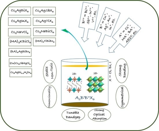
1. Introduction
2. Structural Insight Into Halide Double Perovskites
3. 3D Halide Double Perovskites
3.1. Cs2NaBiCl6
3.2. Cs2AgBiX6 (X = Cl, Br)
3.3. Cs2AgSbX6 (X = Cl, Br)
3.4. Cs2AgInX6 (X = Cl, Br)
3.5. Cs2AgTlX6 (X = Cl, Br)
3.6. Cs2NaVCl6
3.7. Organic–Inorganic Hybrid Halide Double Perovskites
4. 2D Halide Double Perovskites
5. Nanocrystals of Halide Double Perovskites
6. Applications of Halide Double Perovskites
7. Conclusions and Perspectives
Author Contributions
Funding
Conflicts of Interest
References
- Sim, K.; Jun, T.; Bang, J.; Kamioka, H.; Kim, J.; Hiramatsu, H.; Hosono, H. Performance boosting strategy for perovskite light-emitting diodes. Appl. Phys. Rev. 2019, 6, 031402. [Google Scholar] [CrossRef]
- Quan, L.N.; Rand, B.P.; Friend, R.H.; Mhaisalkar, S.G.; Lee, T.-W.; Sargent, E.H. Perovskites for next-generation optical sources. Chem. Rev. 2019, 119, 7444–7477. [Google Scholar] [CrossRef] [PubMed]
- Steele, J.A.; Pan, W.; Martin, C.; Keshavarz, M.; Debroye, E.; Yuan, H.; Banerjee, S.; Fron, E.; Jonckheere, D.; Kim, C.W. Photophysical pathways in highly sensitive Cs2AgBiBr6 double-perovskite single-crystal X-Ray detectors. Adv. Mater. 2018, 30, 1804450. [Google Scholar] [CrossRef] [PubMed]
- Fang, Y.; Dong, Q.; Shao, Y.; Yuan, Y.; Huang, J. Highly narrowband perovskite single-crystal photodetectors enabled by surface-charge recombination. Nat. Photonics 2015, 9, 679. [Google Scholar] [CrossRef]
- Xu, Y.-F.; Yang, M.-Z.; Chen, B.-X.; Wang, X.-D.; Chen, H.-Y.; Kuang, D.-B.; Su, C.-Y. A CsPbBr3 perovskite quantum dot/graphene oxide composite for photocatalytic CO2 reduction. J. Am. Chem. Soc. 2017, 139, 5660–5663. [Google Scholar] [CrossRef] [PubMed]
- Xing, G.; Mathews, N.; Lim, S.S.; Yantara, N.; Liu, X.; Sabba, D.; Grätzel, M.; Mhaisalkar, S.; Sum, T.C. Low-temperature solution-processed wavelength-tunable perovskites for lasing. Nat. Mater. 2014, 13, 476. [Google Scholar] [CrossRef] [PubMed]
- Lian, Z.; Yan, Q.; Gao, T.; Ding, J.; Lv, Q.; Ning, C.; Li, Q.; Sun, J.-L. Perovskite CH3NH3PbI3(Cl) Single crystals: Rapid solution growth, unparalleled crystalline quality, and low trap density toward 108 cm−3. J. Am. Chem. Soc. 2016, 138, 9409–9412. [Google Scholar] [CrossRef]
- Zhang, Z.; Liang, Y.; Huang, H.; Liu, X.; Li, Q.; Chen, L.; Xu, D. Stable and highly efficient photocatalysis with lead-free double-perovskite of Cs2AgBiBr6. Angew. Chem. Int. Ed. 2019, 58, 7263–7267. [Google Scholar] [CrossRef]
- Kojima, A.; Teshima, K.; Shirai, Y.; Miyasaka, T. Organometal halide perovskites as visible-light sensitizers for photovoltaic cells. J. Am. Chem. Soc. 2009, 131, 6050–6051. [Google Scholar] [CrossRef]
- Kim, H.-S.; Lee, C.-R.; Im, J.-H.; Lee, K.-B.; Moehl, T.; Marchioro, A.; Moon, S.-J.; Humphry-Baker, R.; Yum, J.-H.; Moser, J.E. Lead iodide perovskite sensitized all-solid-state submicron thin film mesoscopic solar cell with efficiency exceeding 9%. Sci. Rep. 2012, 2, 591. [Google Scholar] [CrossRef]
- Liu, M.; Johnston, M.B.; Snaith, H.J. Efficient planar heterojunction perovskite solar cells by vapour deposition. Nature 2013, 501, 395. [Google Scholar] [CrossRef] [PubMed]
- Zhou, H.; Chen, Q.; Li, G.; Luo, S.; Song, T.-B.; Duan, H.-S.; Hong, Z.; You, J.; Liu, Y.; Yang, Y. Interface engineering of highly efficient perovskite solar cells. Science 2014, 345, 542–546. [Google Scholar] [CrossRef] [PubMed]
- Jeon, N.J.; Noh, J.H.; Yang, W.S.; Kim, Y.C.; Ryu, S.; Seo, J.; Seok, S.I. Compositional engineering of perovskite materials for high-performance solar cells. Nature 2015, 517, 476–480. [Google Scholar] [CrossRef] [PubMed]
- Saliba, M.; Matsui, T.; Domanski, K.; Seo, J.-Y.; Ummadisingu, A.; Zakeeruddin, S.M.; Correa-Baena, J.-P.; Tress, W.R.; Abate, A.; Hagfeldt, A.; et al. Incorporation of rubidium cations into perovskite solar cells improves photovoltaic performance. Science 2016, 354, 206–209. [Google Scholar] [CrossRef]
- Yang, W.S.; Park, B.-W.; Jung, E.H.; Jeon, N.J.; Kim, Y.C.; Lee, D.U.; Shin, S.S.; Seo, J.; Kim, E.K.; Noh, J.H.; et al. Iodide management in formamidinium-lead-halide–based perovskite layers for efficient solar cells. Science 2017, 356, 1376–1379. [Google Scholar] [CrossRef]
- Jeon, N.J.; Na, H.; Jung, E.H.; Yang, T.-Y.; Lee, Y.G.; Kim, G.; Shin, H.-W.; Il Seok, S.; Lee, J.; Seo, J. A fluorene-terminated hole-transporting material for highly efficient and stable perovskite solar cells. Nat. Energy 2018, 3, 682–689. [Google Scholar] [CrossRef]
- Jung, E.H.; Jeon, N.J.; Park, E.Y.; Moon, C.S.; Shin, T.J.; Yang, T.-Y.; Noh, J.H.; Seo, J. Efficient, stable and scalable perovskite solar cells using poly(3-hexylthiophene). Nature 2019, 567, 511–515. [Google Scholar] [CrossRef]
- National Renewable Energy Laboratory. Best Research Cell Efficiencies. Available online: https://www.nrel.gov/pv/assets/pdfs/best-research-cell-efficiencies.20191106.pdf#opennewwindow (accessed on 22 January 2020).
- Zhao, X.-G.; Yang, J.-H.; Fu, Y.; Yang, D.; Xu, Q.; Yu, L.; Wei, S.-H.; Zhang, L. Design of lead-free inorganic halide perovskites for solar cells via cation-transmutation. J. Am. Chem. Soc. 2017, 139, 2630–2638. [Google Scholar] [CrossRef]
- Filip, M.R.; Hillman, S.; Haghighirad, A.A.; Snaith, H.J.; Giustino, F. Band gaps of the lead-free halide double perovskites Cs2BiAgCl6 and Cs2BiAgBr6 from theory and experiment. J. Phys. Chem. Lett. 2016, 7, 2579–2585. [Google Scholar] [CrossRef]
- McClure, E.T.; Ball, M.R.; Windl, W.; Woodward, P.M. Cs2AgBiX6 (X = Br, Cl): New visible light absorbing, lead-free halide perovskite semiconductors. Chem. Mater. 2016, 28, 1348–1354. [Google Scholar] [CrossRef]
- Noel, N.K.; Stranks, S.D.; Abate, A.; Wehrenfennig, C.; Guarnera, S.; Haghighirad, A.-A.; Sadhanala, A.; Eperon, G.E.; Pathak, S.K.; Johnston, M.B. Lead-free organic-inorganic tin halide perovskites for photovoltaic applications. Energy Environ. Sci. 2014, 7, 3061–3068. [Google Scholar] [CrossRef]
- Roknuzzaman, M.; Ostrikov, K.K.; Wasalathilake, K.C.; Yan, C.; Wang, H.; Tesfamichael, T. Insight into lead-free organic-inorganic hybrid perovskites for photovoltaics and optoelectronics: A first-principles study. J. Org. Electron. 2018, 59, 99–106. [Google Scholar] [CrossRef]
- Filip, M.R.; Giustino, F. Computational screening of homovalent lead substitution in organic-inorganic halide perovskites. J. Phys. Chem. C 2015, 120, 166–173. [Google Scholar] [CrossRef]
- Körbel, S.; Marques, M.A.; Botti, S. Stability and electronic properties of new inorganic perovskites from high-throughput ab initio calculations. J. Mater. Chem. C 2016, 4, 3157–3167. [Google Scholar] [CrossRef]
- Chu, L.; Ahmad, W.; Liu, W.; Yang, J.; Zhang, R.; Sun, Y.; Yang, J.; Li, X.A. Lead-free halide double perovskite materials: A new superstar toward green and stable optoelectronic applications. Nano-Micro Lett. 2019, 11, 16. [Google Scholar] [CrossRef]
- Filip, M.R.; Volonakis, G.; Giustino, F. Hybrid halide perovskites: Fundamental theory and materials design. In Handbook of Materials Modeling: Applications: Current and Emerging Materials; Andreoni, W., Yip, S., Eds.; Springer International Publishing: Cham, Germany, 2018; pp. 1–30. [Google Scholar] [CrossRef]
- Li, T.; Zhao, X.; Yang, D.; Du, M.-H.; Zhang, L. Intrinsic defect properties in halide double perovskites for optoelectronic applications. Phys. Rev. Appl. 2018, 10, 041001. [Google Scholar] [CrossRef]
- Zhao, X.-G.; Yang, D.; Ren, J.-C.; Sun, Y.; Xiao, Z.; Zhang, L. Rational design of halide double perovskites for optoelectronic applications. Joule 2018, 2, 1662–1673. [Google Scholar] [CrossRef]
- Li, Z.; Yin, W. Recent progress in Pb-free stable inorganic double halide perovskites. J. Semicond. 2018, 39, 071003. [Google Scholar] [CrossRef]
- Xiao, Z.; Song, Z.; Yan, Y. From Lead Halide perovskites to lead-free metal halide perovskites and perovskite derivatives. Adv. Mater. 2019, 31, 1803792. [Google Scholar] [CrossRef]
- Zhang, P.; Yang, J.; Wei, S.-H. Manipulation of cation combinations and configurations of halide double perovskites for solar cell absorbers. J. Mater. Chem. A 2018, 6, 1809–1815. [Google Scholar] [CrossRef]
- Goldschmidt, V.M.J.N. Die gesetze der krystallochemie. Naturwissenschaften 1926, 14, 477–485. [Google Scholar] [CrossRef]
- Li, C.; Lu, X.; Ding, W.; Feng, L.; Gao, Y.; Guo, Z. Formability of ABX3 (X = F, Cl, Br, I) halide perovskites. Acta Crystallogr. B 2008, 64, 702–707. [Google Scholar] [CrossRef] [PubMed]
- Ning, W.; Gao, F. Structural and functional diversity in lead-free halide perovskite materials. Adv. Mater. 2019, 31, 1900326. [Google Scholar] [CrossRef] [PubMed]
- Teraoka, Y.; Wei, M.-D.; Kagawa, S. Double perovskites containing hexavalent molybdenum and tungsten: Synthesis, structural investigation and proposal of a fitness factor to discriminate the crystal symmetry. J. Mater. Chem. 1998, 8, 2323–2325. [Google Scholar] [CrossRef]
- Lee, B.; Stoumpos, C.C.; Zhou, N.; Hao, F.; Malliakas, C.; Yeh, C.-Y.; Marks, T.J.; Kanatzidis, M.G.; Chang, R.P. Air-stable molecular semiconducting iodosalts for solar cell applications: Cs2SnI6 as a hole conductor. J. Am. Chem. Soc. 2014, 136, 15379–15385. [Google Scholar] [CrossRef]
- Luo, J.; Wang, X.; Li, S.; Liu, J.; Guo, Y.; Niu, G.; Yao, L.; Fu, Y.; Gao, L.; Dong, Q.; et al. Efficient and stable emission of warm-white light from lead-free halide double perovskites. Nature 2018, 563, 541–545. [Google Scholar] [CrossRef]
- Du, K.-Z.; Wang, X.; Han, Q.; Yan, Y.; Mitzi, D.B. Heterovalent B-site co-alloying approach for halide perovskite bandgap engineering. ACS Energy Lett. 2017, 2, 2486–2490. [Google Scholar] [CrossRef]
- Karmakar, A.; Dodd, M.S.; Agnihotri, S.; Ravera, E.; Michaelis, V.K. Cu(II)-doped Cs2SbAgCl6 double perovskite: A lead-free, low-bandgap material. Chem. Mater. 2018, 30, 8280–8290. [Google Scholar] [CrossRef]
- Liu, W.; Lin, Q.; Li, H.; Wu, K.; Robel, I.; Pietryga, J.M.; Klimov, V.I. Mn2+-doped lead halide perovskite nanocrystals with dual-color emission controlled by halide content. J. Am. Chem. Soc. 2016, 138, 14954–14961. [Google Scholar] [CrossRef]
- Tan, Z.; Li, J.; Zhang, C.; Li, Z.; Hu, Q.; Xiao, Z.; Kamiya, T.; Hosono, H.; Niu, G.; Lifshitz, E. Highly efficient blue-emitting Bi-doped Cs2SnCl6 perovskite variant: Photoluminescence induced by impurity doping. Adv. Funct. Mater. 2018, 28, 1801131. [Google Scholar] [CrossRef]
- Bagnall, K.; Laidler, J.; Stewart, M. Americium chloro-complexes. J. Chem. Soc. 1968, 133–136. [Google Scholar] [CrossRef]
- Morss, L.R.; Siegal, M.; Stenger, L.; Edelstein, N. Preparation of cubic chloro complex compounds of trivalent metals: Cs2NaMCl6. Inorg. Chem. 1970, 9, 1771–1775. [Google Scholar] [CrossRef]
- Morrs, L.; Robinson, W. Crystal structure of Cs2NaBiCl6. Acta Crystallogr. B 1972, 28, 653–654. [Google Scholar] [CrossRef]
- Pelle, F.; Jacquier, B.; Denis, J.; Blanzat, B. Optical properties of Cs2NaBiCl6. J. Lumin. 1978, 17, 61–72. [Google Scholar] [CrossRef]
- Pelle, F.; Blanzat, B.; Chevalier, B. Low temperature phase transition in cubic elpasolithe crystal Cs2NaBiCl6. Solid State Commun. 1984, 49, 1089–1093. [Google Scholar] [CrossRef]
- Majher, J.D.; Gray, M.B.; Strom, T.A.; Woodward, P.M. Cs2NaBiCl6:Mn2+—A new orange-red halide double perovskite phosphor. Chem. Mater. 2019, 31, 1738–1744. [Google Scholar] [CrossRef]
- Slavney, A.H.; Hu, T.; Lindenberg, A.M.; Karunadasa, H.I. A bismuth-halide double perovskite with long carrier recombination lifetime for photovoltaic applications. J. Am. Chem. Soc. 2016, 138, 2138–2141. [Google Scholar] [CrossRef]
- Pan, W.; Wu, H.; Luo, J.; Deng, Z.; Ge, C.; Chen, C.; Jiang, X.; Yin, W.-J.; Niu, G.; Zhu, L. Cs2AgBiBr6 single-crystal X-ray detectors with a low detection limit. Nat. Photonics 2017, 11, 726. [Google Scholar] [CrossRef]
- Savory, C.N.; Walsh, A.; Scanlon, D.O. Can Pb-free halide double perovskites support high-efficiency solar cells? ACS Energy Lett. 2016, 1, 949–955. [Google Scholar] [CrossRef]
- Saparov, B.; Sun, J.-P.; Meng, W.; Xiao, Z.; Duan, H.-S.; Gunawan, O.; Shin, D.; Hill, I.G.; Yan, Y.; Mitzi, D.B. Thin-film deposition and characterization of a Sn-deficient perovskite derivative Cs2SnI6. Chem. Mater. 2016, 28, 2315–2322. [Google Scholar] [CrossRef]
- Schade, L.; Wright, A.D.; Johnson, R.D.; Dollmann, M.; Wenger, B.; Nayak, P.K.; Prabhakaran, D.; Herz, L.M.; Nicholas, R.; Snaith, H.J.; et al. Structural and optical properties of Cs2AgBiBr6 double perovskite. ACS Energy Lett. 2019, 4, 299–305. [Google Scholar] [CrossRef]
- Lan, C.; Zhao, S.; Luo, J.; Fan, P. First-principles study of anion diffusion in lead-free halide double perovskites. Phys. Chem. Chem. Phys. 2018, 20, 24339–24344. [Google Scholar] [CrossRef] [PubMed]
- Steele, J.A.; Puech, P.; Keshavarz, M.; Yang, R.; Banerjee, S.; Debroye, E.; Kim, C.W.; Yuan, H.; Heo, N.H.; Vanacken, J. Giant electron–phonon coupling and deep conduction band resonance in metal halide double perovskite. ACS Nano 2018, 12, 8081–8090. [Google Scholar] [CrossRef] [PubMed]
- Kung, P.-K.; Li, M.-H.; Lin, P.-Y.; Jhang, J.-Y.; Pantaler, M.; Lupascu, D.C.; Grancini, G.; Chen, P. Lead-free double perovskites for perovskite solar cells. Solar RRL 2020. [Google Scholar] [CrossRef]
- Hutter, E.M.; Gélvez-Rueda, M.C.; Bartesaghi, D.; Grozema, F.C.; Savenije, T.J. Band-like charge transport in Cs2AgBiBr6 and mixed antimony-bismuth Cs2AgBi1−xSbxBr6 halide double perovskites. ACS Omega 2018, 3, 11655–11662. [Google Scholar] [CrossRef]
- Du, K.-Z.; Meng, W.; Wang, X.; Yan, Y.; Mitzi, D.B. Bandgap engineering of lead-free double perovskite Cs2AgBiBr6 through trivalent metal alloying. Angew. Chem. Int. Ed. 2017, 56, 8158–8162. [Google Scholar] [CrossRef]
- Vegard, L.J.Z.F.P. Die Konstitution der Mischkristalle und die Raumfüllung der Atome. Zeitschrift Für Physik 1921, 5, 17–26. [Google Scholar] [CrossRef]
- Slavney, A.H.; Leppert, L.; Bartesaghi, D.; Gold-Parker, A.; Toney, M.F.; Savenije, T.J.; Neaton, J.B.; Karunadasa, H.I. Defect-induced band-edge reconstruction of a bismuth-halide double perovskite for visible-light absorption. J. Am. Chem. Soc. 2017, 139, 5015–5018. [Google Scholar] [CrossRef]
- Volonakis, G.; Filip, M.R.; Haghighirad, A.A.; Sakai, N.; Wenger, B.; Snaith, H.J.; Giustino, F. Lead-free halide double perovskites via heterovalent substitution of noble metals. J. Phys. Chem. Lett. 2016, 7, 1254–1259. [Google Scholar] [CrossRef]
- Wei, F.; Deng, Z.; Sun, S.; Hartono, N.T.P.; Seng, H.L.; Buonassisi, T.; Bristowe, P.D.; Cheetham, A.K. Enhanced visible light absorption for lead-free double perovskite Cs2AgSbBr6. Chem. Commun. 2019, 55, 3721–3724. [Google Scholar] [CrossRef]
- Deng, W.; Deng, Z.-Y.; He, J.; Wang, M.; Chen, Z.-X.; Wei, S.-H.; Feng, H.-J. Synthesis of Cs2AgSbCl6 and improved optoelectronic properties of Cs2AgSbCl6/TiO2 heterostructure driven by the interface effect for lead-free double perovskites solar cells. Appl. Phys. Lett. 2017, 111, 151602. [Google Scholar] [CrossRef]
- Volonakis, G.; Haghighirad, A.A.; Milot, R.L.; Sio, W.H.; Filip, M.R.; Wenger, B.; Johnston, M.B.; Herz, L.M.; Snaith, H.J.; Giustino, F. Cs2InAgCl6: A new lead-free halide double perovskite with direct band gap. J. Phys. Chem. Lett. 2017, 8, 772–778. [Google Scholar] [CrossRef] [PubMed]
- Tran, T.T.; Panella, J.R.; Chamorro, J.R.; Morey, J.R.; McQueen, T.M. Designing indirect-direct bandgap transitions in double perovskites. Mater. Horiz. 2017, 4, 688–693. [Google Scholar] [CrossRef]
- Hutter, E.M.; Gélvez-Rueda, M.C.; Osherov, A.; Bulović, V.; Grozema, F.C.; Stranks, S.D.; Savenije, T.J. Direct-indirect character of the bandgap in methylammonium lead iodide perovskite. Nat. Mater. 2017, 16, 115. [Google Scholar] [CrossRef] [PubMed]
- Zhou, J.; Xia, Z.; Molokeev, M.S.; Zhang, X.; Peng, D.; Liu, Q. Composition design, optical gap and stability investigations of lead-free halide double perovskite Cs2AgInCl6. J. Mater. Chem. A 2017, 5, 15031–15037. [Google Scholar] [CrossRef]
- Luo, J.; Li, S.; Wu, H.; Zhou, Y.; Li, Y.; Liu, J.; Li, J.; Li, K.; Yi, F.; Niu, G.; et al. Cs2AgInCl6 double perovskite single crystals: Parity forbidden transitions and their application for sensitive and fast UV photodetectors. ACS Photonics 2018, 5, 398–405. [Google Scholar] [CrossRef]
- Weng, W.Y.; Chang, S.J.; Hsu, C.L.; Hsueh, T.J. A ZnO-nanowire phototransistor prepared on glass substrates. ACS Appl. Mater. Interfaces 2011, 3, 162–166. [Google Scholar] [CrossRef]
- Nag, A. Synthesis and luminescence of Mn-doped Cs2AgInCl6 double perovskites. Chem. Commun. 2018, 54, 5205–5208. [Google Scholar]
- Nie, X.; Wei, S.-H.; Zhang, S. Bipolar doping and band-gap anomalies in delafossite transparent conductive oxides. Phys. Rev. Lett. 2002, 88, 066405. [Google Scholar] [CrossRef]
- Walsh, A.; Da Silva, J.L.; Wei, S.-H.; Körber, C.; Klein, A.; Piper, L.; DeMasi, A.; Smith, K.E.; Panaccione, G.; Torelli, P. Nature of the band gap of In2O3 revealed by first-principles calculations and x-ray spectroscopy. Phys. Rev. Lett. 2008, 100, 167402. [Google Scholar] [CrossRef]
- Kehoe, A.B.; Scanlon, D.O.; Watson, G.W. Nature of the band gap of Tl2O3. Phys. Rev. B 2011, 83, 233202. [Google Scholar] [CrossRef]
- Summitt, R.; Marley, J.A.; Borrelli, N.F. The ultraviolet absorption edge of stannic oxide (SnO2). J. Phys. Chem. Solids 1964, 25, 1465–1469. [Google Scholar] [CrossRef]
- Meng, W.; Wang, X.; Xiao, Z.; Wang, J.; Mitzi, D.B.; Yan, Y. Parity-forbidden transitions and their impact on the optical absorption properties of lead-free metal halide perovskites and double perovskites. J. Phys. Chem. Lett. 2017, 8, 2999–3007. [Google Scholar] [CrossRef] [PubMed]
- Slavney, A.H.; Leppert, L.; Saldivar Valdes, A.; Bartesaghi, D.; Savenije, T.J.; Neaton, J.B.; Karunadasa, H.I. Small-band-gap halide double perovskites. Angew. Chem. Int. Ed. 2018, 57, 12765–12770. [Google Scholar] [CrossRef] [PubMed]
- Cao, X.; Kang, L.; Guo, S.; Zhang, M.; Lin, Z.; Gao, J. Cs2NaVCl6: A Pb-free halide double perovskite with strong visible and near-infrared light absorption. ACS Appl. Mater. Interfaces 2019, 11, 38648–38653. [Google Scholar] [CrossRef]
- Deng, Z.; Wei, F.; Sun, S.; Kieslich, G.; Cheetham, A.K.; Bristowe, P.D. Exploring the properties of lead-free hybrid double perovskites using a combined computational-experimental approach. J. Mater. Chem. A 2016, 4, 12025–12029. [Google Scholar] [CrossRef]
- Slavney, A.H.; Connor, B.A.; Leppert, L.; Karunadasa, H.I. A pencil-and-paper method for elucidating halide double perovskite band structures. Chem. Sci. 2019, 10, 11041–11053. [Google Scholar] [CrossRef]
- Wei, F.; Deng, Z.; Sun, S.; Xie, F.; Kieslich, G.; Evans, D.M.; Carpenter, M.A.; Bristowe, P.D.; Cheetham, A.K. The synthesis, structure and electronic properties of a lead-free hybrid inorganic–organic double perovskite (MA)2KBiCl6 (MA = methylammonium). Mater. Horiz. 2016, 3, 328–332. [Google Scholar] [CrossRef]
- Li, Y.-J.; Wu, T.; Sun, L.; Yang, R.-X.; Jiang, L.; Cheng, P.-F.; Hao, Q.-Q.; Wang, T.-J.; Lu, R.-F.; Deng, W.-Q. Lead-free and stable antimony–silver-halide double perovskite (CH3NH3)2AgSbI6. RSC Adv. 2017, 7, 35175–35180. [Google Scholar] [CrossRef]
- Volonakis, G.; Haghighirad, A.A.; Snaith, H.J.; Giustino, F. Route to stable lead-free double perovskites with the electronic structure of CH3NH3PbI3: A case for mixed-cation [Cs/CH3NH3/CH(NH2)2]2InBiBr6. J. Phys. Chem. Lett. 2017, 8, 3917–3924. [Google Scholar] [CrossRef]
- Mao, L.; Teicher, S.M.L.; Stoumpos, C.C.; Kennard, R.M.; DeCrescent, R.A.; Wu, G.; Schuller, J.A.; Chabinyc, M.L.; Cheetham, A.K.; Seshadri, R. Chemical and structural diversity of hybrid layered double perovskite halides. J. Am. Chem. Soc. 2019, 141, 19099–19109. [Google Scholar] [CrossRef] [PubMed]
- Tang, G.; Xiao, Z.; Hong, J. Designing two-dimensional properties in three-dimensional halide perovskites via orbital engineering. J. Phys. Chem. Lett. 2019, 10, 6688–6694. [Google Scholar] [CrossRef] [PubMed]
- Connor, B.A.; Leppert, L.; Smith, M.D.; Neaton, J.B.; Karunadasa, H.I. Layered halide double perovskites: Dimensional reduction of Cs2AgBiBr6. J. Am. Chem. Soc. 2018, 140, 5235–5240. [Google Scholar] [CrossRef] [PubMed]
- Xu, Z.; Liu, X.; Li, Y.; Liu, X.; Yang, T.; Ji, C.; Han, S.; Xu, Y.; Luo, J.; Sun, Z. Exploring lead-free hybrid double perovskite crystals of (BA)2CsAgBiBr7 with large mobility-lifetime product toward X-Ray detection. Angew. Chem. Int. Ed. 2019, 58, 15757–15761. [Google Scholar] [CrossRef]
- Fang, Y.; Zhang, L.; Wu, L.; Yan, J.; Lin, Y.; Wang, K.; Mao, W.L.; Zou, B. Pressure-induced emission (PIE) and phase transition of a two-dimensional halide double perovskite (BA)4AgBiBr8 (BA = CH3(CH2)3NH3+). Angew. Chem. Int. Ed. 2019, 58, 15249–15253. [Google Scholar] [CrossRef]
- Bi, L.-Y.; Hu, Y.-Q.; Li, M.-Q.; Hu, T.-L.; Zhang, H.-L.; Yin, X.-T.; Que, W.-X.; Lassoued, M.S.; Zheng, Y.-Z. Two-dimensional lead-free iodide-based hybrid double perovskites: Crystal growth, thin-film preparation and photocurrent responses. J. Mater. Chem. A 2019, 7, 19662–19667. [Google Scholar] [CrossRef]
- Swarnkar, A.; Ravi, V.K.; Nag, A. Beyond colloidal cesium lead halide perovskite nanocrystals: Analogous metal halides and doping. ACS Energy Lett. 2017, 2, 1089–1098. [Google Scholar] [CrossRef]
- Zhou, L.; Xu, Y.F.; Chen, B.X.; Kuang, D.B.; Su, C.Y. Synthesis and photocatalytic application of stable lead-free Cs2AgBiBr6 perovskite nanocrystals. Small 2018, 14, 1703762. [Google Scholar] [CrossRef]
- Creutz, S.E.; Crites, E.N.; De Siena, M.C.; Gamelin, D.R. Colloidal nanocrystals of lead-free double-perovskite (elpasolite) semiconductors: Synthesis and anion exchange to access new materials. Nano Lett. 2018, 18, 1118–1123. [Google Scholar] [CrossRef]
- Bekenstein, Y.; Dahl, J.C.; Huang, J.; Osowiecki, W.T.; Swabeck, J.K.; Chan, E.M.; Yang, P.; Alivisatos, A.P. The making and breaking of lead-free double perovskite nanocrystals of cesium silver–bismuth halide compositions. Nano Lett. 2018, 18, 3502–3508. [Google Scholar] [CrossRef]
- Lignos, I.; Stavrakis, S.; Nedelcu, G.; Protesescu, L.; deMello, A.J.; Kovalenko, M.V. Synthesis of cesium lead halide perovskite nanocrystals in a droplet-based microfluidic platform: Fast parametric space mapping. Nano Lett. 2016, 16, 1869–1877. [Google Scholar] [CrossRef] [PubMed]
- Brittman, S.; Luo, J. A promising beginning for perovskite nanocrystals: A Nano Letters virtual issue. Nano Lett. 2018, 18, 2747–2750. [Google Scholar] [CrossRef] [PubMed]
- Mir, W.J.; Jagadeeswararao, M.; Das, S.; Nag, A. Colloidal Mn-doped cesium lead halide perovskite nanoplatelets. ACS Energy Lett. 2017, 2, 537–543. [Google Scholar] [CrossRef]
- Shamsi, J.; Urban, A.S.; Imran, M.; De Trizio, L.; Manna, L. Metal halide perovskite nanocrystals: Synthesis, post-synthesis modifications, and their optical properties. Chem. Rev. 2019, 119, 3296–3348. [Google Scholar] [CrossRef]
- Yang, B.; Mao, X.; Hong, F.; Meng, W.; Tang, Y.; Xia, X.; Yang, S.; Deng, W.; Han, K. Lead-free direct band gap double-perovskite nanocrystals with bright-color emission. J. Am. Chem. Soc. 2018, 140, 17001–17006. [Google Scholar] [CrossRef]
- Yang, B.; Chen, J.; Yang, S.; Hong, F.; Sun, L.; Han, P.; Pullerits, T.; Deng, W.; Han, K. Lead-free silver-bismuth halide double perovskite nanocrystals. Angew. Chem. Int. Ed. 2018, 57, 5359–5363. [Google Scholar] [CrossRef]
- Hao, F.; Stoumpos, C.C.; Cao, D.H.; Chang, R.P.; Kanatzidis, M.G. Lead-free solid-state organic-inorganic halide perovskite solar cells. Nat. Photonics 2014, 8, 489. [Google Scholar] [CrossRef]
- Pantaler, M.; Cho, K.T.; Queloz, V.I.E.; García Benito, I.; Fettkenhauer, C.; Anusca, I.; Nazeeruddin, M.K.; Lupascu, D.C.; Grancini, G. Hysteresis-free lead-free double-perovskite solar cells by interface engineering. ACS Energy Lett. 2018, 3, 1781–1786. [Google Scholar] [CrossRef]
- Zhang, J.; Bai, D.; Jin, Z.; Bian, H.; Wang, K.; Sun, J.; Wang, Q.; Liu, S. 3D–2D–0D interface profiling for record efficiency all-inorganic CsPbBrI2 perovskite solar cells with superior stability. Adv. Energy Mater. 2018, 8, 1703246. [Google Scholar] [CrossRef]
- Greul, E.; Petrus Michiel, L.; Binek, A.; Docampo, P.; Bein, T. Highly stable, phase pure Cs2AgBiBr6 double perovskite thin films for optoelectronic applications. J. Mater. Chem. A 2017, 5, 19972–19981. [Google Scholar] [CrossRef]
- Volonakis, G.; Giustino, F. Surface properties of lead-free halide double perovskites: Possible visible-light photo-catalysts for water splitting. Appl. Phys. Lett. 2018, 112, 243901. [Google Scholar] [CrossRef]
- Zhao, L.; Kerner, R.A.; Xiao, Z.; Lin, Y.L.; Lee, K.M.; Schwartz, J.; Rand, B.P. Redox chemistry dominates the degradation and decomposition of metal halide perovskite optoelectronic devices. ACS Energy Lett. 2016, 1, 595–602. [Google Scholar] [CrossRef]
- Tiong, V.T.; Pham, N.D.; Wang, T.; Zhu, T.; Zhao, X.; Zhang, Y.; Shen, Q.; Bell, J.; Hu, L.; Dai, S. Octadecylamine-functionalized single-walled carbon nanotubes for facilitating the formation of a monolithic perovskite layer and stable solar cells. Adv. Funct. Mater. 2018, 28, 1705545. [Google Scholar] [CrossRef]


| Double Perovskite | Crystal System | Space Group | Bandgap (eV) | PL (eV) | Synthetic Method | Reference |
|---|---|---|---|---|---|---|
| Cs2AgBiBr6 | Cubic | Fmm | 2.19 indirect | 1.87 | Hydrothermal | [21,49] |
| Cs2AgBiCl6 | Cubic | Fmm | 2.77 indirect | 3.14 | Solid-state and hydrothermal | [21,61,98] |
| (MA)2KBiCl6 | Rhombohedral | Rm | 3.04 indirect | Hydrothermal | [80] | |
| (MA)2TlBiBr6 | Cubic | Fmm | ~2.0 direct | Hydrothermal | [78] | |
| Cs2AgInCl6 | Cubic | Fmm | 3.23 direct | 1.95 | Solid-state and hydrothermal | [65,67,75] |
| Cs2AgSbCl6 | Cubic | Fmm | 2.54–2.60 indirect | Hydrothermal | [63,65] | |
| Cs2AgIn0.5Sb0.5Cl6 | 2.81 indirect | Hydrothermal | [65] | |||
| Cs2AgSb0.4In0.6Cl6 | 2.92 direct | Hydrothermal | [65] | |||
| Cs2AgSb0.2In0.8Cl6 | 3.06 direct | Hydrothermal | [65] | |||
| Cs2NaVCl6 | Cubic | Fmm | ~2.64 direct | Solid-state | [77] | |
| Cs2AgBi1–xSbxBr6 | Cubic | Fmm | 2–1.6 | Solid-state | [57] | |
| (MA)2AgSbI6 | Cubic | Fmm | 1.93 | Solid-state | [81] | |
| Cs2AgSbBr6 | Cubic | Fmm | 1.64 indirect | Hydrothermal | [62] | |
| Cs2NaBiCl6 | Cubic | Fmm | Solvent evaporation | [44,45] | ||
| PA4AgInCl8 | Triclinic | P | 3.96 | Hydrothermal | [83] | |
| PA4AgBiBr8 | Monoclinic | C2/m | 2.41 | Hydrothermal | [83] | |
| PA4AgInBr8 | Monoclinic | C2/m | 3.15 | 2.76 | Hydrothermal | [83] |
| OCA4AgBiBr8 | Monoclinic | C2/m | Hydrothermal | [83] | ||
| BDA2AgBiBr8 | Triclinic | P | Hydrothermal | [83] | ||
| PA2CsAgBiBr7 | Monoclinic | C2/m | Hydrothermal | [83] | ||
| PA2CsAgIn0.5Bi0.5Br7 | Monoclinic | C2/m | Hydrothermal | [83] | ||
| PA4AgSb0.5Bi0.5Br8 | 2.51 | 1.93 | Hydrothermal | [83] | ||
| PA4AgIn0.5Bi0.5Br8 | 2.56 | 1.76 | Hydrothermal | [83] |
© 2020 by the authors. Licensee MDPI, Basel, Switzerland. This article is an open access article distributed under the terms and conditions of the Creative Commons Attribution (CC BY) license (http://creativecommons.org/licenses/by/4.0/).
Share and Cite
Usman, M.; Yan, Q. Recent Advancements in Crystalline Pb-Free Halide Double Perovskites. Crystals 2020, 10, 62. https://doi.org/10.3390/cryst10020062
Usman M, Yan Q. Recent Advancements in Crystalline Pb-Free Halide Double Perovskites. Crystals. 2020; 10(2):62. https://doi.org/10.3390/cryst10020062
Chicago/Turabian StyleUsman, Muhammad, and Qingfeng Yan. 2020. "Recent Advancements in Crystalline Pb-Free Halide Double Perovskites" Crystals 10, no. 2: 62. https://doi.org/10.3390/cryst10020062
APA StyleUsman, M., & Yan, Q. (2020). Recent Advancements in Crystalline Pb-Free Halide Double Perovskites. Crystals, 10(2), 62. https://doi.org/10.3390/cryst10020062