Article

Comparison of Hafnium Dioxide and Zirconium Dioxide Grown by Plasma-Enhanced Atomic Layer Deposition for the Application of Electronic Materials

1
Department of Electrical Engineering, Alabama A&M University, Normal, AL 35762, USA
2
Center for Functional Nanomaterials, Brookhaven National Laboratory, Upton, NY 11973, USA
*
Author to whom correspondence should be addressed.
Crystals 2020, 10(2), 136; https://doi.org/10.3390/cryst10020136
Submission received: 27 January 2020 / Revised: 19 February 2020 / Accepted: 20 February 2020 / Published: 23 February 2020
(This article belongs to the Section Crystalline Materials)

Abstract

:
We report the growth of nanoscale hafnium dioxide (HfO2) and zirconium dioxide (ZrO2) thin films using remote plasma-enhanced atomic layer deposition (PE-ALD), and the fabrication of complementary metal-oxide semiconductor (CMOS) integrated circuits using the HfO2 and ZrO2 thin films as the gate oxide. Tetrakis (dimethylamino) hafnium (Hf[N(CH3)2]4) and tetrakis (dimethylamino) zirconium (IV) (Zr[N(CH3)2]4) were used as the precursors, while O2 gas was used as the reactive gas. The PE-ALD-grown HfO2 and ZrO2 thin films were analyzed using X-ray photoelectron spectroscopy (XPS), X-ray diffraction (XRD), and high-resolution transmission electron microscopy (HRTEM). The XPS measurements show that the ZrO2 film has the atomic concentrations of 34% Zr, 2% C, and 64% O while the HfO2 film has the atomic concentrations of 29% Hf, 11% C, and 60% O. The HRTEM and XRD measurements show both HfO2 and ZrO2 films have polycrystalline structures. n-channel and p-channel metal-oxide semiconductor field-effect transistors (nFETs and pFETs), CMOS inverters, and CMOS ring oscillators were fabricated to test the quality of the HfO2 and ZrO2 thin films as the gate oxide. Current-voltage (IV) curves, transfer characteristics, and oscillation waveforms were measured from the fabricated transistors, inverters, and oscillators, respectively. The experimental results measured from the HfO2 and ZrO2 thin films were compared.

1. Introduction

This paper reports the results of remote plasma-enhanced atomic layer deposition (PE-ALD) of nanoscale hafnium dioxide (HfO2) and zirconium dioxide (ZrO2) thin films using tetrakis (dimethylamino) hafnium (Hf[N(CH3)2]4) and tetrakis (dimethylamino) zirconium (IV) (Zr[N(CH3)2]4) as the deposition precursors and oxygen as the reactive gas, and the fabrication of complementary metal-oxide semiconductor (CMOS) integrated circuits using the PE-ALD-grown HfO2 and ZrO2 as the gate oxide. The objectives were to grow hafnium dioxide (HfO2) and zirconium dioxide (ZrO2) thin films at moderate substrate temperatures (200–400 °C) for the application of high dielectric constant (κ) oxide, to compare the two PE-ALD-grown metal oxides, and to test their functionality and performance as the gate oxide in the fabrication of CMOS integrated circuits.
High-κ metal oxides such as hafnium dioxide (HfO2) and zirconium dioxide (ZrO2) thin films have been used as the gate oxide in the fabrication of metal-oxide-semiconductor field-effect transistors (MOSFETs) due to their high dielectric constant (κ) [1,2,3,4,5]. As MOSFETs are scaled down to nanometer sizes, the tunneling currents through the gate dielectrics (the gate leakage current) have become a major concern in today’s fabrication of integrated circuits (ICs). High-κ dielectric metal oxide could be a solution to the problem of the gate leakage current. The equivalent oxide thickness (EOT) of the gate dielectric in MOSFETs is: EOT = (κSiO2/κ)Tphys, where κSiO2 = 3.9. An oxide with a higher dielectric constant (κ) has a relatively larger physical thickness (Tphys) for an equivalent oxide thickness, thereby lowering the gate leakage current. Hafnium dioxide (HfO2) and zirconium dioxide (ZrO2) thin films can be grown using various techniques, such as physical vapor deposition (PVD) [6,7], chemical vapor deposition (CVD) [8,9], plasma-enhanced chemical vapor deposition (PE-CVD) [10,11], and, more recently, atomic layer deposition (ALD) [12,13,14,15,16,17,18] and plasma-enhanced atomic layer deposition (PE-ALD) [19,20]. PVD, such as sputtering, is a clean process without applying chemicals in the process chamber; however, the thin films deposited may have poor conformity. Thermal CVD relies on thermal energy to activate gas-phase and surface reactions. High temperatures between 600 and 1000 °C are usually required for CVD. Plasma-enhanced chemical vapor deposition (PE-CVD) is an extension of thermal CVD in which gas-phase plasma electron impact is substituted for thermal agitation, thereby achieving much lower substrate temperatures [21,22,23]. The ALD process is similar to the CVD process and uses chemical precursors for the deposition of materials. ALD can produce conformal and ultra-thin films with precise thickness control at the atomic layer level [24,25,26,27]. The PE-ALD process is similar to the PE-CVD process, and has the advantage of the gas-phase plasma electron impact on the deposition to assist the dissociation of chemicals for active species; therefore, plasma-enhanced ALD can deposit films at much lower temperatures than thermal ALD [28,29].
There has been extensive research on the growth of metal oxides and their application in the fabrication of electronic devices [30,31,32]. Miniaturization in the modern semiconductor industry requires thin film deposition to have atomic level control and the deposited film to be conformal and pinhole-free. The plasma-enhanced atomic layer deposition of HfO2 and ZrO2 thin films meets these requirements and could be used for the growth of a high dielectric constant (κ) gate oxide in the fabrication of integrated circuits (ICs).

2. Experimental Details

Tetrakis (dimethylamino) hafnium (Hf[N(CH3)2]4) (TDMAH, 99% purity) and tetrakis (dimethylamino) zirconium (IV) (Zr[N(CH3)2]4) (TDMAZ, 99% purity) from Stream Chemicals (Newburyport, MA, USA), Inc. were used as the precursors, and oxygen was used as reactive gas for the synthesis of the hafnium dioxide (HfO2) and zirconium dioxide (ZrO2) thin films. An ALD-150LX system, which was manufactured by the Kurt J. Lesker Company (Jefferson Hills, PA, USA), was used to grow the films. The ALD system comprises a main process chamber, a vacuum load-lock for sample introduction, a remote plasma source, and a pumping system. Substrates were loaded into the load lock and transferred to the ALD chamber. The load lock was pumped by a 210 L/s turbo pump backed by a mechanical pump and had a base pressure of 5 × 10⁻⁷ Torr. The process chamber was evacuated by a 70 cfm chemical series water-cooled rotary screw dry pump. An inductively coupled remote plasma source (13.56 MHz, 0–1000 W) was used to generate high-density plasma for the synthesis of materials in the system. The substrate holder stage was heated at 270 °C for the deposition of HfO2 and ZrO2 films. The precursor bottle for TDMAH was heated at 85 °C, while the precursor bottle for TDMAZ was heated at 75 °C. Reactant delivery lines for the delivery of precursors was heated at 100 °C. Carrier gas mass flow controllers (MFC), high-speed ALD valves, and shut off valves were used to control the flow of carrier gas, precursors, and reactant gas into the process chamber. An in situ ellipsometer (Lincoln, NE, USA) (FS-1 multi-wavelength ellipsometer system) was used to monitor the growth of films and perform in situ measurement of film thickness. The growth rate for both HfO2 and ZrO2 films was about 1 Å per cycle (0.04 Å/s) and was confirmed by the high-resolution transmission electron microscopy (HRTEM) analysis. The HfO2 and ZrO2 thin films were grown in the ALD reactor with a background Ar pressure of about 1.2 Torr and a RF O2/Ar plasma (100 msec/pulse, 400 Watts, O2:Ar = 3:138 sccm). The HfO2 and ZrO2 films, as the gate oxide in fabricating the CMOS ring oscillators, were grown for 100 cycles (~10 nm thick). We fabricated 5-stage CMOS ring oscillators to test the quality of the PE-ALD-grown HfO2 and ZrO2 film as the gate oxide. A 3-inch-diameter n-type (001) silicon wafer was used in fabricating the complementary metal-oxide semiconductor (CMOS) devices. All the n-channel field-effect transistors (nFETs) in the oscillator had a channel length (L) of about 2 µm, and a channel width (W) of about 6 µm, while all the p-channel field-effect transistor (pFETs) also had a channel length (L) of 2 µm, but a channel width (W) of about 18 µm. The basic fabrication processes included: (1) wet thermal oxidation of silicon wafers for the initial oxide; (2) UV lithography for the patterning in the device fabrication; (3) HF wet etching for etching silicon dioxide; (4) thermal diffusion for boron doping for the fabrication of the p-well and the source/drain of pFETs and phosphorous doping for the making of the source/drain of nFETs; (5) plasma-enhanced atomic layer deposition of HfO2 and ZrO2 thin films for the gate oxide; and (6) electron beam evaporation of aluminum (Al)/chromium (Cr)/copper (Cu) thin films for the metal contact. For the metallization of devices, we first deposited a metal contact, a 20-nm-thick aluminum (Al) thin film, only on the contact area for the Ohmic contact with silicon, and then overlaid it with a 5-nm-thick chromium (Cr)/100-nm-thick copper (Cu) bilayer film for the final metallization of the device. After the fabrication was completed, we annealed the wafer at 400 °C under the vacuum of 5 × 10⁻⁵ Torr for 20 min. Using HRTEM, we analyzed the cross-sectional morphology and crystalline structure of the HfO2 and ZrO2 films and their interface with the silicon substrate. We prepared the TEM samples by the In-situ Lift-out method using a dual-beam focus ion beam (FIB) (FEI Helios 600 dual beam FIB). The FIB’s TEM membranes were imaged in a JEOL 2100F, high-resolution analytical transmission electron microscope (Akishima, Tokyo, Japan) at 200 k. X-ray diffraction (XRD) was performed using the Rigaku Ultima III X-ray diffractometer. X-ray photoelectron spectroscopy (XPS) was performed using the Thermo K-alpha XPS system. The samples were analyzed by XPS as-grown without etching and after an argon ion etching of surface for 30 s. The surface of HfO2 and ZrO2 films was imaged using the FEI Helios 600 dual beam FIB system. The IV curves of nFETs and pFETs and transfer characteristics of CMOS inverters were measured using the Agilent precision source/measurement unit, and the oscillation waveforms of CMOS ring oscillators were measured using the Agilent mixed-signal oscilloscope. To measure the oscillation waveforms from the fabricated 5-stage CMOS ring oscillator, the input of the first CMOS inverter (the first stage) in the oscillator was connected to the output of the fifth CMOS inverter for measuring the oscillation waveform. A voltage of 4 V was applied as the power to the ring oscillators for the electrical measurements. The FS-1 software (Film Sense LLC) was used to analyze the ellipsometric data and determine the refractive index and extinction coefficient of the HfO2 and ZrO2 thin film. The FS-1 experimental ellipsometric data were analyzed in the traditional manner, using a parameterized optical model to generate ellipsometric data, and non-linear regression analysis to automatically adjust the model parameters to minimize the difference between the experimental and generated data.

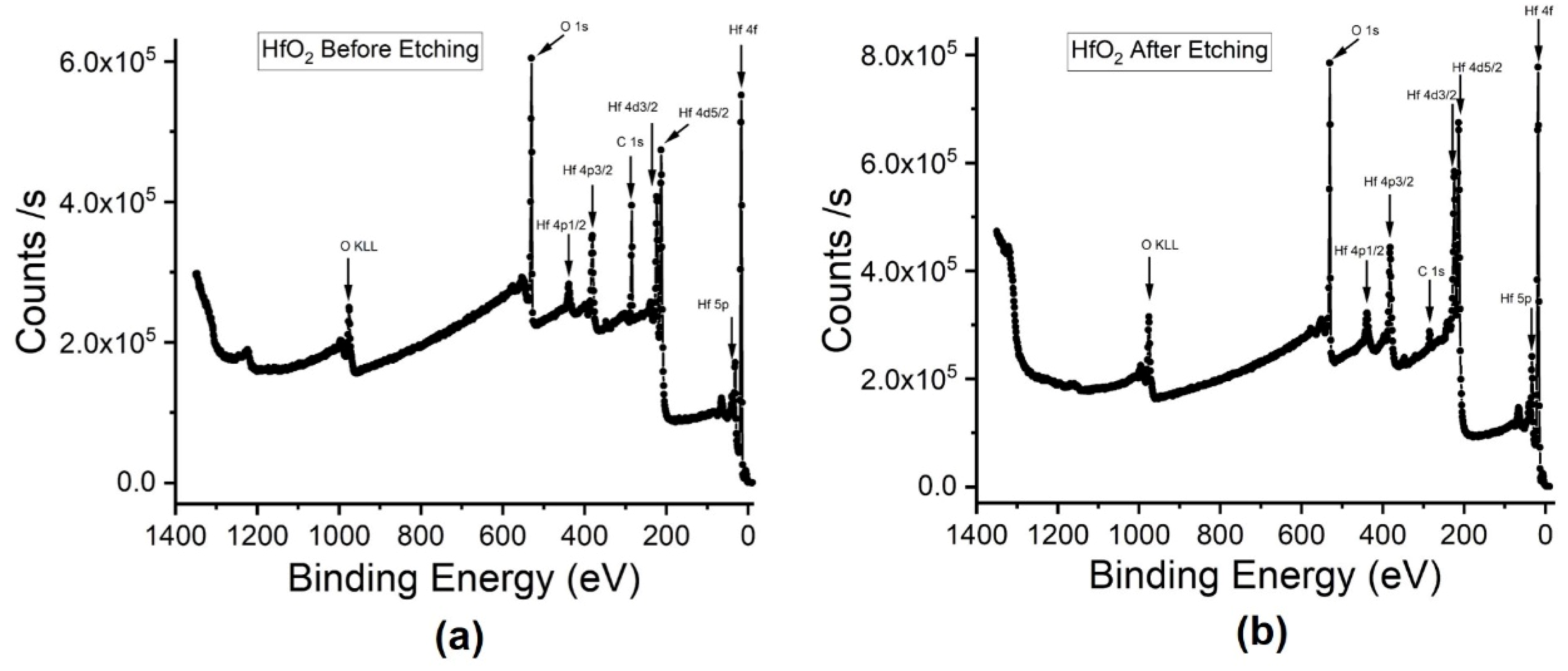
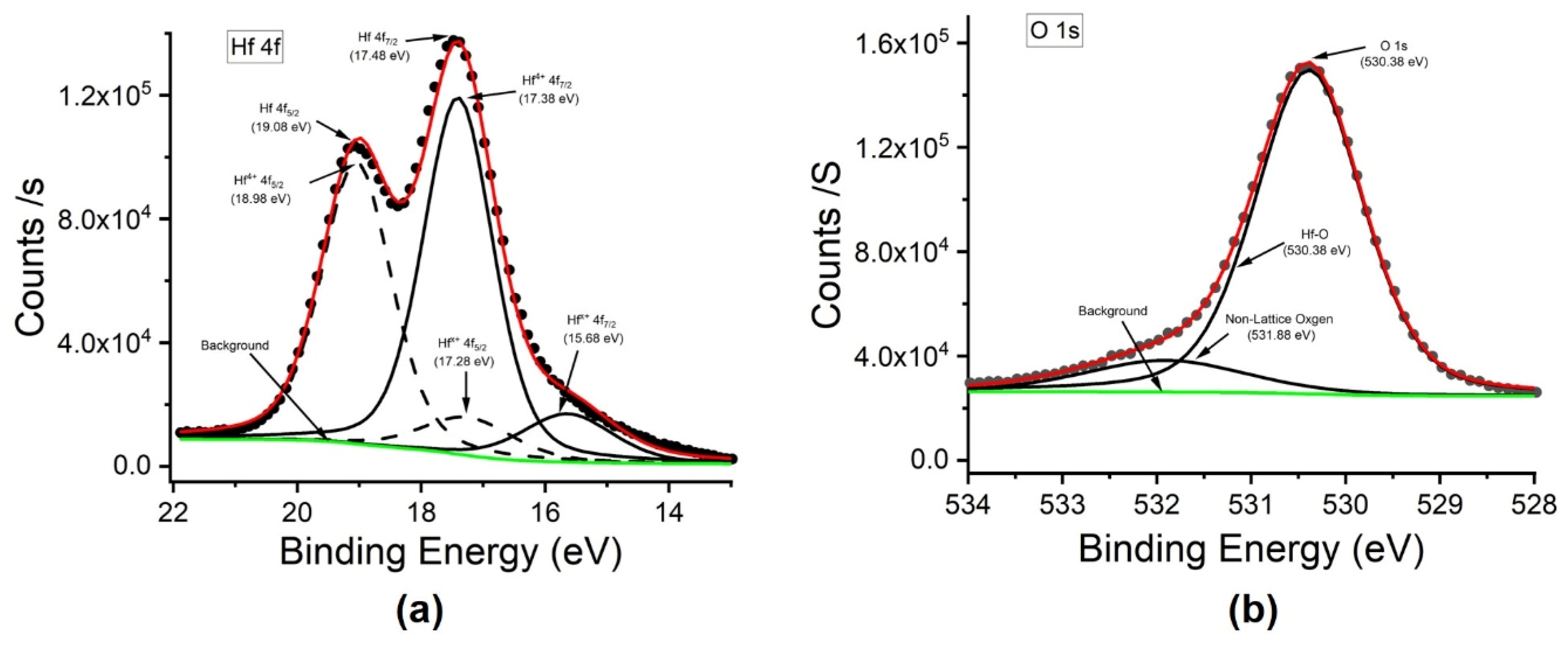
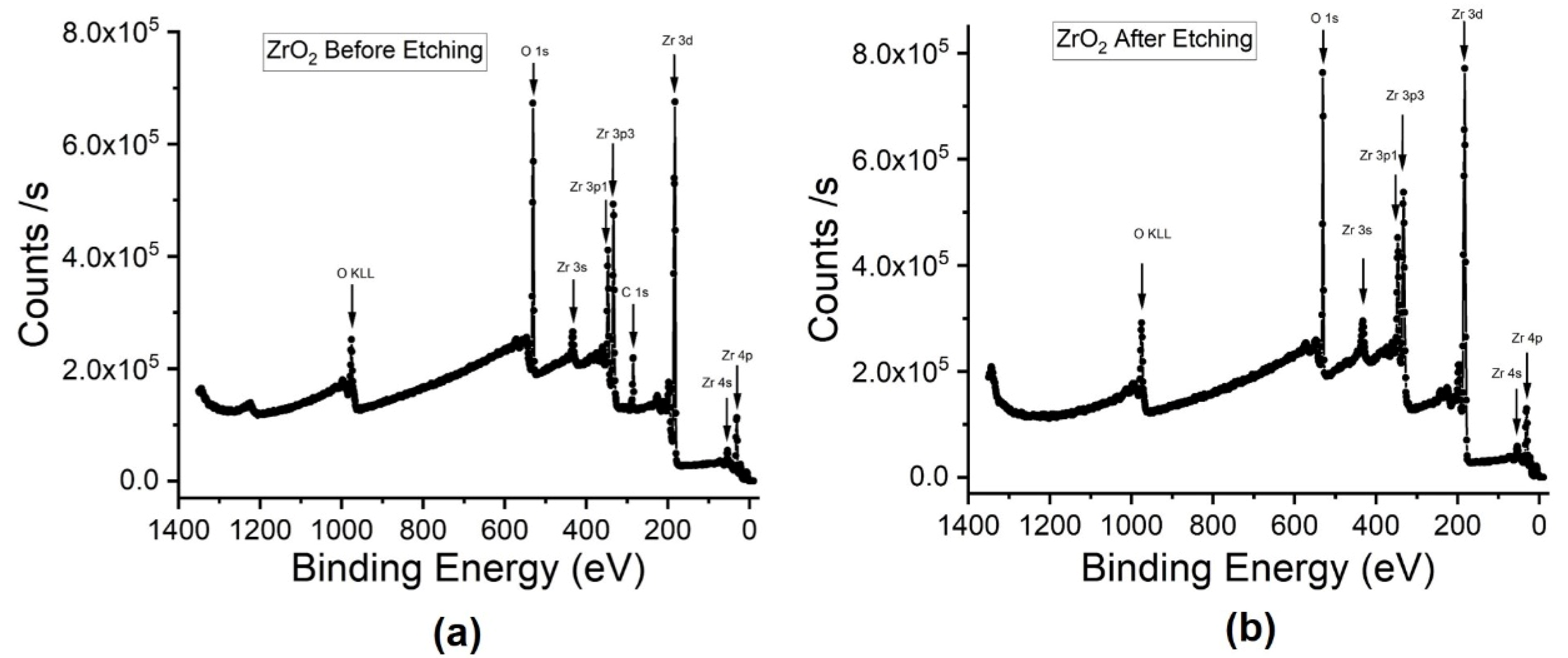
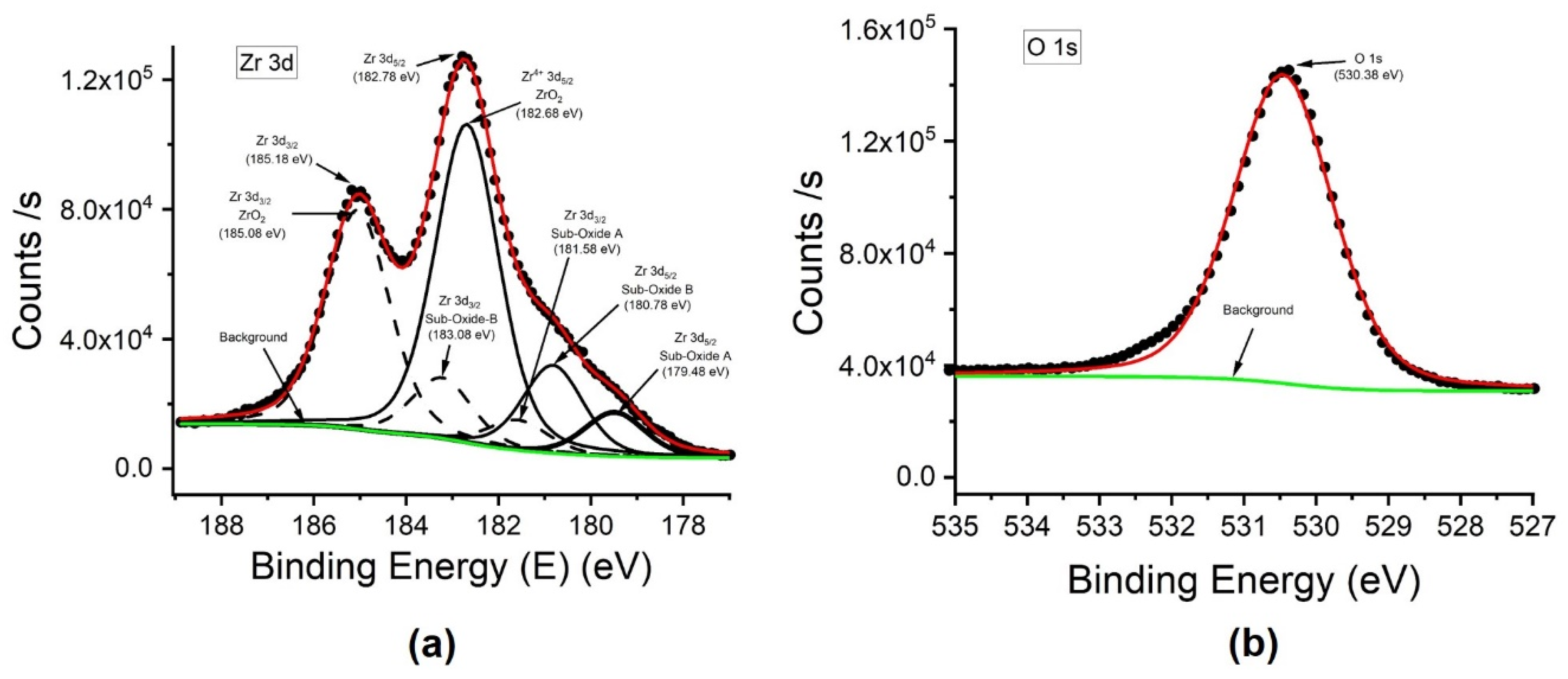
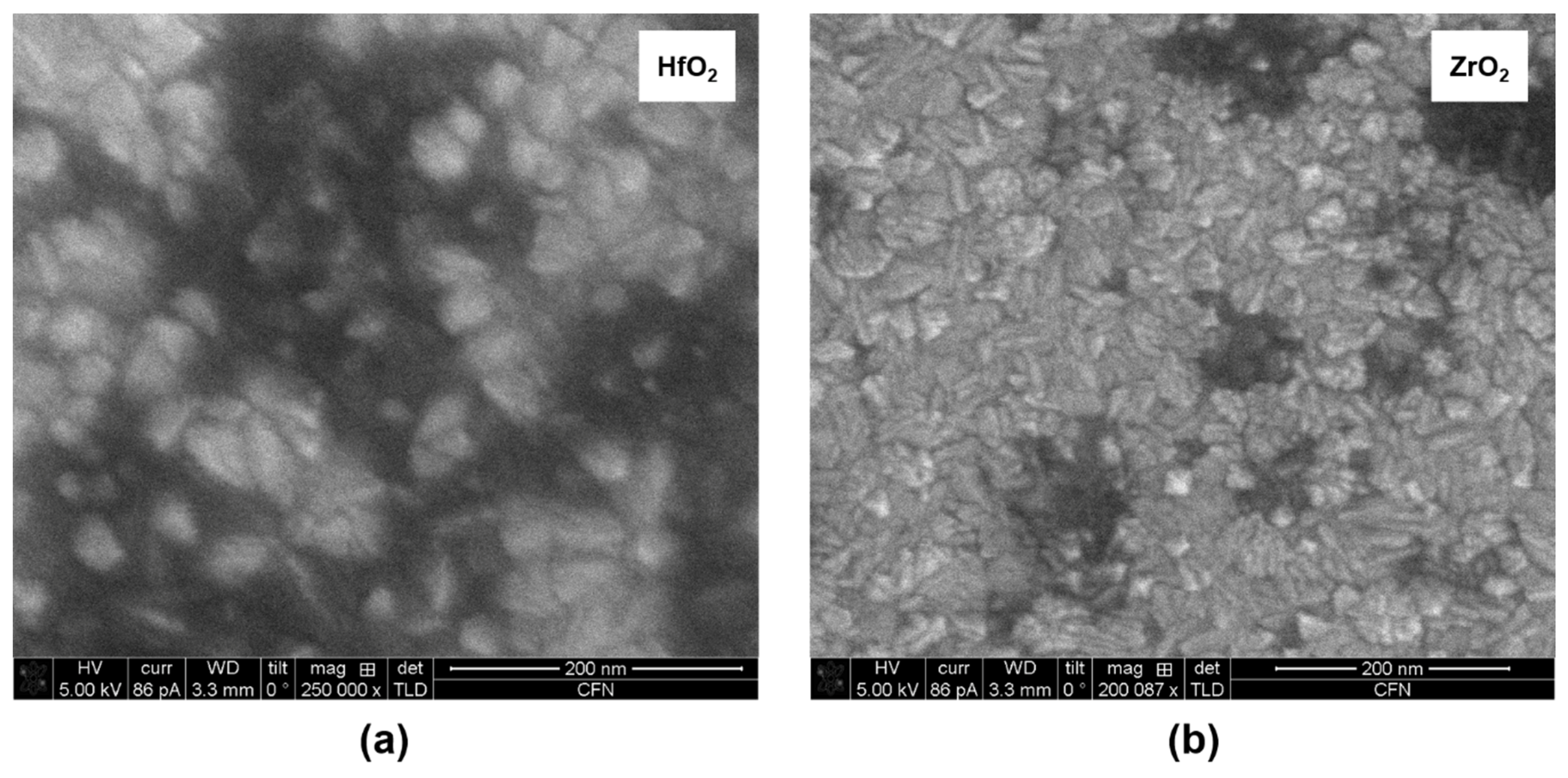
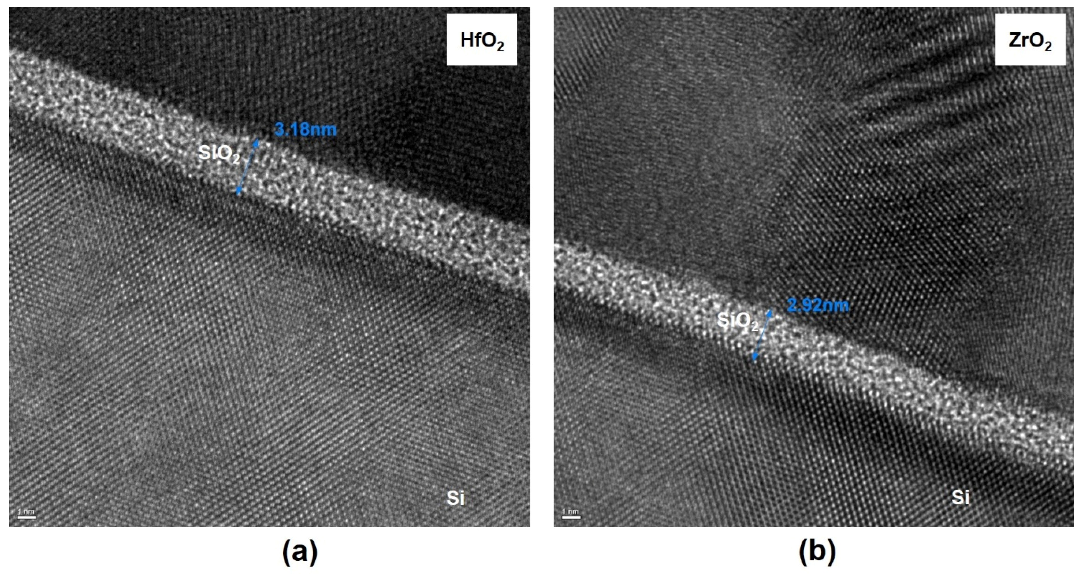
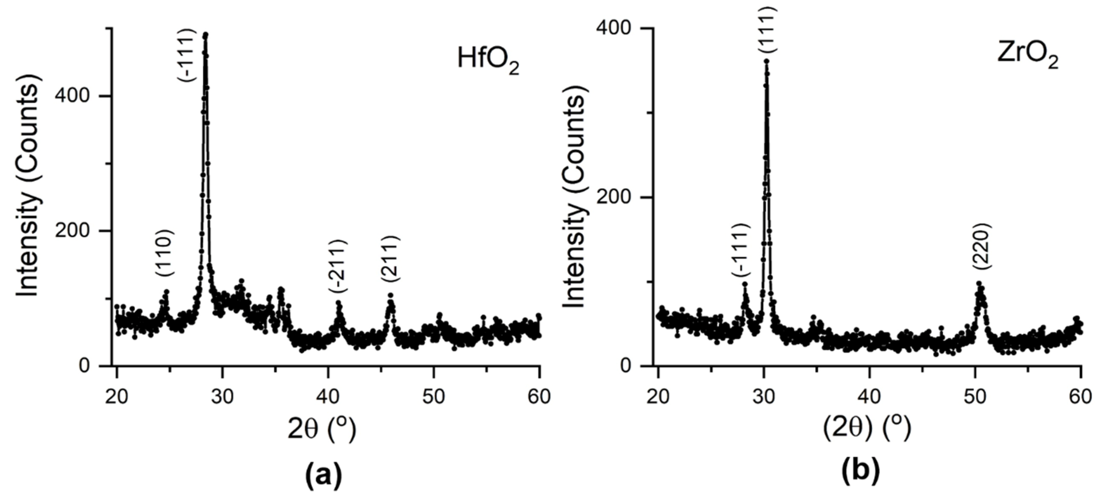
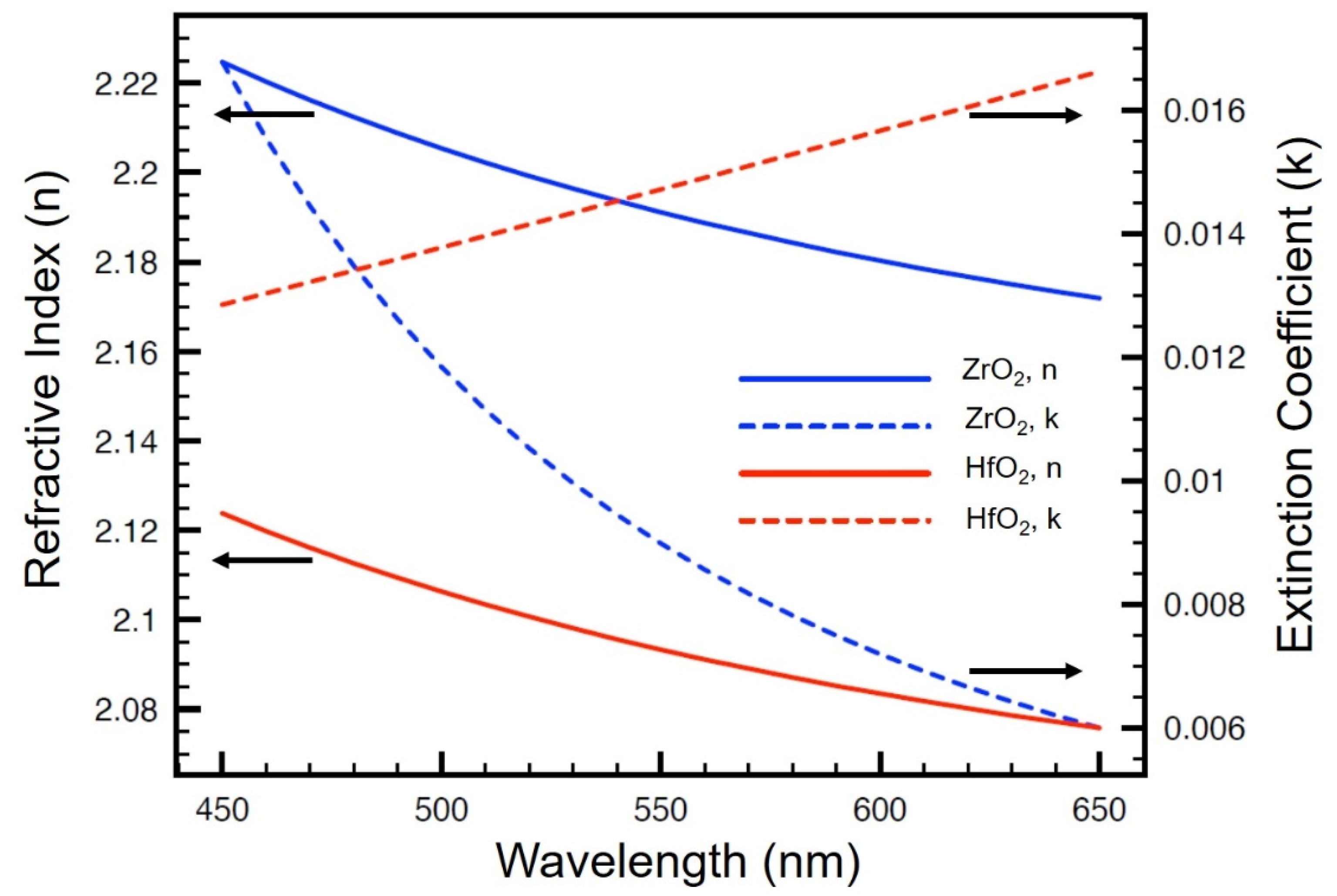
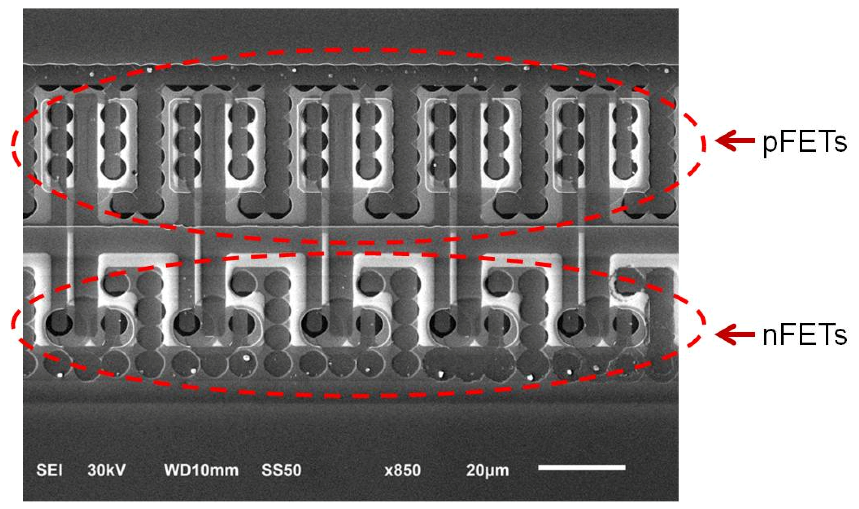
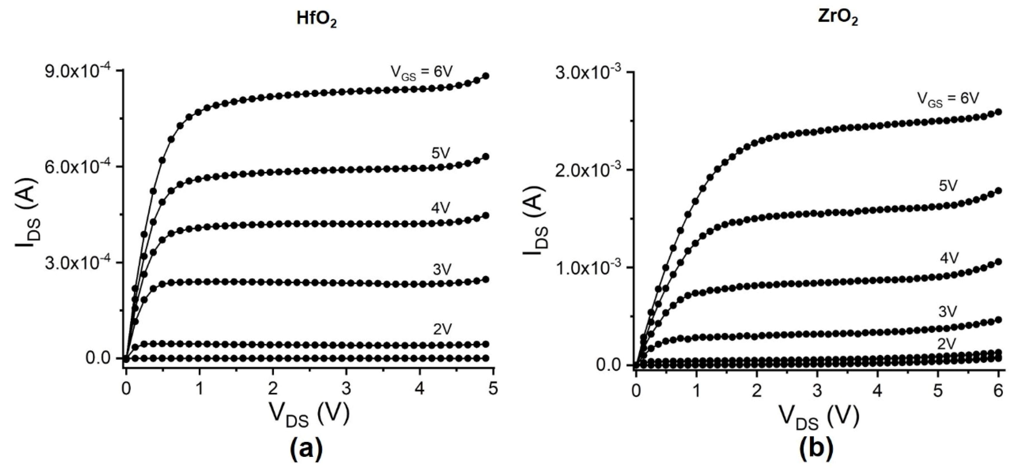
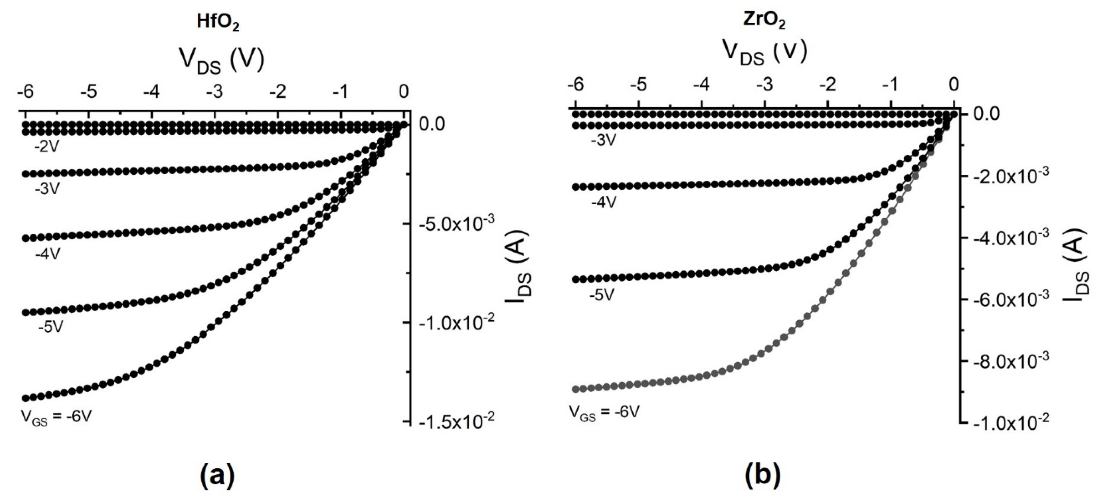
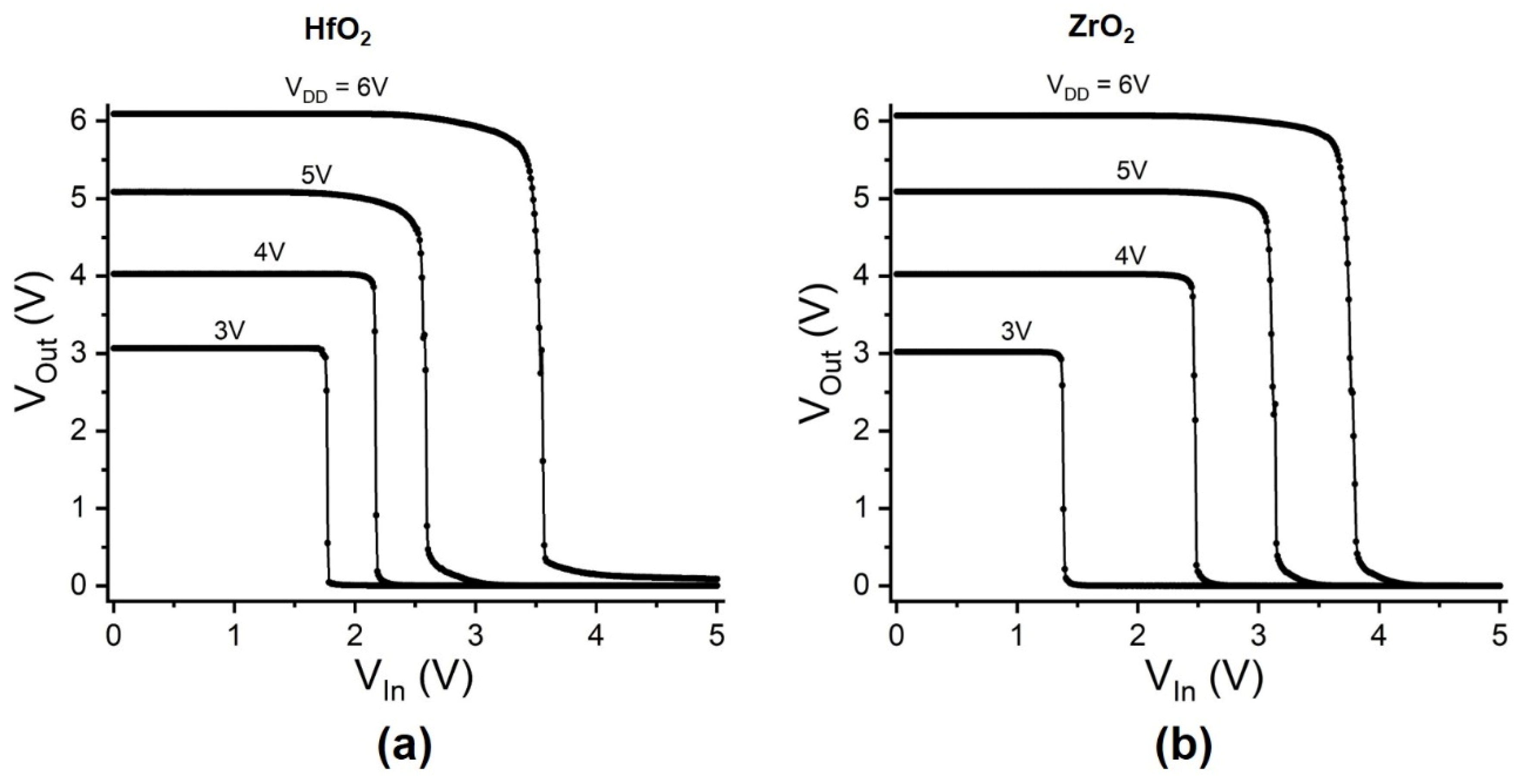
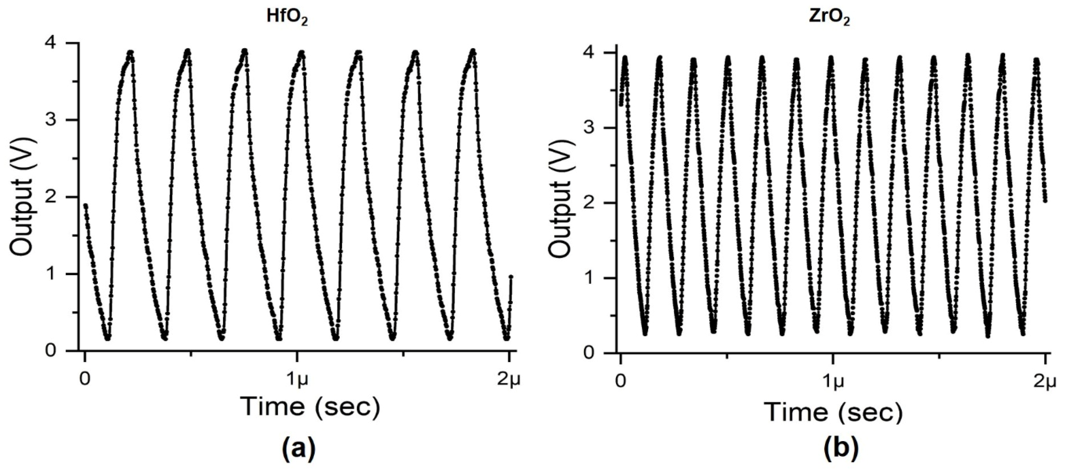
3. Results and Discussion

Table 1 summarizes the compositions and atomic concentrations, which were obtained by the XPS analysis for the HfO2 and ZrO2 thin films grown at the substrate temperature of 270 °C using the remote plasma-enhanced atomic layer deposition. The HfO2 film has the atomic concentrations of 17% Hf, 41% C, and 42% O before etching, and 29% Hf, 11% C, and 60% O after the argon ion etching of film surface for 30 s. The ZrO2 film has the atomic concentrations of 22% Zr, 27% C, and 51% O before etching, and 34% Zr, 2% C, and 64% O after the argon ion etching of film surface for 30 s. The surface of both as-grown HfO2 and ZrO2 films has a higher concentration of carbon, which is due to being exposed to the atmosphere after removal from the growth chamber. Figure 1a,b shows the XPS survey scan of the HfO2 thin film grown at the substrate temperature of 270 °C using the remote plasma-enhanced atomic layer deposition before etching and after etching, respectively. The peak of C 1s after the etching of the film surface is much smaller than that before the etching, which is corresponding to the atomic concentrations before and after the etching in the Table 1. Figure 2a,b show the high-resolution XPS scan of the Hf 4f and O 1 s in the HfO2 thin film, which are compatible with those from the HfO2 film grown by atomic vapor deposition (AVD) [33]. Figure 3a,b show the XPS survey scan of the ZrO2 thin film grown at the substrate temperature of 270 °C using the remote plasma-enhanced atomic layer deposition before etching and after etching, respectively. After etching of the film surface, no peak of C 1s is visible in the XPS scan, indicating that the ZrO2 film has a very low concentration of carbon as shown in the Table 1. The possible reason why the ZrO2 film has a low concentration of carbon is that the precursor of tetrakis (dimethylamino) zirconium (IV) was dissociated well under the argon plasma, making the ZrO2 film fully oxidized. Figure 4a,b show the high-resolution XPS scan of the Zr 3d and O 1s in the Zr O2 thin film. Figure 5a,b show the SEM images of the HfO2 and ZrO2 films. Both HfO2 and ZrO2 films show grain boundaries, while the HfO2 film has a relatively larger grain size than the ZrO2 film. Figure 6a,b show the HRTEM images of the cross section of the HfO2 and ZrO2 thin films grown on single-crystal silicon wafers. Both films show polycrystalline structures [34]. The HRTEM images also show that a silicon dioxide film of about 3 nm thickness was grown on the silicon substrate initially during the growth of both HfO2 and ZrO2 films. Figure 7a,b show the X-ray diffraction (XRD) spectroscopy of the HfO2 and ZrO2 thin films, respectively. The XRD analysis confirms the polycrystal structures of HfO2 and ZrO2 films shown in the HRTEM images in Figure 6a,b. The HfO2 film has a dominating (−111) crystal orientation [35], while the ZrO2 film has a dominating (111) crystal orientation [36].
Figure 8 shows the diffractive index and extinction coefficient of the HfO2 and ZrO2 films as a function of wavelength. The optical constants for the HfO2 and ZrO2 films are compared in the graph. The diffractive index (n) values for both HfO2 and ZrO2 films decrease with increasing wavelength, while the diffractive index (n) values of ZrO2 film are higher than those of the HfO2 film. The n values are comparable with those reported by other researchers [35,36,37,38]. The extinction coefficient (k) values are quite low (<0.02) for both films. However, the “k” curve for the HfO2 film is increasing with increasing wavelength, which is indicative of metallic absorption, which in turn could suggest that the HfO2 may not be fully oxidized as shown in the XPS analysis, and that the HfO2 film has a significant content of carbon. The k curve for HfO2 film is comparable with that reported in Ref. [39]. The “k” curve for the ZrO2 increases with decreasing wavelength, which is more typical of defect-induced (Urbach) absorption in dielectric films and is comparable with those reported in Ref. [40].
Figure 9 shows a SEM image of a 5-stage CMOS ring oscillator fabricated with the HfO2 or ZrO2 as the gate oxide. The ring oscillator consists of 5 CMOS inverters, wherein each inverter consists of an nFET and a pFET. Figure 10a,b present the drain-source current (IDS) as a function of the drain-source voltage (VDS) and gate voltage (VGS) for the nFET (L = 2 µm; W = 6 µm) fabricated with HfO2 and ZrO2 as the gate oxide, respectively. Figure 11a,b present the drain-source current (IDS) as a function of the drain-source voltage (VDS) and gate voltage (VGS) for the pFET (L = 2 µm; W = 18 µm) with HfO2 and ZrO2 as the gate oxide, respectively. Both the nFET and pFET displayed excellent electrical properties of FETs. Figure 12a,b present the electrical transfer characteristics of a CMOS inverter, which consists of an nFET and a pFET fabricated with HfO2 and ZrO2 as the gate oxide, respectively. The applied (VDD (Voltage Drain Drain)) voltages in the measurement are 3 V, 4 V, 5 V, and 6 V. The output voltage decreases sharply from a high voltage (VDD voltage) to a low voltage (GND voltage = 0 V) for all the four cases (VDD = 3 V, 4 V, 5 V and 6 V), while the input voltage increases to the inverting voltage, indicating that the HfO2-based and ZrO2-based CMOS inverters have excellent electrical transfer characteristics and both pFET and nFET in the CMOS inverters functioned very well.
Figure 13a,b illustrate the oscillation waveforms measured at a VDD voltage of 4 V from the CMOS ring oscillators, which were fabricated with HfO2 and ZrO2 as the gate oxide, respectively. Both oscillators produce very good rail-to-rail waveforms, following the VDD voltage (4 V) and the GND voltage (0 V). The oscillator with HfO2 as the gate oxide has a frequency of 3.8 MHz at the VDD voltage of 4 V, while the oscillator with ZrO2 as the gate oxide has a frequency of 6.2 MHz at the VDD voltage of 4 V. The ZrO2 gate oxide makes the oscillator oscillate faster than the HfO2 gate oxide. One possible reason is that ZrO2 has a higher dielectric constant (εr) value (εr = k2) than HfO2 as shown in Figure 8, and higher dielectric constant values made the transistor switch on and off faster. Another possible reason is that the HfO2 film is not fully oxidized and has a significant content of carbon as shown in Table 1, which may degrade the performance and functionality as the gate oxide.

4. Summary

Hafnium dioxide (HfO2) and zirconium dioxide (ZrO2) thin films were grown at a low substrate temperature (270 °C) for the application of electronic materials using the remote plasma-enhanced atomic layer deposition (PE-ALD) method. MOSFETs, CMOS inverters, and CMOS ring oscillators were fabricated with the HfO2 and ZrO2 thin films as the gate oxide. The HfO2 and ZrO2 thin films were analyzed by X-ray photoelectron spectroscopy (XPS), high-resolution transmission electron microscopy (HRTEM), and X-ray diffraction (XRD), revealing stoichiometric compositions, polycrystalline structures, and good interface with silicon. The nFTTs and pFETs fabricated with the HfO2 and ZrO2 thin films as the gate oxide present good current (I)–voltage (V) electrical properties of n-type or p-type field-effect transistors, while the HfO2- and ZrO2-based CMOS inverters present good electrical transfer characteristics of inverters. Both the ring oscillators fabricated with the HfO2 and ZrO2 thin films as the gate oxide demonstrated satisfactory oscillation waveforms, and the ZrO2 gate oxide made the oscillator oscillate faster than the HfO2 gate oxide. The experimental results measured from the HfO2 and ZrO2 films were compared.

Author Contributions

Z.X. designed the experiments, fabricated the materials and devices, measured the electrical properties of the devices, and wrote the manuscript. K.K. performed the HRTEM experiment and contributed to writing the manuscript. S.C. performed the fabrication and characterization of the devices. S.B. performed the fabrication and characterization of the devices. All authors have read and agreed to the published version of the manuscript.

Funding

This research was supported by U.S. Department of Energy, Office of Basic Energy Sciences, under Contract No. DE-SC00112704; National Science Foundation under Grant No. CBET-1740687; and Department of Defense under Grant No. W911NF-16-1-0554 and W911NF-17-1-0474.

Acknowledgments

Research carried out in part at the Center for Functional Nanomaterials, Brookhaven National Laboratory, which is supported by the U.S. Department of Energy, Office of Basic Energy Sciences, under Contract No. DE-SC00112704; the research is supported by National Science Foundation under Grant No. CBET-1740687 and Department of Defense under Grant No. W911NF-16-1-0554 and W911NF-17-1-0474. The authors gratefully thank Dmytro Nytypanchuk at Brookhaven National Laboratory for help in obtaining the XRD analysis, Fernando Camino at Brookhaven National Laboratory for help in obtaining the SEM pictures, Erin C. Prowett at Georgia Institute of Technology for help in obtaining the XPS measurements and analysis, and Blaine Johs in Film Sense LLC for help in analyzing the refractive index and extinction coefficient of the HfO2 and ZrO2 thin films and explaining the data.

Conflicts of Interest

The authors declared no conflict of interest.

References

  1. Wong, H.-S.P. Beyond the conventional transistor. IBM J. Res. Dev. 2002, 46, 133–168. [Google Scholar] [CrossRef]
  2. Robertson, J. High dielectric constant gate oxides for metal oxide Si transistors. Rep. Prog. Phys. 2006, 69, 327–396. [Google Scholar] [CrossRef]
  3. Robertson, J.; Wallace, R.M. High-K materials and metal gates for CMOS applications. Mater. Sci. Eng. 2005, R88, 1–41. [Google Scholar] [CrossRef] [Green Version]
  4. Al-Kuhaili, M.F.; Durrani, S.M.A.; Khawaja, E.E. Characterization of hafnium oxide thin films prepared by electron beam evaporation. J. Phys. D Appl. Phys. 2004, 37, 1254–1261. [Google Scholar] [CrossRef]
  5. Smith, R.C.; Ma, T.; Hoilien, N.; Tsung, L.Y.; Bevan, M.J.; Colombo, L.; Roberts, J.; Campbell, S.A.; Gladfelter, W.L. Chemical vapour deposition of the oxides of titanium, zirconium and hafnium for use as high-k materials in microelectronic devices. A carbon-free precursor for the synthesis of hafnium dioxide. Adv. Mater. Opt. Electron. 2000, 10, 105–114. [Google Scholar] [CrossRef]
  6. Lee, U.S.; Choi, J.S.; Yang, B.S.; Oh, S.; Kim, Y.J.; Oh, M.S.; Heo, J.; Kima, H.J. Formation of a bilayer of ALD-SiO2 and sputtered Al2O3/ZrO2 films on polyethylene terephthalate substrates as a moisture barrier. ECS Solid State Lett. 2013, 2, R13–R15. [Google Scholar]
  7. Venkataraj, S.; Kappertz, O.; Weis, H.; Drese, R.; Jayavel, R.; Wuttig, M. Structural and optical properties of thin zirconium oxide films prepared by reactive direct current magnetron sputtering. J. Appl. Phys. 2002, 92, 3599–3607. [Google Scholar] [CrossRef]
  8. Chang, J.P.; Lin, Y.S.; Chu, K. Rapid thermal chemical vapor deposition of zirconium oxide for metal-oxide semiconductor field effect transistor application. J. Vac. Sci. Technol. B 2001, 19, 1782–1787. [Google Scholar] [CrossRef]
  9. Nienow, A.M.; Roberts, J.T. Chemical vapor deposition of zirconium oxide on aerosolized silicon nanoparticles. Chem. Mater. 2006, 18, 5571–5577. [Google Scholar] [CrossRef]
  10. Choi, K.J.; Shin, W.C.; Yoon, S.G. Ultrathin HfO2 gate dielectric grown by plasma-enhanced chemical vapor deposition using Hf [OC (CH3)3]4 as a precursor in the absence of O2. J. Mater. Res. 2003, 18, 60–65. [Google Scholar] [CrossRef]
  11. Katoa, H.; Nango, T.; Miyagawa, T.; Katagiri, T.; Seol, K.S.; Ohki, Y. Plasma-enhanced chemical vapor deposition and characterization of high-permittivity hafnium and zirconium silicate films. J. Appl. Phys. 2002, 92, 1106–1111. [Google Scholar] [CrossRef]
  12. McNeill, D.W.; Bhattacharya, S.; Wadsworth, H.; Ruddell, F.H.; Mitchell, S.J.N.; Armstrong, B.M.; Gamble, H.S. Atomic layer deposition of hafnium oxide dielectrics on silicon and germanium substrates. J. Mater. Sci. Mater. Electron. 2008, 19, 119. [Google Scholar] [CrossRef]
  13. Senzaki, Y.; Park, S.; Chatham, H.; Bartholomew, L.; Nieveen, W. Physical and electrical characterization of Ce-HfO2 thin films deposited by thermal atomic layer deposition. J. Vac. Sci. Technol. A 2004, 22, 1175–1181. [Google Scholar] [CrossRef]
  14. Hausmann, D.M.; Kim, E.; Becker, J.; Gordon, R.G. Atomic layer deposition of hafnium and zirconium oxides using metal amide precursors. Chem. Mater. 2002, 14, 4350–4358. [Google Scholar] [CrossRef]
  15. Nomura, K.; Ohta, H.; Ueda, K.; Kamiya, T.; Hirano, M.; Hosono, H. Thin-film transistor fabricated in single-crystalline transparent oxide semiconductor. Science 2003, 300, 1269–1272. [Google Scholar] [CrossRef]
  16. Cheynet, M.C.; Pokrant, S.; Tichelaar, F.D.; Rouviere, J.L. Crystal structure and band gap determination of HfO2 thin films. J. Appl. Phys. 2007, 101, 054101–054108. [Google Scholar] [CrossRef] [Green Version]
  17. Bohra, F.; Jiang, B.; Zuo, J.M. Textured crystallization of ultrathin hafnium oxide films on silicon substrate. Appl. Phys. Lett. 2007, 90, 161917. [Google Scholar] [CrossRef]
  18. Kim, H.; Mclntyre, P.C.; Saraswat, K.C. Effects of crystallization on the electrical properties of ultrathin dielectrics grown by atomic layer deposition. Appl. Phys. Lett. 2003, 82, 106–108. [Google Scholar] [CrossRef]
  19. Lao, S.X.; Martin, R.M.; Chang, J.P. Plasma enhanced atomic layer deposition of HfO2 and ZrO2 high-k thin films. J. Vac. Sci. Technol. A 2005, 23, 488–496. [Google Scholar] [CrossRef]
  20. Jung, H.; Oh, I.K.; Yoon, C.M.; Park, B.E.; Lee, S.; Kwon, O.; Lee, W.J.; Kwon, S.H.; Kim, W.H.; Kim, H. Effects of Ar addition to O2 plasma on plasma-enhanced atomic layer deposition of oxide thin films. ACS Appl. Mater. Interfaces 2018, 10, 40286–40293. [Google Scholar] [CrossRef]
  21. Xiao, Z.; Mantei, T.D. Deposition of hard metal nitride-like coatings in an electron cyclotronresonance discharge. Surf. Coat. Technol. 2004, 177, 389–393. [Google Scholar] [CrossRef]
  22. Xiao, Z.; Mantei, T.D. Plasma-assisted growth of bilayer silicon-containing coatings for hardness and corrosion resistance. J. Vac. Sci. Technol. A 2004, 22, 1124–1128. [Google Scholar] [CrossRef]
  23. Xiao, Z. Robust and inexpensive thermal vaporizer for low-vapor pressure liquids. Rev. Sci. Instrum. 2003, 74, 3879–3880. [Google Scholar] [CrossRef]
  24. George, S.M. Atomic layer deposition: An overview. Chem. Rev. 2010, 110, 111–131. [Google Scholar] [CrossRef]
  25. McDaniel, M.D.; Ngo, T.Q.; Hu, S.; Posadas, A.; Demkov, A.A.; Ekerdt, J.G. Atomic layer deposition of perovskite oxides and their epitaxial integration with Si, Ge, and other semiconductors. Appl. Phys. Rev. 2015, 2, 041301. [Google Scholar] [CrossRef]
  26. Motamedi, P.; Cadienn, K. Structural and optical characterization of low-temperature ALD crystalline AlN. J. Cryst. Growth 2015, 421, 45–52. [Google Scholar] [CrossRef]
  27. Johnson, R.W.; Hultqvist, A.; Stacey, F.B. A brief review of atomic layer deposition: From fundamentals to applications. Mater. Today 2014, 17, 236–246. [Google Scholar] [CrossRef]
  28. Profijt, H.B.; Potts, S.E.; van de Sanden, M.C.M.; Kesselsa, W.M.M. Plasma-assisted atomic layer deposition: Basics, opportunities, and challenges. J. Vac. Sci. Technol. A 2011, 29, 050801. [Google Scholar] [CrossRef] [Green Version]
  29. Zhang, Y.; Ren, W.; Jiang, Z.; Yang, S.; Jing, W.; Shi, P.; Wu, X.; Ye, Z.G. Low-temperature remote plasma-enhanced atomic layer deposition of graphene and characterization of its atomic-level structure. J. Mater. Chem. C 2014, 2, 7570–7574. [Google Scholar] [CrossRef]
  30. Huang, R.G.; Tham, D.; Wang, D.; Heath, J.R. High performance ring oscillators from 10-nm wide silicon nanowire field-effect transistors. Nano Res. 2011, 4, 1005–1012. [Google Scholar] [CrossRef]
  31. Wang, H.; Yu, L.; Lee, Y.H.; Shi, Y.; Hsu, A.; Chin, M.L.; Li, L.J.; Dubey, M.; Kong, J.; Palacios, T. Integrated circuits based on bilayer MoS2 transistors. Nano Lett. 2012, 12, 4674–4680. [Google Scholar] [CrossRef] [PubMed] [Green Version]
  32. Xiao, Z.; Kisslinger, K. Electron-beam-evaporated thin films of hafnium dioxide for fabricating electronic devices. J. Vac. Sci. Technol. B 2015, 33, 042001. [Google Scholar] [CrossRef]
  33. Luo, X.; Li, Y.; Yang, H.; Liang, Y.; He, K.; Sun, W.; Lin, H.; Yao, S.; Lu, X.; Wan, L.; et al. Investigation of HfO2 thin films on Si by X-ray photoelectron spectroscopy, Rutherford backscattering, grazing incidence X-ray diffraction and variable angle spectroscopic ellipsometry. Crystals 2018, 8, 248. [Google Scholar] [CrossRef] [Green Version]
  34. Houska, J. Molecular dynamics study of the growth of crystalline ZrO2. Surf. Coat. Technol. 2016, 304, 23–30. [Google Scholar] [CrossRef]
  35. Ramzan, M.; Wasiq, M.F.; Rana, A.M.; Ali, S.; Nadeem, M.Y. Characterization of e-eam evaporated hafnium oxide thin films on post thermal annealing. Appl. Surf. Sci. 2013, 283, 617–622. [Google Scholar] [CrossRef]
  36. Zhao, Z.W.; Tay, B.K.; Huang, L.; Yu, G.Q. Study of the structure and optical properties of nanocrystalline zirconium oxide thin films deposited at low temperatures. J. Phys. D Appl. Phys. 2004, 37, 1701–1705. [Google Scholar] [CrossRef]
  37. Vicek, J.; Belosludtsev, A.; Rezek, J.; Houska, J.; Capek, J.; Cerstvy, R.; Haviar, S. High-rate reactive high-power impulse magnetron sputtering of hard and optically transparent HfO2 films. Surf. Coat. Technol. 2016, 290, 58–64. [Google Scholar]
  38. Vicek, J.; Rezek, J.; Houska, J.; Kozak, T.; Kohout, J. Benefits of the controlled reactive high-power impulse magnetron sputtering of stoichiometric ZrO2 films. Vacuum 2015, 114, 131–141. [Google Scholar]
  39. Ramzan, M.; Rana, A.M.; Ahmed, E.; Wasiq, M.F.; Bhatti, A.S.; Hafeez, M.; Ali, A.; Nadeem, M.Y. Optical characterization of hafnium oxide thin films for heat mirrors. Mater. Sci. Semi. Process. 2015, 32, 22–30. [Google Scholar] [CrossRef]
  40. Sidqi, N.; Clark, C.; Buller, G.S.; Krishna, G.; Thalluri, V.V.; Mitrofanov, J.; Noblet, Y. Comparative study of dielectric coating materials for micro-cavity applications. Opt. Mater. Expr. 2019, 9, 3452–3468. [Google Scholar] [CrossRef]
Figure 1. (a) XPS survey scan of the HfO2 thin film before etching; (b) XPS survey scan of the HfO2 thin film after etching.
Crystals 10 00136 g001
Figure 2. (a) High-resolution XPS scan of the Hf 4f in the HfO2 film; (b) High-resolution XPS scan of the O 1s in the HfO2 film.
Crystals 10 00136 g002
Figure 3. (a) XPS survey scan of the ZrO2 thin film before etching; (b) XPS survey scan of the ZrO2 thin film after etching.
Crystals 10 00136 g003
Figure 4. (a) High-resolution XPS scan of the Zr 3d in the ZrO2 film; (b) High-resolution XPS scan of the O 1s in the ZrO2 film.
Crystals 10 00136 g004
Figure 5. (a) SEM image of the HfO2 thin film; (b) SEM image of the ZrO2 thin film.
Crystals 10 00136 g005
Figure 6. (a) High-resolution transmission electron microscopy (HRTEM) image of the cross section of the HfO2 thin film; (b) HRTEM image of the cross section of the ZrO2 thin film.
Crystals 10 00136 g006
Figure 7. (a) X-ray diffraction (XRD) spectroscopy of the HfO2 thin film; (b) XRD spectroscopy of the ZrO2 thin film.
Crystals 10 00136 g007
Figure 8. Refractive index and extinction coefficient of the HfO2 and ZrO2 thin films versus wavelength.
Crystals 10 00136 g008
Figure 9. SEM image of a complementary metal-oxide semiconductor (CMOS) ring oscillator fabricated with HfO2 or ZrO2 as the gate oxide.
Crystals 10 00136 g009
Figure 10. (a) Drain-source current (IDS) versus drain-source voltage (VDS) and gate voltage (VGS) for the n-channel field-effect transistors (nFET) fabricated with the HfO2 thin film as the gate oxide; (b) Drain-source current (IDS) versus drain-source voltage (VDS) and gate voltage (VGS) for the nFET fabricated with the ZrO2 thin film as the gate oxide.
Crystals 10 00136 g010
Figure 11. (a) Drain-source current (IDS) versus drain-source voltage (VDS) and gate voltage (VGS) for the p-channel field-effect transistors (pFET) fabricated with the HfO2 thin film as the gate oxide; (b) Drain-source current (IDS) versus drain-source voltage (VDS) and gate voltage (VGS) for the pFET fabricated with the ZrO2 thin film as the gate oxide.
Crystals 10 00136 g011
Figure 12. (a) Transfer characteristics of the CMOS inverter fabricated with the HfO2 thin film as the gate oxide; (b) Transfer characteristics of the CMOS inverter fabricated with the ZrO2 thin film as the gate oxide.
Crystals 10 00136 g012
Figure 13. (a) The oscillation waveform of the HfO2-based CMOS ring oscillator at the voltage drain drain (VDD) supply voltage of 4 V; (b) The oscillation waveform of the ZrO2-based CMOS ring oscillator at the VDD voltage of 4 V.
Crystals 10 00136 g013
Table 1. Compositions of HfO2 and ZrO2 films measured by X-ray photoelectron spectroscopy (XPS) before and after etching.
Atomic Concentration (%) of
HfO2 Film
Atomic Concentration (%) of
ZrO2 Film
HfCOZrCO
Before Etching174142222751
After Etching29116034264

