Article

In-Situ Preparation of GaN Sacrificial Layers on Sapphire Substrate in MOVPE Reactor for Self-Separation of the Overgrown GaN Crystal

1
Department Materials, Fraunhofer Institute for Integrated Systems and Device Technology (IISB), Schottkystr. 10, 91058 Erlangen, Germany
2
Chair of Electron Devices, Friedrich-Alexander University Erlangen-Nuremberg, Cauerstr. 6, 91058 Erlangen, Germany
*
Author to whom correspondence should be addressed.
Crystals 2020, 10(12), 1100; https://doi.org/10.3390/cryst10121100
Submission received: 12 October 2020 / Revised: 17 November 2020 / Accepted: 26 November 2020 / Published: 30 November 2020

Abstract

:
GaN layers on sapphire substrates were prepared by using metal organic vapor phase epitaxy (MOVPE) combined with an in-situ H 2 etching process for the purpose of later self-separation of thick GaN crystals produced by hydride vapor phase epitaxy (HVPE) on such substrates. The etching process results in deep pits and long voids that formed on the surface and along the lower interface between GaN and sapphire, respectively. The pits, which were investigated by SEM analysis, can be modified in their aspect ratio and density by controlling the etching parameters. Using a proper set of in-situ etching parameters, a seed layer with internal voids can be prepared, which is suitable for HVPE overgrowth and the self-separation process. The quality of the in-situ-etched seed GaN layer and overgrown GaN crystal were characterized by X-ray diffraction (XRD) and defect selective etching (DSE). With the aid of atomic force microscopy (AFM) in tapping mode, the interface morphology of the separated GaN crystal was analyzed. The crystal quality of the separated HVPE-GaN crystal is comparable to the crystal grown on untreated GaN MOVPE-seed, which did not separate from the sapphire substrate. The introduced technique to promote the crystal separation during the HVPE process has no obvious drawback on the quality of the grown GaN crystals. Using this technique, the self-separation occurs more gently due to a weakened interface between GaN/sapphire. The conventional separation from an untreated seed by pure thermomechanical action results in higher mechanical forces on the crystal and consequently much higher risk of crystal breakage.

1. Introduction

Vertical GaN device architectures have attracted more attention because of their application in high-power and high-frequency electronic devices [1,2,3,4]. However, the commercialization of vertical architectures is strongly hampered because native GaN substrates with good quality and moderate costs are not available. GaN bulk crystals, from which the native GaN substrates are manufactured, are mostly grown by the hydride vapor phase epitaxy (HVPE) process on different kinds of substrates. Sapphire substrates are one of the candidates that are often used. In this case, either the GaN crystal is grown directly on the sapphire substrate in the HVPE reactor, or a GaN epilayer on sapphire is prepared in advance in a metal organic vapor phase epitaxy (MOVPE) reactor and used as a seed for subsequent overgrowth in the HVPE reactor. At this point, the challenge is to remove the sapphire substrate from the HVPE GaN crystal. There are some technologies for an in-situ or ex-situ separation of the GaN crystal from the sapphire substrate, such as mechanical lapping or self-lift-off. Creating a GaN seed layer between the sapphire and the GaN crystal, acting as a weak layer to facilitate the self-lift-off either during growth or during the cooling down process, would reduce the necessary mechanical forces a lot and is sufficient for a successful separation. Weakening the interface between GaN and sapphire was achieved by either patterning the GaN/sapphire interface [5,6] or inserting an in-situ mask [7,8]. The patterning methods require additional lithography steps. Therefore, they are costly and time consuming. For the case of an in-situ mask, an optimization of the mask material (thickness) and the 3D nucleation of GaN deposited on it is required, in order to avoid formation of new defects starting from the mask. Amilusik et al. [8] have shown the importance of nitridation, when using a Ti mask for self-lift-off. Apart from the required optimization of the mask material, this method has been one of the most successful methods so far.
A lift-off without any extra layer of foreign material (e.g., nano mask) could function by thermomechanical action. However, this requires great mechanical forces, which enhance the possibility of crystal breakage. In the thermomechanical self-separation case, a key point is the thickness of the GaN crystal. In this method, a precise stress distribution control is required during GaN heteroepitaxial growth to cause a controllable self-separation. However, achieving such a separation may cause damage to the separation interface, meaning the backside of the GaN crystal. Subsequently, the yield for wafers to be cut out of the crystal is reduced dramatically, even if the crystal does not break.
In this work, we investigated a new type of seed layer preparation for GaN bulk crystal growth, so that a thick GaN crystal can be grown with good crystal quality, while having a modified GaN seed layer beneath, which supports the self-separation. Therefore, we developed a maskless etching technique for the creation of internal voids in a GaN seed layer. This approach would allow a reduction in the cost of production and time of seed preparation. We will show that the structural quality of the overgrown and self-separated GaN HVPE crystal on the seeds is comparable to the HVPE crystals grown on untreated MOVPE seeds. We compare the quality of the separation of the HVPE grown crystal on an in-situ etched seed with a relatively thicker GaN crystal, which we could separate from the sapphire substrate with the stress-induced self-lift-off method. The advantage of the self-separation method by our introduced method over the stress-induced self-lift-off method will be discussed.

2. Materials and Methods

2.1. Principle of GaN Seed Layer Preparation in MOVPE

For better imagination of such an in-situ etching process, a schematic illustration is displayed in Figure 1. A key feature of this etching process is that threading dislocations act as “etch channels” in order to access the GaN/sapphire interface. This can be understood as follows: it was reported that   H 2 , in the absence of   NH 3 , reacts with GaN, mostly at nitrogen-terminated planes and subsequently, H and N atoms combine to form NH 3 at high temperature, which is dissipated from the pits [9,10]. Thereby, the different lattice planes in the GaN epitaxial layer have different stabilities against the H 2 etching action and the degree of stability is reflected by the amount of dangling N-bonds in a certain plane. The most chemically stable lattice plane is the Ga-polar c-plane, followed by the non-polar, inclined and N-polar facets [9]. As threading dislocations are disordered and strained sites have more N-terminated sidewalls, it would be expected that the dislocations are etched preferentially downward to the sapphire/GaN interface. The interface weakening by in-situ etching in MOVPE should be good enough to facilitate the self-lift-off process with moderate forces. Due to the thermal mismatch between GaN/sapphire, strain is built up along the interface between the GaN layer and substrate during the growth of a thick GaN crystal in HVPE [11]. Due to this strain, the GaN crystal separates from the underlying substrate during overgrowth or the cooling down process, if the interface is weakened or the forces are high enough.
The advantage of this method of seed preparation over already introduced methods is first of all the reproducibility and simplicity of the in-situ etching process. Additionally, the in-situ etching process is completed in a short time, only about 5 min, in the MOVPE right after the growth process, meaning no additional complicated and costly processing is needed. The seed does not experience any additional handling, which may avoid issues such as cleaning prior to overgrowth. Finally, yet importantly, the GaN seed layers created by our approach have a smooth surface and good crystal quality.

2.2. Experimental Details

The epitaxial GaN films used for seeding layers were grown in a MOVPE reactor in a close-coupled showerhead configuration on 3 inch c-plane sapphire substrates with a thickness of about 430 µm. As precursors, trimethyl-gallium   ( TMGa ) and ammonia ( NH 3 ) were used, with   H 2 as carrier gas. After the growth of an about 4.8 µm thick GaN layer, NH 3   entered the reactor in order to avoid GaN decomposition until the etching parameters were stable. Then, the NH 3 flow was switched off and   H 2 as etchant gas, diluted in   N 2 , flows into the reactor. As a starting point of the in-situ etching experiments, two identical reference samples, A and A * , were prepared at a temperature of 1150 °C (surface temperature) and a pressure of 130 mbar for a time of 5 min with an etchant gas flow ratio N 2 : H 2 of 5:1. A series of samples with the same nominal GaN layer were prepared under different etching conditions. The etching parameters are compiled in Table 1. The subsequent overgrowth process was carried out in a HVPE reactor along the c-direction of the GaN lattice, applying a growth rate of approximately   85   μ m / h at a temperature of about 950 °C.
The influence of these etching parameters on the surface morphology of the seed layer and on the geometry of the etched pits was analyzed in plan-view and cross-section imaging by scanning electron microscopy (SEM JEOL-6610, JEOL Ltd., Tokyo, Japan).
Atomic force microscopy (AFM, Bruker, Billerica, MA, USA) measurements in tapping mode with a Bruker Dimension Icon tool were completed to determine the topography of the HVPE GaN crystal backside after separation. For evaluation of the crystal quality, X-ray diffraction (XRD) and defect selective etching (DSE) experiments along with SEM imaging were performed. The XRD measurements were carried out in a Panalytical X’Pert PRO MRD (Malvern Panalytical, Kassel, Germany) system equipped with a 4-bounce Ge (220) hybrid monochromator and triple-axis diffractometer. The defect selective etching (DSE) experiments [12] were performed with molten KOH:NaOH at 450 °C, in order to etch the single dislocations. Subsequently, the etch pits were counted from SEM images.

3. Results

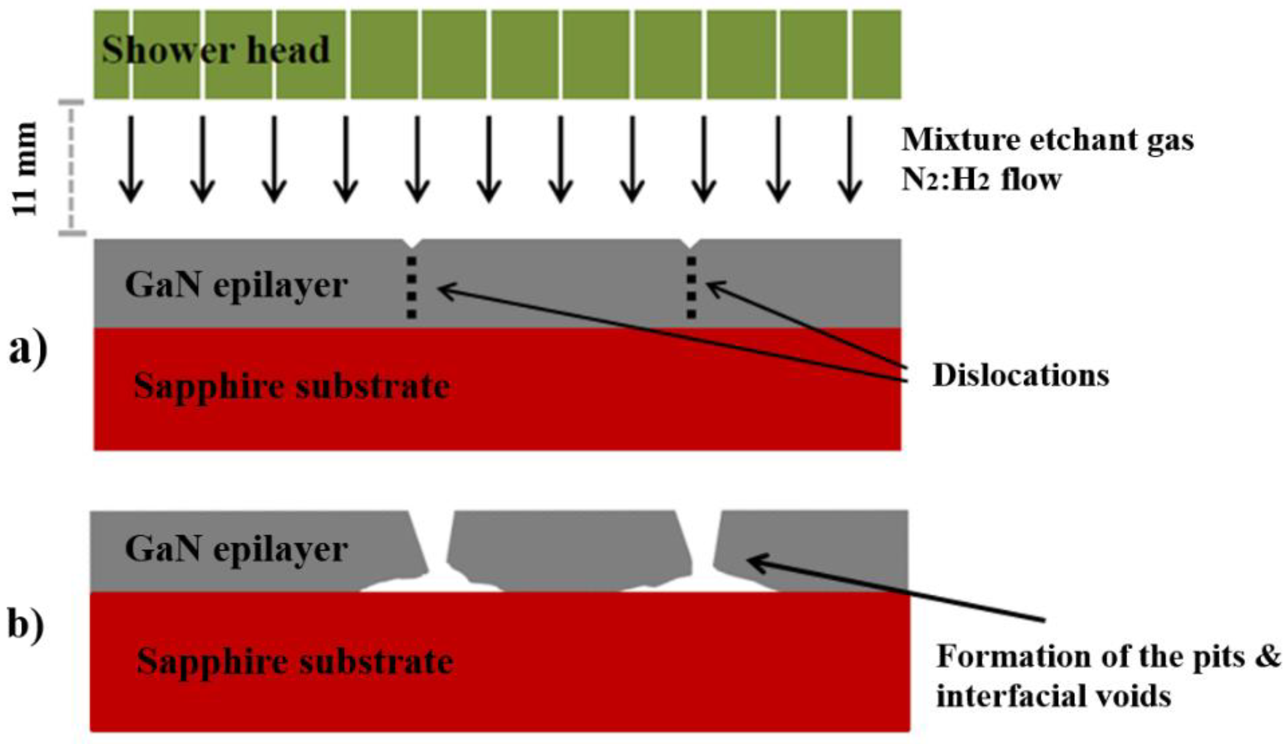
3.1. GaN Seeds Preparation

The SEM cross-sections and plan views of eight in-situ etched samples under different etching conditions are shown in Figure 2 and Figure 3, respectively. As it can be seen in all samples, the GaN surface remains quite smooth after the in-situ etching treatment. The smoothness of the GaN surface refers to the relative stability of the Ga-face against   H 2 etching, as was explained previously. Additionally, etch pits are visible on the samples, which are never present in untreated-GaN layers without an additional etching step. The density and the geometry of the pits depend on the etching parameters, as will be explained in the following sections.
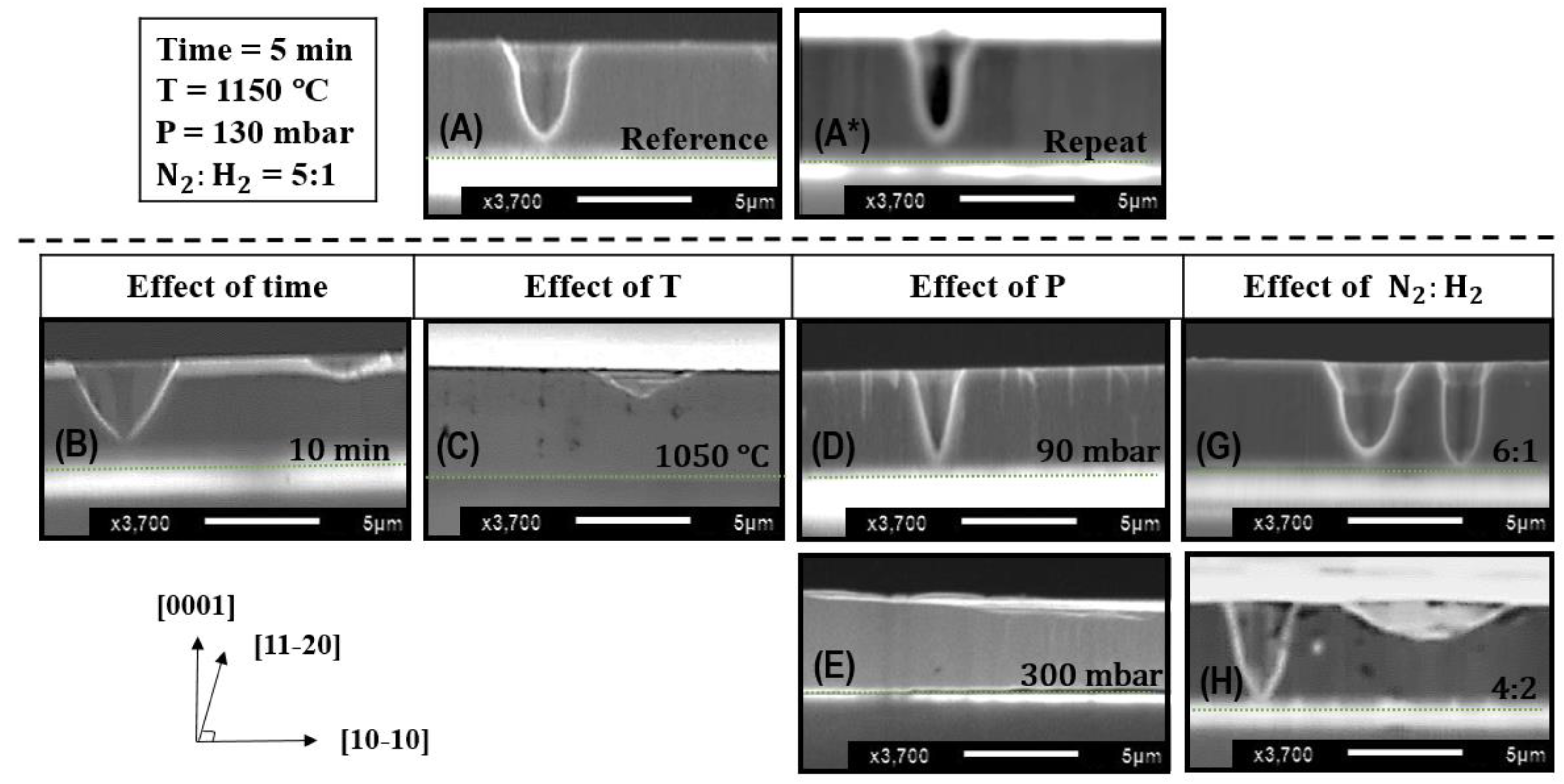
In sample A, the depth of the etch pits is about   4.5   μ m , i.e., the tip of the pits is close to the interface between the GaN layer and the sapphire substrate. The etching procedure is considered reproducible as the density, geometry and relative depth of the pits are almost the same in sample A*, which was etched under the same conditions as sample A. However, a statistical variation in the observation of the exact physical depth should be considered, as the probability of being able to cut the sample exactly in the middle of a pit is low and therefore the depth of the etch pits are generally underestimated. It is worth noting that, since the pits have very steep inclined sidewalls, measuring the depth of them by means of confocal laser microscopy, atomic force microscopy or similar methods was not successful. Hence, the statistics from the SEM cross-section images must be considered as the only reliable method to obtain etch pit depth information.
Since the target was to etch the GaN seed layer in such a way that the etch pits become as close as possible to the GaN/sapphire interface in order to weaken the interface, we have increased the etching time to 10 min for sample B, in order to allow the   H 2 to further diffuse through the dislocations and eventually along the GaN/sapphire interface. It was found that the aspect ratio (diameter/depth) of the pits was increased with etching time, but no increase in the depth of the pits was observed. We conclude that either the GaN layer was etched up to some depth and then   H 2 continued etching the sidewalls of the formed pits laterally (see Figure 2, sample H) so that only the diameter grew bigger. The other possibility would be that the pits are etched up to the interface and with increasing time etched sideward. However, as mentioned, the depth of the pits measured from the cross-sections could be underestimated. In order to prove which one of the above assumptions is valid, we undertook further experiments.
By lowering the temperature, the etching rate decreased notably, achieving a maximum pit depth of about   1   μ m only (see sample C in Figure 2 and Figure 3). This indicates that the etching rate along the c-direction is higher at elevated temperatures. This can be attributed to the higher desorption flux of Ga atoms at higher temperatures, which more likely occurs at less stable crystal facets. Therefore, a higher temperature is suitable for more intense etching along the pits. However, this could only be proven up to the high-end-point temperature of our reactor heater, which was 1300 °C (surface temperature of 1150 °C).
In contrast, if instead the etching pressure was reduced from 130 mbar (sample A) to 90 mbar (sample D), the diameter of the etch pits did not change significantly, but the depth and pit density increased. This result was promising, considering that more volume of GaN is being etched and the pits become comparably closer to the GaN/sapphire interface. By increasing the reactor pressure to 300 mbar (sample E), the etching rate drops dramatically and the picture became inhomogeneous. In some areas of the sample, almost no etching appeared whereas a non-uniform distribution of the pits was observed in other regions of the sample. Obviously, the etching process under such conditions is less anisotropic compared to etching at a relatively low pressure. This can be explained by the smaller mean free path of the atoms and molecules in the gas phase, which is inversely proportional to the pressure at constant temperature. Therefore, low reactor pressure should be more suitable for vertical etching.
In order to further enhance the vertical etching towards the interface, the amount of   H 2 flow was increased by changing the N 2 : H 2 ratio to 4:2 (sample H). As a result, the etch pit density as well as the pit size increased significantly. On the other hand, it is obvious from the plan-view and cross-section SEM images of sample H that the size and depth of the etch pits were not homogenous anymore. Reducing the amount of   H 2   flow by increasing the ratio of   N 2 : H 2   from 5:1 (sample A) and to 6:1 (sample G) does not change the etch pit depth, but reduces the density of the pits, because the etchant gas is diluted by more   N 2 , which results in less etching.
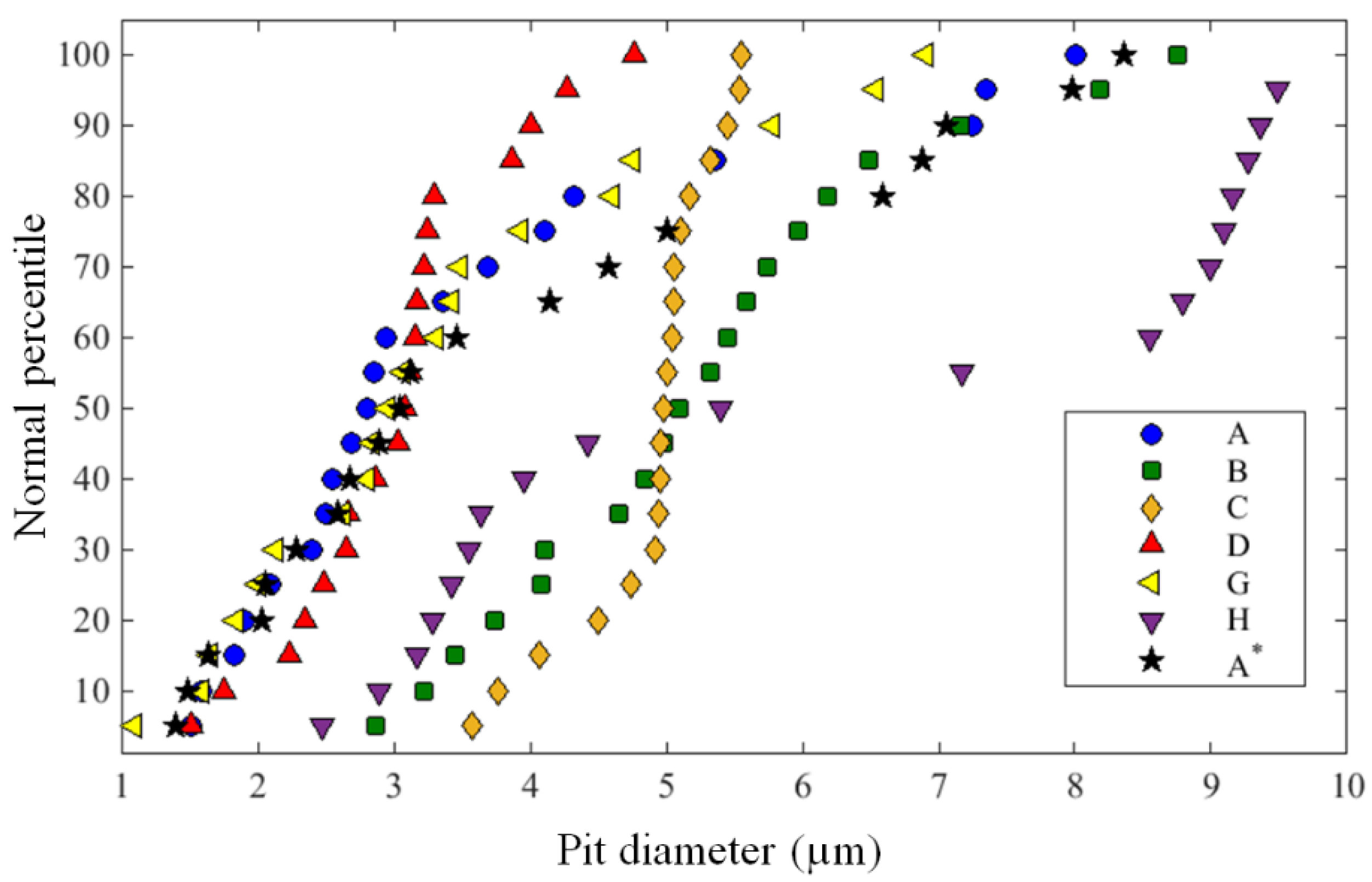
We assume that for a uniform separation of a larger diameter crystal, a uniform size and distribution of pits over the whole sample are required. Therefore, based on the results from the plan-view images, we have statistically analyzed the size and density of the pits on the GaN surfaces etched under different conditions. For this purpose, SEM images with an area of about 250 × 170 µm2 from three positions radially from the center to the edge of the samples were analyzed. Two representative SEM images from samples A and A* in a large scale for comparison of the etch pit density and distribution along with a plot of summarized results are shown in Figure 4. On all samples, the density of the pits is in the same order of magnitude, i.e., in the range of   0.5 × 10 5   to   4 × 10 5   cm 2 , and the diameter of the pits varies from 1 to 10 µm. It is worth mentioning that the density of the pits formed at the surface is some orders of magnitude less than the typically expected dislocation density of a MOVPE GaN layer, which is usually 6 × 10 8   to   8 × 10 8   cm 2 in our samples, meaning that not all present dislocations were etched to form pits. However, this topic will not be discussed further in this paper.
The diameters of the pits, which were measured out of the SEM images, are plotted in Figure 5 for a better comparison of the average size and homogeneity of the etch pits. In principle, a narrow distribution of the etch pit diameter over the full wafer is required. In Figure 5, one can see the largest inhomogeneity of the size distribution of the etch pits for sample H, with etch pits with diameters from about 2 to 10 µm. As mentioned before, such an inhomogeneity could cause a non-uniformity of the overgrown crystal and consequently influence the separation process. The large etch pits can easily be filled during overgrowth in the HVPE reactor. Therefore, this sample is not well suited for a subsequent overgrowth process. The best samples regarding uniform etch pit diameter are samples C and D with etch pits in the size of 3.5–5.5 µm and 1.5–4.5 µm, respectively. However, the density of the etch pits in sample C is lower than in sample D (see Figure 4). This means that, in case of sample C, less voids would exist at the GaN/sapphire interface in comparison to sample D, helping the self-lift-off process.
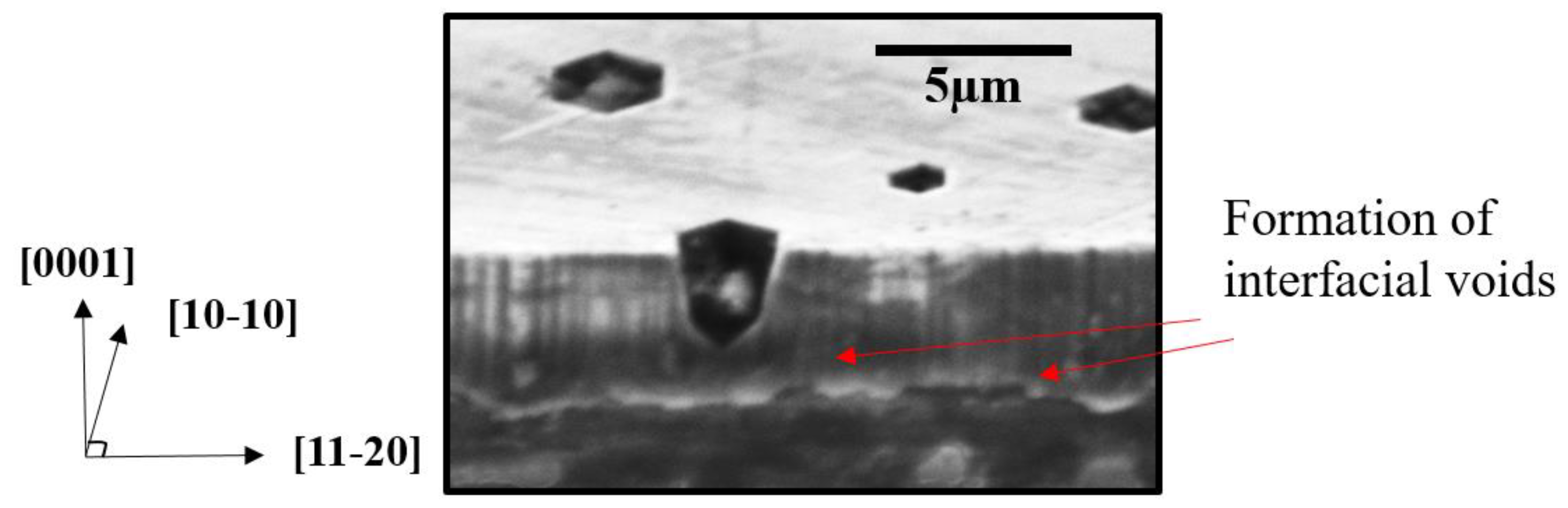
Summarizing the results shown above, we defined a set of criteria for the selection of an appropriate seed: the GaN layer should have relatively deep pits (as close as possible to the interface) with an extension of voids along the GaN/sapphire interface, uniformly distributed over the whole sample, in high density with moderate diameters (smaller than about 5 µm). In the ideal case, they would not be completely filled up during the HVPE overgrowth in order to remain as voids supporting the separation. However, whether they are being filled or not during the first growth stage in the HVPE process would not only depend on the etching procedure, but also on the parameters of the HVPE process itself. If a pit were too wide, it could mean that it will possibly not close during overgrowth and the result would be growth disturbances and an uneven growth front with macro defects. Alternatively, for wider pits, the probability is higher that the pit would be filled completely during the HVPE process and no voids remain—facilitating the separation process. However, irrespective of whether the pits would be filled or not, the lateral voids along the interface would act as a separation support feature. Taken all the above discussed issues into account, we conclude that the etching conditions for sample D are best-suited to prepare a seed for overgrowth in the HVPE process: the density of the pits is relatively high (3 × 105 cm−2), the pits have an average depth of 4.6 µm and a narrow diameter range of 1.5–4.5 µm, and they are uniformly distributed over the whole sample. This is also underlined by further SEM investigations on sample D, in which one could clearly observe the formation of the interfacial voids, as shown in Figure 6. These interfacial voids are very thin; therefore, they are not easily resolvable in standard SEM cross-section images. Thus, they cannot be seen in Figure 2.

3.2. HVPE Overgrowth Process and Results

An in-situ etched seed prepared by the etching conditions of sample D was overgrown, applying a standard HVPE process suited for the growth of thicker layers of several 100 µm thickness or even bulk crystals. The 3 inch GaN crystal separated itself very smoothly from the substrate during the HVPE process at a thickness of about   400   μ m . It is worth noting that GaN crystals grown on untreated seeds usually remain attached to the sapphire substrate at such thickness values. The separated GaN crystal had some cracks close to the edge of the crystal. This could be the case because up to 1 mm away from the edge of sapphire substrate, a polycrystalline GaN growth occurred. This rim area also behaved differently during the seed preparation step by in-situ   H 2 etching in the MOVPE reactor. Therefore, this area could affect the separation process. However, there are several options to overcome this problem, (i) optimize the etching process and ensure that the seed would be etched until the outer edges or (ii) optimize the HVPE GaN growth with regard to thickness homogeneity and better adapt the nucleation regime during HVPE to the new seed type.
Comparing the backside of the separated GaN crystal (about 400 µm) with an in-situ etched seed underneath to a GaN crystal that was separated from sapphire at a thickness of about 1.5 mm by stress-induced spontaneous self-lift-off shows a big difference. The difference can be seen in the microscopical images in Figure 7 taken with a stereomicroscope.
On the backside of the latter crystals, we always observed huge grooves with depths from hundreds of micrometers up to some millimeters, as seen in Figure 7b, while the separation from in-situ etched seeds occurs very gently, leaving a smooth crystal backside, as shown in Figure 7a. The grooves are formed because the mechanical forces to tear the crystal off the seed are very high. Moreover, such a strong thermomechanical action may additionally cause the formation of micro cracks in the crystal.
AFM images from the backside (separated interface) of the GaN crystal are shown in Figure 8, along with a schematic indicating where the measurements were carried out. In the AFM images from the separated interface, one can clearly see the interfacial voids, which were initially generated by the in-situ etching of the seed. These voids have therefore likely caused the smooth separation of the crystal from the sapphire substrate. The depth of the depressions or voids is about 50 nm. This observation is very promising and proves that the GaN/sapphire interface was etched very nicely and weakened in a very thin layer.
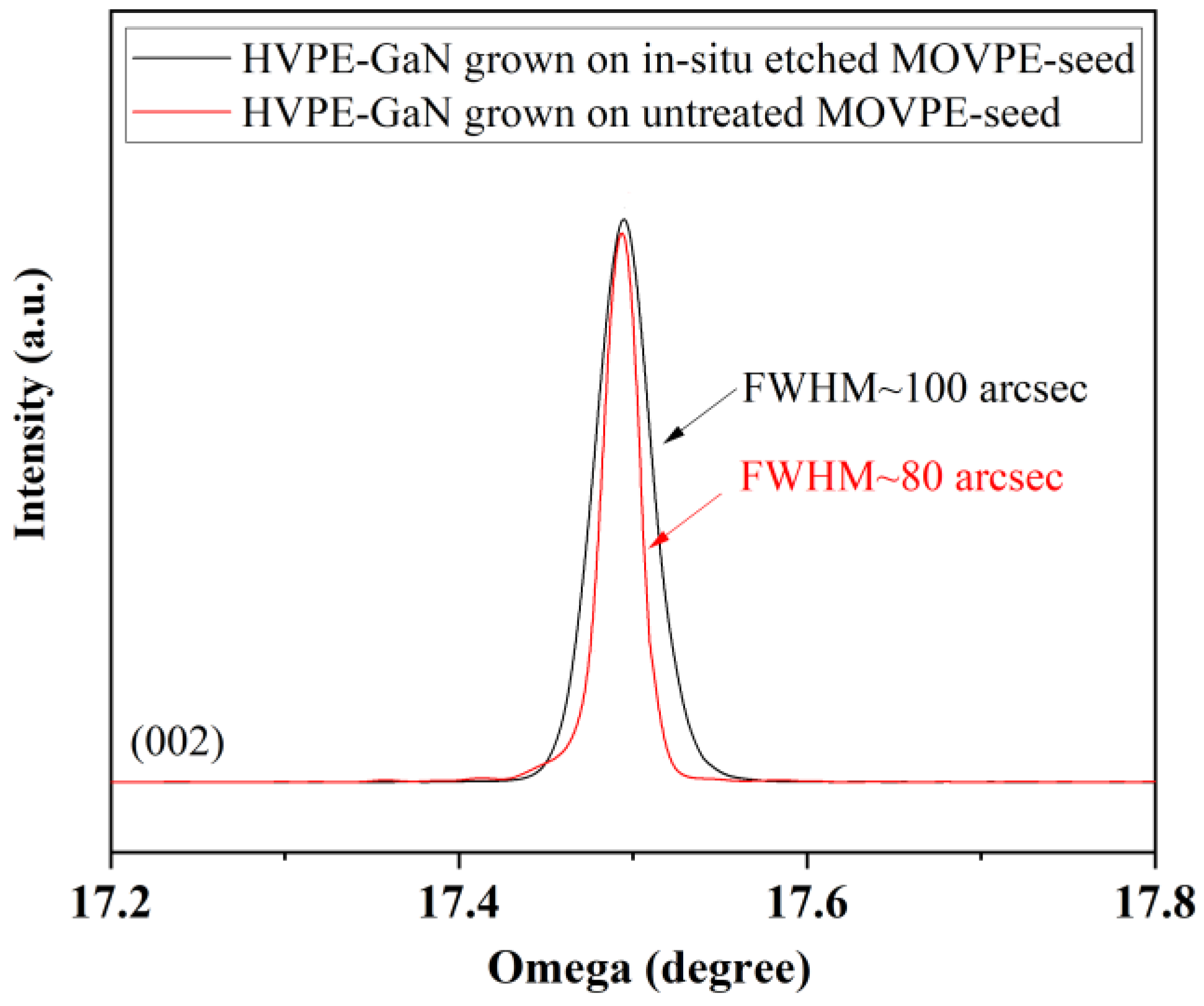
We investigated the crystal quality of the HVPE GaN crystal grown on the H 2 etched seed and compared the results to that grown on an untreated seed. For this purpose, we performed XRD FWHM-rocking curves measurements in (002) reflection. The measurement was carried out in the center of the crystals with the spot size of about 2 × 8 mm2. The full-width at half-maximum ω-scan values show similar values for the HVPE GaN crystals prepared on both a regular non-etched MOVPE seed and an in-situ etched GaN seed, as depicted in Figure 9.
The XRD measurements were confirmed by DSE experiments. The dislocation density of the HVPE crystals measured by DSE is very similar, as shown in Figure 10a,b. The etch pit density is about 6   ×   10 7   cm 2 for the GaN grown on the H 2   etched seed and 4.7   ×   10 7   cm 2 for the GaN crystal grown on the untreated seed. Not important, but worth pointing out; the size of the etch pits are slightly different in Figure 10a,b because the DSE experiments were carried out in two different ovens; therefore, the actual temperature could be slightly different.
It is worth noting that the crystal quality can be further improved by either increasing the thickness of the HVPE GaN crystal, due to defect annihilation [13], or further optimizing the HVPE process and adapting the nucleation regime, which were not focused on in this work. According to our experience, a dislocation density of about 2 to 4 ×   10 6   cm 2 should be achievable.
This value is a quite acceptable standard for HVPE grown crystals and we conclude that the new seed preparation process does not have any drawbacks for the crystal quality of the HVPE material grown on top of it.

4. Summary and Discussion

We accomplished a method for the preparation of a GaN seed layer, which should allow self-lift-off of the HVPE GaN crystal grown on top of that seed layer from the underlying sapphire substrate without causing massive thermomechanical forces. The method is based upon etching GaN thin films for a few minutes with H 2   right after the growth process in a MOVPE reactor. The influence of the etching parameters, the   N 2   to   H 2 ratio, reactor pressure, temperature and time of etching on the aspect ratio and density of the etch pits, was studied in order to optimize the seed layers for their separation action. After the selection of the best etching conditions, the in-situ etched seed with interfacial voids was overgrown by a standard HVPE process. The GaN crystal grown by HVPE could be smoothly separated from the sapphire substrate during the overgrowth process with a comparably good crystal quality. Therefore, the interfacial voids in the GaN seed layer played a significant role in the stress release and successful self-lift-off process. The mechanical force acting on the crystal was much reduced, which could be clearly seen from the smooth backside surface of the HVPE grown crystals, irrespective of the fact that the HVPE crystal did not separate unbroken for the entire 3 inch diameter. Achieving a thick separated crystal without any cracks, with the above observed backside quality, would require a new optimization of the nucleation regime and bulk growth steps in the HVPE process. The optimization of the HVPE process is however not the subject of this paper and theoretical and experimental findings about strain built up in HVPE growth can be found elsewhere [11].
The main advantage of this new seed preparation method is that the samples can be etched in-situ right after GaN growth in the MOVPE process. Moreover, this method is relatively quick and effortless compared to patterning methods. The most promising and important advantage is the reproducibility and simplicity of the seed preparation without any additional ex-situ step in between or afterward.

Author Contributions

Methodology, design and performing the experiments, investigation, characterization and data analyzing, writing—original draft, writing, review and editing, S.F.; characterization, S.B.; review and editing, R.W., E.M., and J.F.; supervision and project administration, E.M. All authors have read and agreed to the published version of the manuscript.

Funding

This research work has been partially carried out within the “Enkrist” project funded by BMWi (Federal Ministry for Economic Affairs and Energy) under contract number 03ET1398A and the “EleGaNT” project funded by the European Regional Development Fund (ESREF) and by the Ministry of Economic and Employment of the German state of Saxony under contract number 100201540/2955.

Acknowledgments

We acknowledge the help of our colleague Gleb Lukin for fruitful discussions and our former colleague Christopher Schröter, who performed the HVPE process.

Conflicts of Interest

The authors declare no conflict of interest.

References

  1. Sarkar, B.; Reddy, P.; Kaess, F.; Haidet, B.B.; Tweedie, J.; Mita, S.; Kirste, R.; Kohn, E.; Collazo, R.; Sitar, Z. Material Considerations for the Development of III-Nitride Power Devices. ECS Trans. 2017, 80, 29–36. [Google Scholar] [CrossRef]
  2. Mudassir, S.; Muhammad, J. A Review of Gallium Nitride (GaN) based devices for High Power and High Frequency Applications. J. App. Emerg. Sci. 2013, 4, 2. [Google Scholar]
  3. Waltereit, P.; Bronner, W.; Quay, R.; Dammann, M.; Kiefer, R.; Pletschen, W.; Ambacher, O. AlGaN/GaN epitaxy and technology. Int. J. Microw. Wirel. Technol. 2010, 2, 3–11. [Google Scholar] [CrossRef]
  4. Amano, H.; Baines, Y.; Beam, E.; Borga, M.; Bouchet, T.; Chalker, P.R.; Charles, M.; Chen, K.J.; Chowdhury, N.; Chu, R.; et al. The GaN power electronics roadmap. J. Phys. D Appl. Phys. 2018, 51, 16. [Google Scholar]
  5. Lipski, F.; Wunderer, T.; Schwaiger, S.; Scholz, F. Fabrication of freestanding 2″-GaN wafers by hydride vapour phase epitaxy and self-separation during cooldown. Phys. Stat. Sol. A 2010, 207, 1287–1291. [Google Scholar] [CrossRef]
  6. Bohyama, S.; Miyake, H.; Hiramatsu, K.; Tsuchida, Y.; Maeda, T. Freestanding GaN Substrate by Advanced Facet-Controlled Epitaxial Lateral Overgrowth Technique with Masking Side Facets. Jpn. J. Appl. Phys. 2005, 44, 1. [Google Scholar] [CrossRef]
  7. Yoshida, T.; Oshima, Y.; Eri, T.; Watanabe, K.; Shibata, M.; Mishima, T. Fabrication of 3-inch GaN substrates by hydride vapor phase epitaxy using void-assisted separation method. Phys. Stat. Sol. A 2008, 205, 1053–1055. [Google Scholar] [CrossRef]
  8. Amilusik, M.; Sochacki, T.; Łucznik, B.; Boćkowski, M.; Sadovyiac, B.; Presz, A.; Dzięcielewskia, I.; Grzegory, I. Analysis of self-lift-off process during HVPE growth of GaN on MOCVD-GaN/sapphire substrates with photolitographically patterned Ti mask. J. Cryst. Growth 2013, 380, 99–105. [Google Scholar] [CrossRef]
  9. Yeh, Y.H.; Chen, K.M.; Wu, Y.H.; Hsu, Y.-C.; Lee, W.I. Hydrogen etching of GaN and its application to produce freestanding GaN thick films. J. Cryst. Growth 2011, 333, 16–19. [Google Scholar] [CrossRef]
  10. Koleske, D.D.; Wickenden, A.E.; Henry, R.L.; Culbertson, J.C.; Twigg, M.E. GaN decomposition in H2 and N2 at MOVPE temperatures and pressures. J. Cryst. Growth 2001, 223, 466–483. [Google Scholar] [CrossRef]
  11. Lukin, G.; Meissner, E.; Friedrich, J.; Habel, F.; Leibiger, G. Stress evolution in thick GaN layers grown by HVPE. J. Cryst. Growth 2020, 550, 125887. [Google Scholar] [CrossRef]
  12. Pandey, A.; Yadav, B.S.; Rao, D.V.S.; Kaur, D.; Kapoor, A.K. Dislocation density investigation on MOCVD-grown GaN epitaxial layers using wet and dry defect selective etching. Appl. Phys. A 2016, 122, 614. [Google Scholar] [CrossRef]
  13. Lee, K.; Auh, K. Dislocation Density of GaN Grown by Hydride Vapor Phase Epitaxy. MRS Internet J. Nitride Semicond. Res. 2001, 6, e9. [Google Scholar] [CrossRef] [Green Version]
Figure 1. Schematic illustration of a GaN layer grown on a sapphire substrate in a metal organic vapor phase epitaxy (MOVPE) reactor at the end of the growth process; (a) exposed to N 2 : H 2   etchant gases to be etched along the dislocation lines, and (b) formation of pits because of dislocation etching and subsequently formation of voids along the GaN/sapphire interface.
Crystals 10 01100 g001
Figure 2. SEM cross-section images of in-situ etched GaN layers at different etching conditions; etching time, temperature (T), pressure (P) and etchant gas flow   N 2 :   H 2 . The etching parameters of the reference sample (A), and a reproduced sample (A*), under the same etching conditions are shown in the first row. Correspondingly, one parameter is altered for each sample with respect to the reference sample as (B) 10 min in-situ etching time, (C) temperature of 1050 °C, (D) pressure of 90 mbar, (E) pressure of 300 mbar, (G) the etchant gas flow ratio 6:1 and (H) the etchant gas flow ratio 4:2. The green dashed lines indicate the interface between the sapphire and the GaN epilayer.
Crystals 10 01100 g002
Figure 3. SEM plan-view images of the same samples as shown in Figure 2. The etching parameters of the reference sample (A), and a reproduced sample (A*), under the same etching conditions are shown in the first row. Correspondingly, one parameter is altered for each sample with respect to the reference sample as (B) 10 min in-situ etching time, (C) temperature of 1050 °C, (D) pressure of 90 mbar, (E) pressure of 300 mbar, (G) the etchant gas flow ratio 6:1 and (H) the etchant gas flow ratio of 4:2.
Crystals 10 01100 g003
Figure 4. Pit densities measured from the SEM images of each in-situ etched GaN seed. Two exemplary SEM images are shown on the right for sample (A) and (A*).
Crystals 10 01100 g004
Figure 5. Etch pit diameter measured out of several SEM images from each prepared in-situ etched GaN seed.
Crystals 10 01100 g005
Figure 6. SEM image in bird’s-eye and cross-section view of sample D, depicting thin interfacial voids between GaN and sapphire.
Crystals 10 01100 g006
Figure 7. Microscopic images from the backside of the GaN crystals separated from sapphire substrate grown on an in-situ etched seed (a), grown on an untreated seed, and separated by thermomechanical action (b).
Crystals 10 01100 g007
Figure 8. A schematic presenting the separated hydride vapor phase epitaxy (HVPE) GaN crystal with the in-situ etched MOVPE GaN seed layer (a) and atomic force microscopy (AFM) images from the separated interface of the in-situ etched GaN seed layer and crystal from sapphire substrate (b).
Crystals 10 01100 g008
Figure 9. XRD rocking curves of HVPE GaN crystals grown on in-situ etched and untreated MOVPE GaN seed in reflection (002) ω-scan mode.
Crystals 10 01100 g009
Figure 10. SEM images of the etched surfaces of the overgrown GaN crystal on in-situ etched seed (a) and untreated seed (b) after defect selective etching (DSE) experiments.
Crystals 10 01100 g010
Table 1. In-situ etching parameters for the GaN layers; pressure (P), temperature (T), etching gas flow ( N 2 : H 2 ) and time of etching in MOVPE for each sample.
Sample ID P   ( mbar ) T   ( ° C ) N 2 : H 2 Time (min)
A, A*13011505:15
B13011505:110
C13010505:15
D9011505:15
E30011505:15
G13011506:15
H13011504:25
Publisher’s Note: MDPI stays neutral with regard to jurisdictional claims in published maps and institutional affiliations.

