1. Introduction
Energy demand has been growing with the rise of the global population. The rise of global primary energy consumption was 2.9% in 2018, the fastest growth since 2010 [
1]. Primary sources of global energy consumption comprise conventional energy sources such as coal, oil, and gas. These traditional sources contributed around 86% of the entire world’s energy pool, including coal (27%), oil (34%), and natural gas (25%) by the end of 2018 [
2]. However, these conventional energy resources are rapidly depleting. Hence, it is urgent to investigate alternative global energy resources to counter the fast-approaching global energy crisis [
3]. Furthermore, these conventional energy sources emit carbon, which is hazardous to Earth’s ecosystem. In 2018, carbon-emission rate was 2%; this is the fastest growth rate of carbon emissions in the last seven years [
1]. Renewable resources, including hydropower, solar power, fuel-cell technology, energy harvesting through piezoelectric materials, tidal and wind power, and biomass-derived energy are the best ways to meet the world’s sustainable energy demand. For several years, energy harvesting has been the mainstream to global electricity generation. By the end of 2018, the estimated share of global electricity generation through renewable sources was more than 26% [
4]. All renewable energy resources mentioned above are natural and dependent on time. Therefore, renewable technologies are unable to balance real-time electricity supply, and researchers are focused on introducing efficient, cost-effective, and consistent energy-storage systems [
5].
Different energy-storage technologies are under investigation, such as batteries, flywheel technology, hydrogen storage, storage using pneumatic technology, pumped energy-storage technology, and supercapacitors (SCs). Among these, the SC has emerged as a promising storage technology in high-power energy applications [
6]. Batteries offer high specific energy compared with SCs; however, their special power is low [
7]. Compared with popular commercially available capacitors, SCs show high energy density. Furthermore, SCs exhibit more significant power density than the battery and greater energy density (ED) than a common capacitor. These properties of SCs may have the potential to fill the void between batteries and common capacitors [
8].
The first patent on SCs was published by the General Electric Supply Company in 1957 [
9]. A capacitor consists of porous carbon electrodes, and uses an electrical double-layer capacitance method to store charge. Notable developments have been made for capacitor charge storage since the first patent in 1957. The first commercially successful electric double-layer capacitor with the name of supercapacitor was introduced by the Nippon Electric Company (NEC, Tokyo, Japan) in 1971 [
10]. Since then, much research for the improvement and development of SCs has been reported [
11,
12,
13,
14,
15]. The main advantage of SCs over batteries is their power capability and extended life (e.g., life cycle of about >100,000). SCs offer capacitance in the range of 20–200 times higher than that of common capacitors [
16]. The energy density of SCs still needs to be increased, so researchers are looking for SCs of higher energy density and longer life span. The energy density of SCs could be enhanced by using more porous electrode material, a suitable electrolyte with a higher potential window, and low equivalent series resistance (ESR) [
17,
18]. SCs are classed as electric double-layer capacitors (EDLCs), pseudocapacitors, and hybrid capacitors with respect to their mechanism to store charge and the used material for electrodes [
19]. Thanks to its higher chemical stability and surface area, carbon is the most often utilized electrode material in EDLCs. EDLC charging storage mechanisms focus on the physisorption and electrostatic aggregation of charges on the electrode exterior [
20]. In pseudocapacitors, chemically active metals and their oxides are used as electrode material. The charge storage mechanism in pseudocapacitors is a fast and reversible Faradaic reaction that leads to capacitance [
21]. Hybrid supercapacitors use the mechanism of both EDLCs and pseudocapacitors [
22]. Porous carbon materials such as activated carbon (AC), carbon nanotubes (CNTs), carbon aerogel, and carbon nanofiber graphene, are commonly utilized as electrode material for EDLC SCs owing to their superior specific area, greater electronic conductivity, improved chemical stability, smart processing, lower cost, and wide operating-temperature range [
23]. Activated carbon is used as an SC electrode due to its large surface area and low-cost properties. However, activated carbon has poor electrical conductivity, as most electrolyte ions cannot reach a large number of carbon atoms in activated carbon [
24]. Therefore, it cannot be used for high-power applications. CNT-based electrodes have higher electrical conductivity and power density, but have poor energy density due to their poor active surface area [
25]. The most promising electrode material being investigated for SC electrodes is graphene because of its distinguished number of properties, which include being light-weight, having high thermal and electrical conductivities, highly customizable surface area (up to 2675 m
2 g
−1), great mechanical strength (~1 TPa), and chemical stability. Therefore, low-cost graphene availability is also crucial in realizing its extraordinary properties. Different approaches are adopted to obtain graphenelike epitaxial growth on a metal substrate, graphite mechanical cleavages, graphite chemical exfoliations in organic solvents, gaseous-phase graphene platelet synthesis in plasma microwave reactors, and multilayer graphene synthesis by the arc-discharge method [
26]. There were reductions of graphite oxide (GO) resulting from oxidations of large-scale natural graphite and the chemical vapor deposition (CVD) of graphene on a metal substrate. The graphene grown by the CVD method shows better properties because of their single-layer structure, the crystals of larger domains, and minimal defects in sheets of graphene. All this makes CVD a better method to synthesize graphene [
27]. Gas species are fed into the chamber during the CVD process, and move into a hot zone where precursors of hydrocarbons decompose into carbon radicals on the surface of the metal substrate, and then form a single-layer or multilayer graphene. Usually, thermal CVD is applied to the forming of graphene over transition metals, including copper, nickel, iridium, and ruthenium [
1,
2,
3]. For graphene synthesis over dielectrics and various other oxides, thermal CVD techniques can also be used. However, the method of CVD graphene was constrained to the use of only gaseous raw materials and due to expensive equipment being needed.
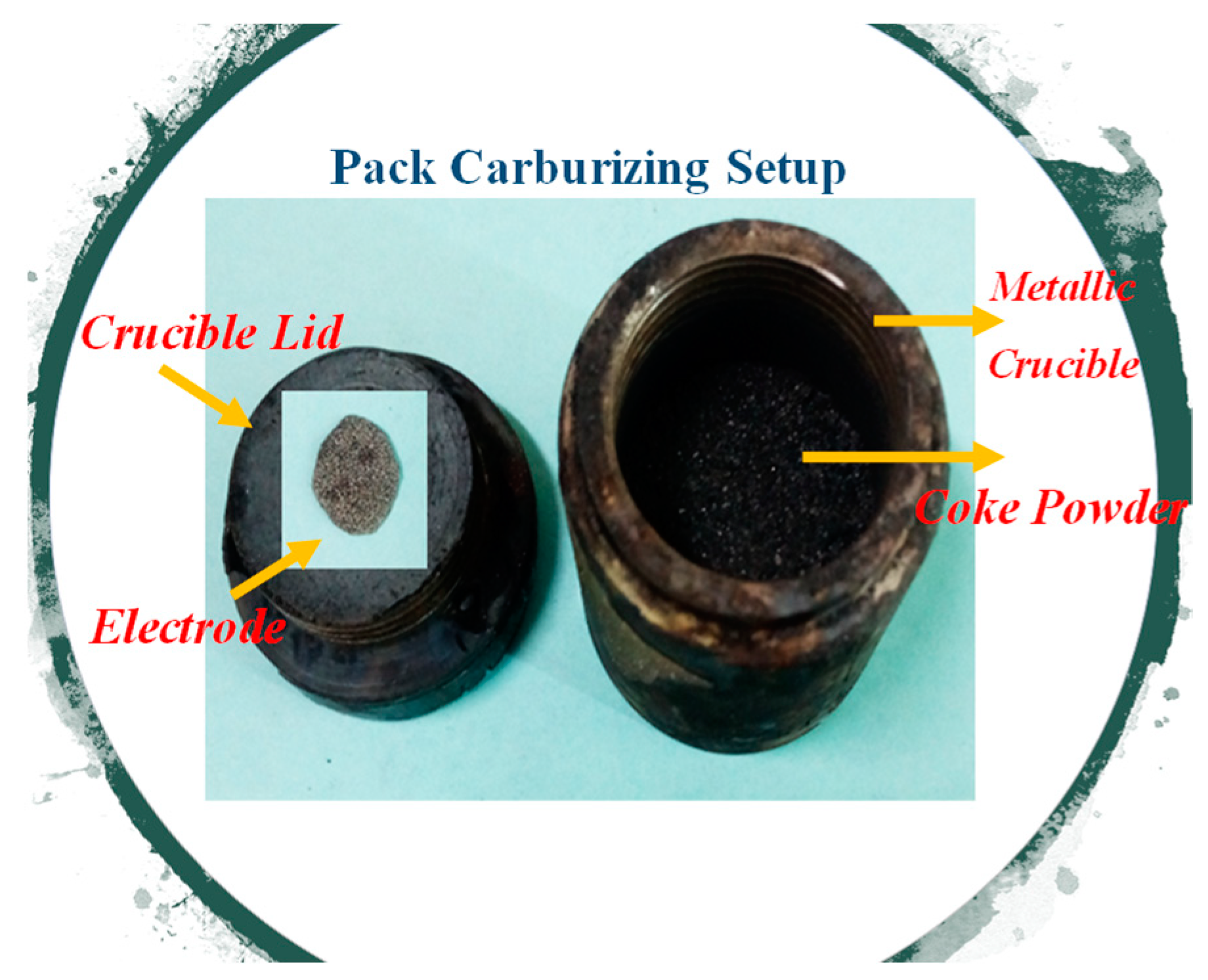
Carburization is a very well known method established decades ago by the steel industry and used in case-hardened steel using lower carbon quantities. In this process, steel is inserted for a certain amount of time into high-carbon environments at a higher temperature range, and quenched quickly to a low temperature. Because of this quick quenching, the carbon is not allowed to resurface and becomes absorbed or trapped by the crystal structure. However, it can be a vital concern to experimentally demonstrate the diffusion of carbon atoms to obtain graphene on a few layers of nickel foam (Ni foam) for the supercapacitor electrode. In this study, a facile and cost-effective method of graphene synthesis by slight modification in the carburization process and its applications for supercapacitor electrodes is reported. Here, the graphene layer was grown on Ni foam by the diffusion of carbon into the Ni foam by the pack-carburizing method, and then naturally cooled to precipitate carbon for the in situ growth of graphene by decarburization, which was the area yet to be investigated.
3. Results and Discussion
Special lattice structure, high electrical conductivity, low cost, light weight, high specific surface area, and excellent electronic, chemical, and thermally stable properties make graphene a promising material for supercapacitor-electrode applications. Graphene was used as an electrode, and values were tested by using a binder. The electrode material was often bound to the current collector. The binder was electrochemically inactive, which reduced the available electrode surface area and resulted in lower specific capacitance (Csp) [
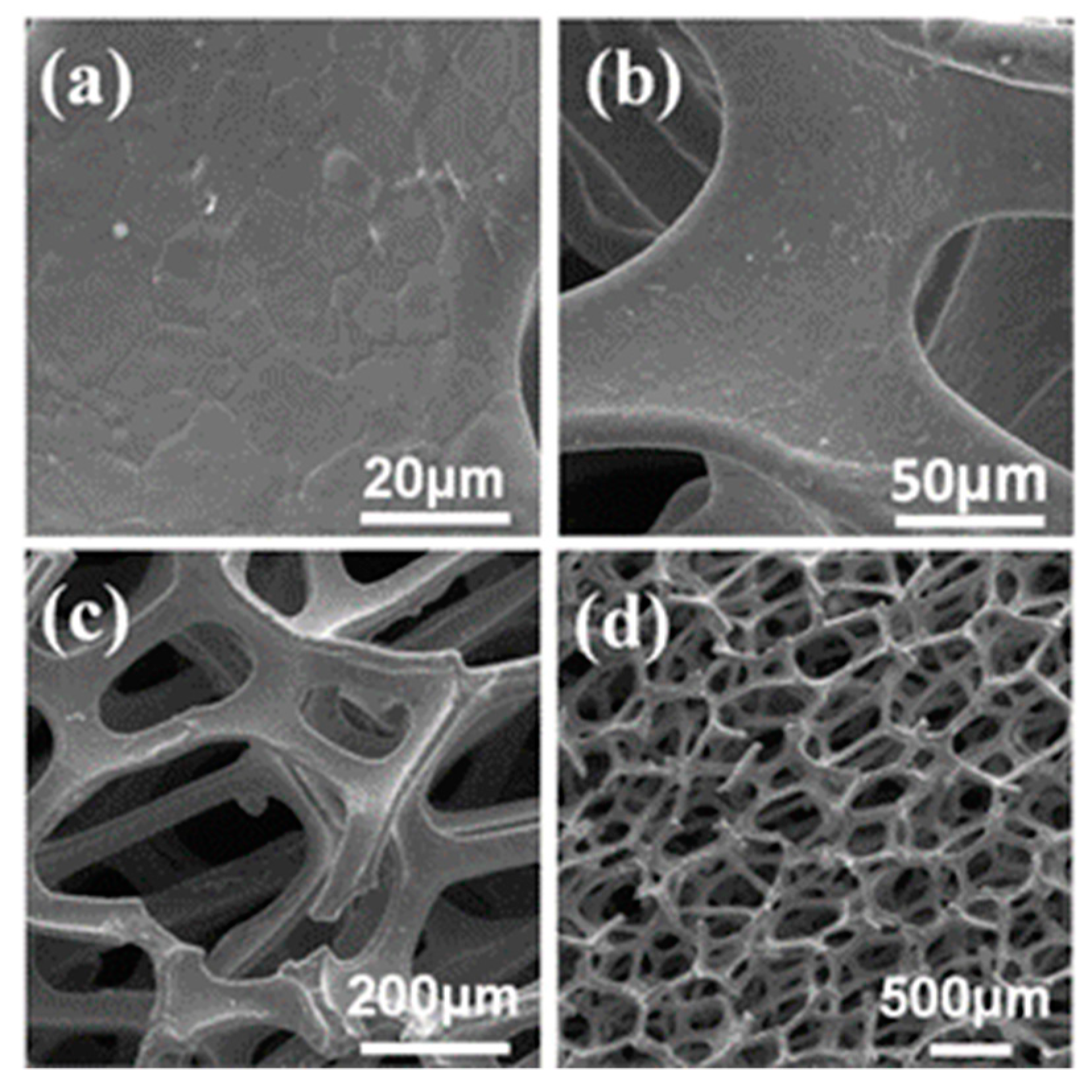
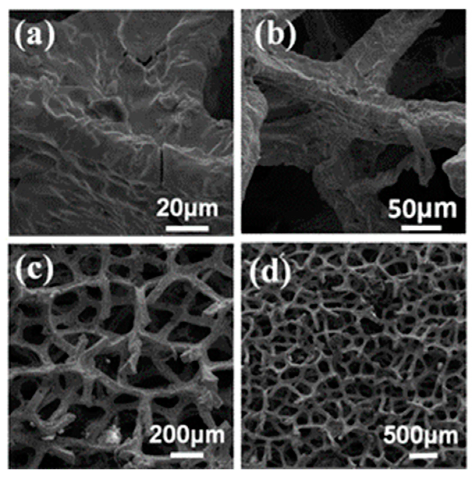
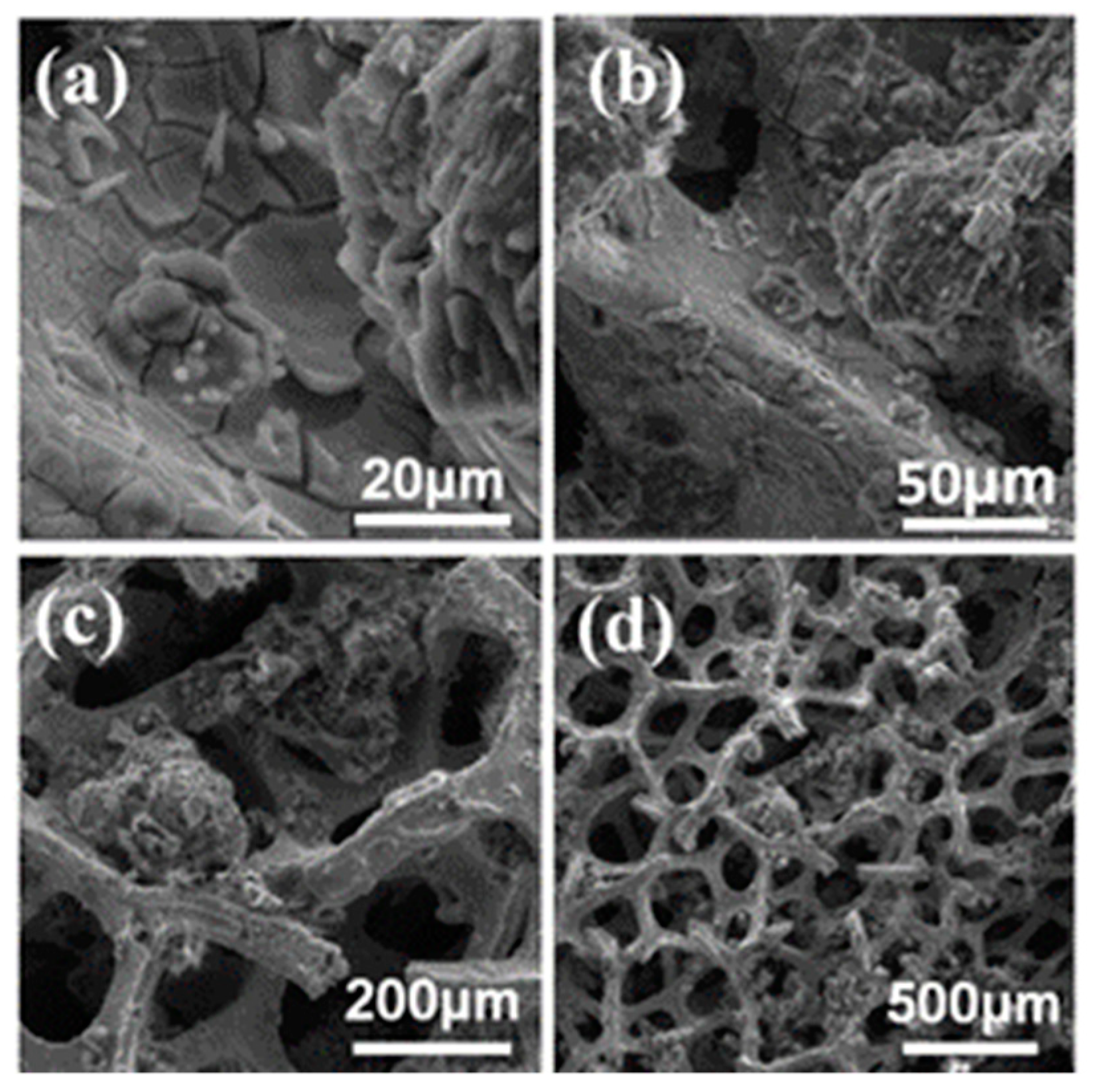
18]. In this work, an attempt was made to grow the graphene layer on Ni foam by the diffusion of carbon into Ni foam using the pack-carburizing method and natural cooling to precipitate carbon for the in situ growth of graphene by decarburization. Structural characterization was performed through SEM and Raman’s spectroscopy. Electrochemical characterizations such as cyclic voltammetry (CV), galvanic charge discharge (GCD), and electrochemical impedance spectroscopy (EIS) were performed using a potentiostat. The SEM images of bare Ni foam, GM1, and GM2 are depicted in
Figure 2,
Figure 3 and
Figure 4, respectively. SEM analysis of the bare Ni foam, as illustrated in
Figure 2 at different magnification levels, clearly shows a uniform porous and smooth structure. Average wire thickness of the foam was 47 µm, as shown in
Figure 2c. Many pores were present in the nickel framework with a cross-linked structure, and their sizes were in the range of 180–350 μm. The peculiar porous network framework could not only boost the intact area between current collectors and active materials, but also reduce the diffusion and migration tracks of electrolytic ions, resulting in better electrochemical performance. Given the different thermal-expansion coefficients between the nickel and growing film, ample ripples and wrinkles were created in the films. When incorporated with all other components to form composite materials, such ripples and wrinkles likely lead to better adhesion.
Further, SEM extrapolation showed that all nickel substrates were wrapped up in growth material after heat treatment and cooling, as depicted in
Figure 3d and
Figure 4d. Growth on GM2 due to the thicker growth structure had straight ridges and opaque surfaces (
Figure 4d). This means that GM2 had more graphene layers than GM1. In all scenarios, the three-dimensional Ni foam structure was retained due to the schematic effect driven by the structure, as shown in
Figure 2c,
Figure 3c and
Figure 4c.
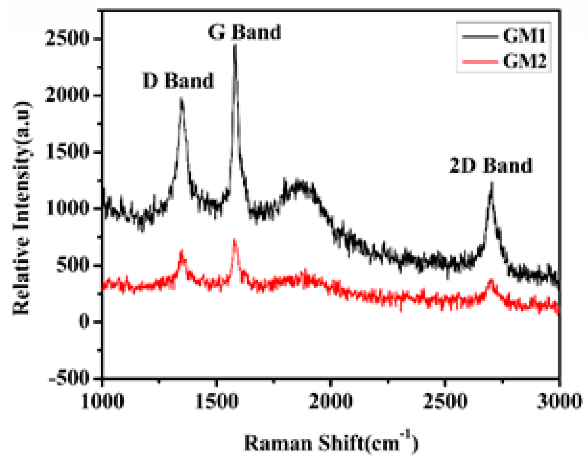
Raman spectroscopy was performed for GM1 and GM2 (see
Figure 5) using a laser of 50 mW power with excitation (wavelength, 532 nm), 40X objective lens, three scans, and integration times of 30 sec to obtain Raman spectra with Raman shift (cm
−1) on the X plane and relative intensity (a.u) on the Y plane, and study the crystalline quality and number of layers of the synthesized graphene [
28].
Carbon materials have been extensively characterized by Raman spectra with typical G and D bands prone to defects, disorder, and carbon-grain size. The typical Raman’s spectra of graphene and graphite consist of a D band, named the defective or disordered band, the G band, named an ordered band, and 2D second order D band [
29]. The main feature of the Raman’s carbon spectra is so-called G and D peaks that are for visible excitations at around 1560.0 and 1360.0 cm
−1, respectively [
30]. The peak positions of the D, G, and 2D bands for GM1 were 1347.09, 1582.69, and 2703.58 cm
−1; and for GM2, they were 1350, 1580.28, and 2700 cm
−1, respectively. The noticeable shouldering on the G band could have been due to the high D/G peak ratio indicating crystalline defects. In single-layer graphene, the D band resulting from disorder is small and rises in intensity with the number of layers [
5]. The intensity ratio of D band to G band is calculated and referred to as the R value for the study of graphitic materials [
6,
7]. The R value of both GM1 and GM2 was 0.80 and 0.87, respectively, indicating poor quality and a more defective structure. In addition, the 2D band was responsive to the number of layers. The number of layers of graphene film can also be identified by the shape and position of the 2D band, and the peak intensity ratio of 2D to G (I2D/IG) [
31]. In the case of GM1, the 2D band’s peak position was clearly upshifted and extended. The I2D/IG ratio for GM1 and GM2 was 0.5, which confirmed a smaller number for synthesized graphene. The G-band location gives insight into the number of present layers, and the width of the G band often follows a consistent pattern that can be utilized to obtain the thickness of the graphene. Wall et al. showed single-, double-, and triple-layer graphene spectra [
28]. The size of this band closely followed a linear trend as the sample transitioned from single- to multilayer graphene. The I2D/IG ratio of these bands for single-layer graphene of high quality (defect-free) can be shown to be equal to 2. Such a ratio, lacking a D band, and a sharp 2D symmetry are commonly utilized as evidence for a graphene-free graphene sample with high-quality defects.
To explore the electrochemical behavior of the as-prepared electrode, CV, GCD, and EIS characterization was carried out systematically for their electrochemical properties.
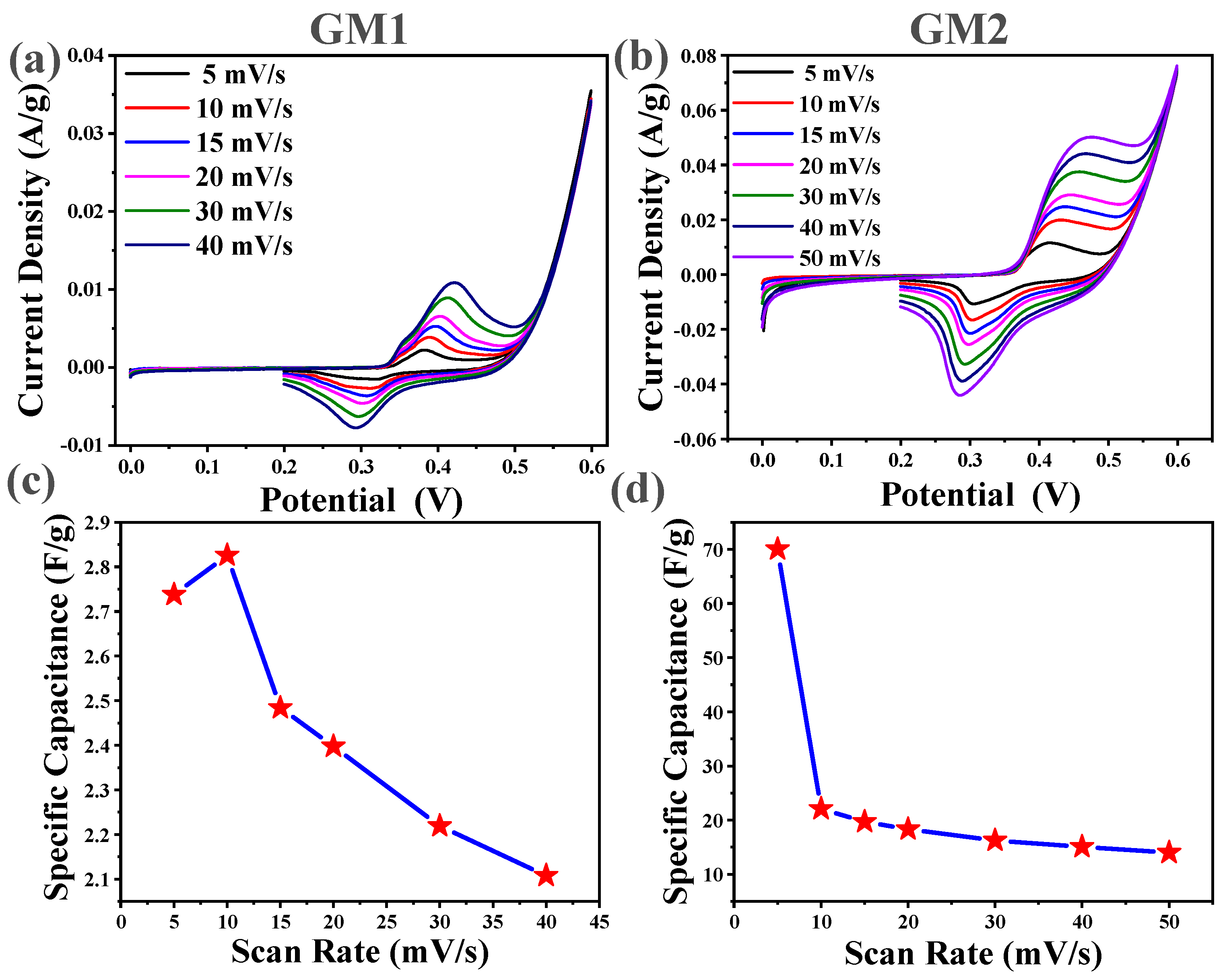
Figure 6 represents the CV curves of GM1 and GM2 in 6 M KOH electrolyte at different scan rates in the 0.0–0.6 volt (V) potential window, respectively. The Ag/AgCl electrode was used as a reference electrode, and platinum wire was used as the counterelectrode. The CV curves of GM1 and GM2 showed few notable redox peaks that indicated reversible Faradaic redox reactions associated with electrolyte ion intercalation/extraction. The cathodic peak was strategically placed at 0.3 V at a negative current value in the case of GM1, and 0.28 V in the case of GM2, corresponding to that of an electrolyte-intercalation reduction process. The identified positive-current-value anodic peak occurred at 0.42 V in GM1, and 0.45 V in GM2, leading an oxidation route associated with the oxidation cycle.
The Csp. of GM1 and GM2 from the CV curve is calculated using the following equation [
32].
where
A is the area underneath curve CV,
S is the rate of scanning (v/s),
m is the active mass of the used material, and ∆
v is the potential window used. Csp was computed using CV curves for GM1 (active mass, 0.0243 g) and GM2 (active mass, 0.0182 g); electrodes were 2.74 and 70.03 F g
−1 at 5 mVs
−1, respectively, and 2.11 and 15.07 F g
−1 at 40 mVs
−1. The capacitances of GM2 electrodes were observed to be larger than those of GM1 electrodes. GM2 showed better electrochemical properties as than those of GM1. As previously reported, graphene on nickel foam grown by CVD in a hydrogen and methane environment at different cooling rates showed a Csp. Near about 55.3 F g
−1 at 5 mv/s [
33]. Results are comparable with those of previous studies. When the scanning rate increased, the capacity of both GM1 and GM2 decreased, as shown in
Figure 6. As scan rate increased, it also raised the current but reduced the Csp. Assuming that decelerating the scan rate may enable electrolytes to more deeply penetrate the pores, and allow for further contact with the electrode material’s internal surface, thereby allowing for more charge to be deposited on the electrode surface, this results in greater measured capacity closer to the intrinsic power. At a high scanning rate, electrolytes and electrodes interact for quite a limited amount of time, resulting in lower charge accumulation on the surface of the electrode and thus low capacitance [
34]. GM2 possessed higher Csp. than that of GM1. This observation can be related to the easy transportation of electrons from graphene to the current collector in GM2 resulting from the greater interaction of graphene films with the substrates.
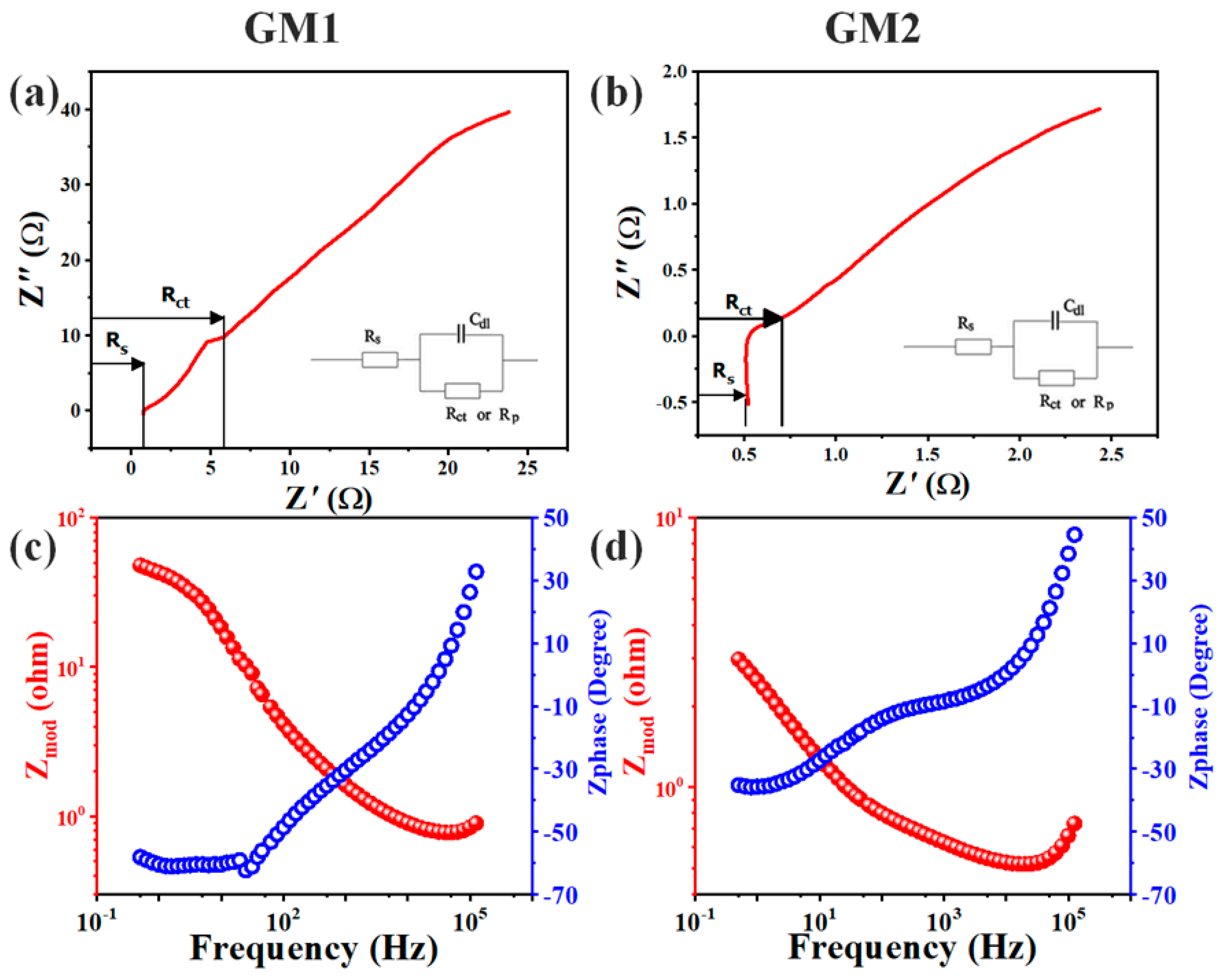
Electrochemical-impedance measurements were performed at frequencies ranging from 0.5 Hz to 100 KHz in order to further investigate the electrochemical activity of the GMs. The impedance spectrum could be evaluated using a Nyquist plot (
Figure 7a,b) and Bod plot (
Figure 7c,d). The GM’s impedance spectrum was evaluated using Nyquist plots, showing the imaginary component of impedance Zimg (ohm) against actual component Zreal (ohm), as shown in
Figure 7a,b for GM1 and GM2. Every data point with the lower-left portion of the plot referring to higher frequencies was at a different frequency. In the Nyquist plots, the x-intercept on the Zreal (ohm) axis indicated entire system resistance known as equivalent series resistance (ESR) comprising solution resistance (Rs), charge transfer resistance between electrolyte and electrode (Rct), and collector resistance known as Rz. Solution resistance (Rs) defines the rate at which the films can be charged or discharged. The Rs value for GM2 was small, in the range of 0.5 ohm, suggesting the excellent power capabilities of the sample as compared to those of GM1, but the difference was very small because both samples were tested in same solution. The mechanism of double-layer charging in a medium-frequency range gave rise to the semicircular curve. The increased resistance was attributed to the transfer of charge (Rct) and the resistance to mass transportation. At low frequencies, a sloppy line indicates the electrode materials’ ideal capacitive behavior. At low frequencies, impedance is the sum of electrolyte resistance and charge-transfer resistance; at higher frequencies, only solution resistance is present because at higher frequencies, impedance is present because the transfer of charges at the electrode–electrolyte interface is negligible. Therefore, only electrolyte resistance or solution resistance is present at lower frequencies. The impedance of the system can also be represented as a Bode plot between the frequency on the X axis and the modulus of impedance in ohm on the left y axis, and impedance phase in degree on the right y axis. The Bode plot plotted for GM1 and GM2 is shown in
Figure 7c,d. The modulus of impedance for GM1 at low frequencies, as depicted in
Figure 7c, was higher and gradually decreased as frequency increased from left to right. The maximal modulus of impedance at the low frequency of 0.5 Hz was recorded at 47.9 ohm, and the minimal modulus of impedance at a higher frequency of 100 KHz was observed at 0.84 ohm for GM1. Similarly, for GM2, as shown in
Figure 7d, the modulus of impedance was higher at low frequencies and decreased gradually from left to right as frequency increased. Such behavior was shown by the electrochemical system because at a higher frequency, no charge-transfer resistance was present. At the low frequency of 0.5 Hz, the maximal modulus of impedance for GM2 was noted at only 2.98 ohm; at the higher frequency of 100 kHz, it was noted at 0.67 ohm. These values were similar to the values in the Nyquist plot. The lower-impedance values for GM2 as compared to GM1 corresponded to its better electrochemical performance, as discussed in CV and GCD. The impedance phase had a direct relation with frequency and gradually increased as frequency increased from left to right. The impedance-phase value for GM1 at the low frequency of 0.5 Hz and high frequency of 100 KHz was observed at −58.1° and 26.29°, respectively. Similarly, for GM2, the impedance-phase value at the lower frequency of 0.5 Hz was −35.1°, while at a higher frequency, it was 38.5°.
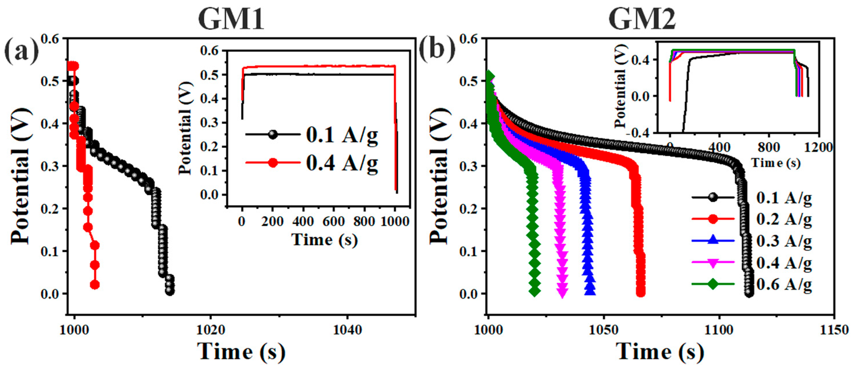
At current density of 0.1 to 0.6 Ag
−1, galvanic charge–discharge was performed while observing charge/discharge efficiency. The GCD curve of samples GM1 and GM2 is shown in
Figure 8. Csp. was calculated from the GCD curve using the following equation [
32].
where
I is the current of discharge,
t is the time of discharge,
m is the active mass of the electrode, and
v is the potential window applied. The Csp. calculated for GM1 was 2.3 and 2 F/g at current density 0.1 and 0.4 A/g, respectively, revealing poor performance. Csp. for GM2 was 18.83, 22, 22, 21.33, and 20 F/g at current density of 0.1, 0.2, 0.3, 0.4, and 0.6 A/g, respectively, showing better performance than that of GM1.
The energy density and power density of the GM1 and GM2 samples were determined using the following equations.
where
C is
Csp., and ∆
v is the potential window.
The energy and power densities for GM1 at current density of 0.4 A/g were observed to be 0.1 Wh/kg and 120 W/g, respectively. Likewise, for GM2, energy and power density at current density of 0.6 A/g was observed at 1.008 Wh/kg and 180 W/kg, indicating better results.

 ,
, 


