Abstract
KTa0.65Nb0.35O3 and Fe-doped KTa0.65Nb0.35O3 crystals were grown by the top-seeded solution growth method (TSSG). Fe ion doping significantly improves the electro-optic properties of cubic KTN crystals. We describe their electro-optic modulation theory and experimental research. The electro-optic modulation waveform deduced by theoretical calculation is basically consistent with the waveform measured in the experiment. We observed the attenuation of light modulation under multiple voltage cycles. The modulation curve of the crystal is inconsistent when the crystal voltage is boosting and bucking. Under the same voltage condition, the higher the incident light power, the faster the modulation depth attenuation. In this experiment, the size of the KTN crystal chip is 6 mm × 5 mm × 2 mm. We obtain the effective electro-optic coefficient as s11 − s12 = 1.34 × 10⁻¹⁵ m2/V2; the half-wave voltage near the Curie temperature is 39 V.
1. Introduction
An electro-optic modulator (EOM) is a signal-controlled device that can be used to control the intensity, phase and polarization status of a laser beam. It is widely used for high-speed optical communications, Q-switching of solid-state lasers, and active mode locking [,,]. For traditional linear EOM based on LiNbO3 [] and lead lanthanum zirconate tantalate (PLZT) [], the electro-optic effect is a linear electro-optic effect (Pockels Effect), and thus the electro-optic coefficient is relatively low. However, the potassium tantalum niobate crystal (KTN) is a special case and it exhibits the largest ever known quardratic electro-optic coefficient (about 70 times larger than that of lithium niobate). The large electro-optic coefficient confers the KNT-based modulators’ obvious advantages over the other electro-optic modulators, such as low drive voltage, small device size, high intrinsic modulation bandwidth and multiple composite functions [].
As KTN is a solid-solution mixed crystal of KTaO3 (KT) and KNbO3 (KN), it is difficult to obtain high-quality single crystals. In 2006, researchers used the top-seed solution growth method to obtain optically homogeneous KTN crystals with volumes of more than 30 cm3; this creates conditions for the actual electro-optical application of KTN crystals []. Ion doping is a common method to improve and adjust the physical properties of crystals. For example, Li+ and Na+ doping can effectively change the thermal expansion properties of KTN crystals []. In addition, researchers have found that copper and iron doping in KTN crystals of the tetragonal system can greatly improve the photorefractive properties of crystals [,]. The photorefractive effect and the electro-optic effect are similar in physical mechanism, which inspired us to develop an ion doping method in cubic crystal to improve its electro-optical properties.
In this paper, we use a top-seeded solution growth method to grow KTN and Fe-doped KTN crystals, and compare the influence of Fe doping on the dielectric constant. We describe its electro-optic modulation expression and execute experimental research based on the Fe: KTN quadratic electro-optic effect. The influence of the laser power and voltage on electro-optical intensity modulation was studied. The dielectric relaxation effect caused by polarized nano-regions (PNRs) was also discussed.
2. Theoretical Analysis on the EO Modulation of KTN
The experimental setup for electro-optic intensity modulation is shown in Figure 1. For KTN crystal in the cubic phase, when the electric field (E) direction is along the y direction, and , the refractive index ellipsoid changes from a sphere to an ellipsoid, and the crystal has optical anisotropy. The change of the refractive index model is expressed as
where n0 is the refractive index of the crystal without the application of electric field; nX, nY, nZ, respectively, are the refractive indexes of the crystal in the corresponding direction after the electric field is applied. E is the applied electric field intensity, s11 and s12 are the quadratic electro-optic coefficients. When the incident light propagates along the z-axis direction, the polarization direction of the polarizer is 45°; the polarization direction of the analyzer is perpendicular to it, and the change in light intensity can be expressed as
where L is the crystal length in the light passing direction, d is the electrode distance, λ is the incident light wavelength.
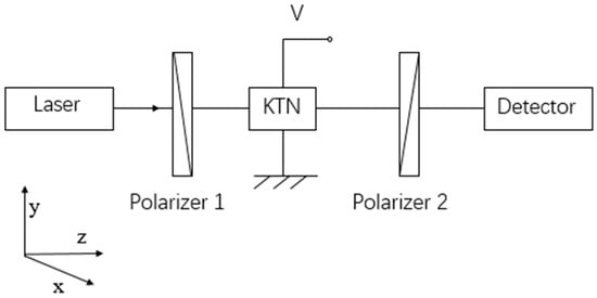
Figure 1.
A diagram of experimental light path.
The top-seed solution growth method (TSSG) was used to grow KTa0.65Nb0.35O3 and Fe: KTa0.65Nb0.35O3 crystals in a platinum crucible. Reagents of K2CO3, Ta2O5, Nb2O5, and Fe2O3 (purity 99.99%) were used as raw materials for the crystal growth. The addition of Fe2O3 was 0.1 wt %. This is a better Fe doping concentration that we found through experiments []. The crystals were grown in a crystal-pulling apparatus. A KTN single-crystal bar with dimensions of 3 mm × 3 mm × 25 mm was used as the seed. The crystal pulling speed is 0.3 mm/h and was rotated at a rate of 5 rpm during growth. After five days of growth, it is slowly cooled to room temperature at a rate of 30 °C/h. We prepared KTN chips with a size of 6 mm × 5 mm × 2 mm and polished their surfaces. The magnetron-sputtering coating equipment was used to plate gold electrodes on both sides of the crystal.
We put the crystal chip into a LCR digital electric bridge (HIOKI 3532-50) to measure the capacitance, and use the equation to calculate the relative dielectric constant of the crystal.
where is the vacuum dielectric constant, d is the thickness of the crystal, C is the capacitance measured by the dielectric temperature measuring instrument, and S is the area of the electrode.
Figure 2 shows the relative permittivity εr of pure KTN and Fe: KTN crystals with the same ratio as Ta and Nb, as a function of temperature. We also measured the temperature dependence on the dielectric constant of Fe: KTN crystals at different frequencies. Fe ion doping can significantly improve the relative permittivity εr of cubic KTN crystals. Starting from −50 °C, the relative permittivity εr of Fe: KTN crystals gradually increases with the increase in temperature, reaching a maximum value of about 16,700 at the Curie temperature (TC = 4 °C). The value of Nb/(Nb+Ta) can be obtained by the following empirical equation.
where X is the value of Nb/(Nb + Ta) and the unit of TC is absolute temperature []. We calculate the value of X to be 0.35. As the temperature continues to increase, the relative permittivity εr begins to decrease. The relationship between relative dielectric constant εr and Kerr constant is [].
where gij is the g coefficient (quantifying nonlinearity of the medium, the change in the refractive index with the optical intensity). The g factor is a function of wavelength, and is related to the crystal structure and independent of dielectric constant []. According to reports, the g coefficients of KTN are g11 = 0.136 m4/C2 and g12 = −0.038 m4/C2 []. By putting the maximum value of εr in Figure 2 into Equation (6), we get the effective electro-optic coefficient as s11 − s12 = 1.34 × 10⁻¹⁵ m2/V2. It is dozens of times the electro-optic coefficient of traditional materials such as LiNbO3 [].
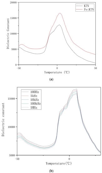
Figure 2.
(a) Dielectric constant εr of potassium tantalum niobate (KTN) and Fe: KTN crystals changes with temperature. (b) Temperature dependence of the dielectric constant of Fe: KTN crystal at different frequencies.
We put the effective electro-optic coefficient into Equation (3) to simplify the relationship between light intensity and voltage. Then, we used V as the abscissa and normalized I as the ordinate to make Figure 3. It can be seen that the half-wave voltage gets lower and lower, which should be caused by V2 in Equation (3); this shows that the quadratic electro-optic effect does play a major role at this time.
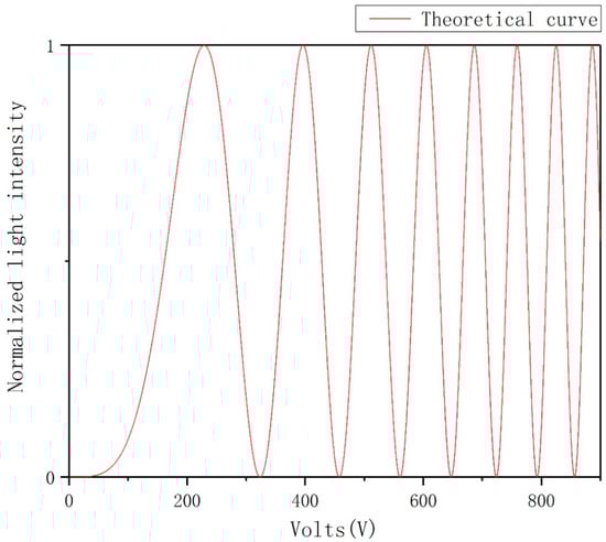
Figure 3.
Theoretical curve calculated and simulated by the effective electro-optic coefficient.
3. Experiment and Discussion
As shown in Figure 4, the light source was a linearly polarized He-Ne laser (λ = 638 nm). The laser light passes through the polarizer, Fe: KTN crystal and the analyzer, and is finally received by the detector. The polarization axes angle between the polarizer and the analyzer is 90 degrees. The voltage signal sent by the function generator is amplified by the high-voltage amplifier and applied to the two electrode surfaces of the crystal. Using the thermoelectric couple (TEC) semiconductor refrigerator, the temperature of the crystal is controlled to be stable at 17 °C.
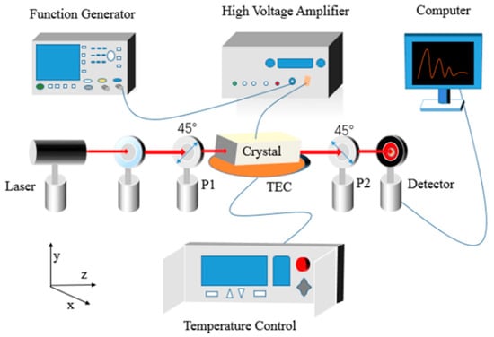
Figure 4.
Schematic representation of the experimental optical path.
Figure 5 shows changes in the intensity of the output light under applied voltage. The first maximal output light modulation is reached at 221 V. With a local minimum around 332 V, the phase shift is 2π. The second local maximum is around 415 V, and the phase shift reaches 3π. The value of the half-wave voltage () is 221 V at 17 °C. The amplitude of the light intensity maintains good stability with slow attenuation. Compared to the theoretical curve in Figure 3, the experimental results are basically consistent with the theory, which verifies the accuracy of this experiment.
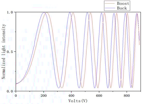
Figure 5.
Curve of light intensity modulation when a sinusoidal voltage of 0 to 900 V is applied at 17 °C.
Due to the influence of certain stresses and defects such as internal traps in the crystal, the initial light intensity in the figure is not zero. It can be clearly observed that the two process curves of boost and buck are inconsistent. This indicates that there is more than one phase in the crystal. The applied voltage leads to the existence of polarized dipoles of the ferroelectric phase in the paraelectric phase. It also shows that PNRs exist during the crystal relaxation phase transition [].
The Curie temperature of the crystal is 4 °C, and the temperature of the buck-boost experiment on the crystal is 17 °C, far from the Curie point. As we all know, when the temperature is in the range above the Curie point, the electro-optic coefficient is the largest at this time, and the electro-optic effect will be significantly enhanced. Therefore, we can predict that, when closer to the Curie point, the half-wave voltage of the crystal electro-optic modulation will drop significantly. We used TEC equipment to measure the half-wave voltage changes in crystals at different temperatures. As shown in Figure 6, the half-wave voltage of the crystal near the Curie point can be reduced to 39 V.
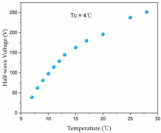
Figure 6.
Change of half-wave voltage with temperature.
Figure 7 records 8 complete voltage cycles. The voltage increases from 0 to 1200 V and then decreases to 0 V in each voltage cycle. When the electro-optic modulation of the crystal is started, there is no obvious attenuation of the modulation depth in the first voltage cycle, and the modulation effect is good. After a few voltage cycles, the modulation depth is significantly attenuated when the voltage gradually increases from 0 to 1200 V in a single voltage cycle. The modulation depth gradually recovers when the voltage gradually decreases from 1200 to 0 V. However, the modulation depth at the beginning of the experiment has not been restored. The polarization characteristics in KTN crystals mainly come from the displacement of niobium ions []. The displacement of niobium ions causes the microscopic local symmetry of KTN crystals to be broken when voltage is applied to the crystal, resulting in dipoles on the lattice scale. As the applied voltage increases, the random movement of polarized dipoles in the crystal decreases, and they may group together to form larger-sized PNRs [,]. Random scattering occurs when incident light enters this area, resulting in crystal depolarization and attenuation of the modulation depth.
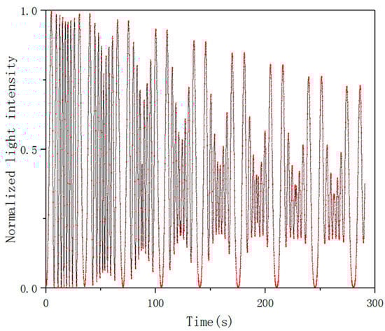
Figure 7.
Changes in the modulation curve after multiple voltage cycles.
It should be noted that the power of the incident light used in the above two sets of experiments is different. When boosting and bucking the crystal, the incident light power set in the experiment is 10 μW. But when testing in several cycles, the incident light power at that time is 5 mW. In other words, there is a possibility that the power change of the incident light in the experiment caused the different experimental results. Therefore, we decided to test under different incident light conditions.
From Figure 8 we can see that when the incident light is 0.4 mW, the modulation curve has no obvious attenuation. With the continuous increase in the incident light power, the attenuation of the optical modulation depth is accelerated, and there is a significant phase delay. We think that this phenomenon is caused by the photorefractive effect. At this time, the photorefractive effect occurred in the KTN crystal. When light is applied, impurities, vacancies, and defects in the crystal are excited by absorbing the energy of the light and generate electrons or holes. These optically excited charge carriers diffuse and drift, and are captured by the trap during migration. Then, they continue to absorb energy and to be excited until the carriers move out of the illuminated area and are captured in the dark area. These processes result in the formation of a spatial distribution of positive and negative charges. As a result, a space charge field is formed within the crystal. This will cause distortion of the lattice, which results in a series of changes, such as the displacement of niobium ions, the asymmetry of KTN crystal at the micro level, and generation of polarized dipoles on the lattice scale. All of these lead to the changes in the refractive index inside the crystal []. The incident light is scattered, resulting in a phase delay of the modulated light intensity and attenuation of the modulation depth. When the incident light intensity is increased and the time is longer, the crystal absorbs the photon energy faster and it is easier to generate optically excited charge carriers and to form a space charge field. This results in a worse modulation effect.
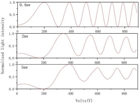
Figure 8.
Modulation curve of light intensity under different powers of incident light.
These are problems that need to be solved and avoided in practical applications. The studies of these modulation phenomena help us to further understand the law of crystal electro-optic modulation, and provide guidance for reducing crystal internal defects and growing crystals with better optical quality. Our laboratory has recently done a lot of work in improving the optical quality of crystals. For example, using a large crucible to grow small crystals and intelligent software to control the growth, crystals with more uniform composition, fewer internal defects, effectively reduced PNRs and better optical quality are grown. Compared with traditional linear electro-optic crystals, KTN crystals have the characteristics of low driving voltage, small size, and good modulation effect. They are expected to be widely used in laser display, radar, communication technology and other fields.
4. Conclusions
We have grown the KTa0.65Nb0.35O3 and Fe-doped KTa0.65Nb0.35O3 crystal by the top seed solution method (TSSG), and described its electro-optic modulation theory and experimental research. The quadratic electro-optic coefficient of the crystal was measured and calculated, and the optical modulation waveform was derived through theoretical calculation. After comparison, it was found to be basically consistent with the waveform measured in the experiment, which verified the accuracy of the theoretical calculation and experiment. The electro-optic modulation curves are inconsistent when voltage is boosting and bucking. The greater the applied voltage, the faster the amplitude of the optical emphasis system decay; as the initial optical power continues to increase, the rate of modulation depth attenuation also accelerates. These phenomena indicate the existence of PNRs in the crystal. In this experiment, the size of the chip is 6 mm × 5 mm × 2 mm, the effective electro-optic coefficient of KTN crystal is s11 − s12 = 1.34 × 10⁻¹⁵ m2/V2. The half-wave voltage near the Curie temperature can drop to 39 V. The large effective electro-optic coefficient makes possible small devices and lowers the driving voltage of the crystal used for EOM and other situations, which is in the further exploration.
Author Contributions
Writing—original draft preparation, C.-K.Y.; writing—editing, X.-P.W.; conceptualization, F.Z.; data curation, H.-D.Z.; methodology, B.L.; Visualization, J.L.; investigation, Y.-Y.Z.; Validation, Y.-G.Y.; project administration, X.-S.L.; software, L.W. All authors have read and agreed to the published version of the manuscript.
Funding
This research was funded by National Natural Science Foundation of China (51772172, 51972179 and 51902168); Major Scientific and Technological Innovation Project in Shandong (2018CXGC0412); Natural Science Foundation of Shandong Province (ZR2018BEM023); Science and Technology Program for Young Innovation Team in Colleges and Universities of Shandong Province, China (2019KJA003).
Conflicts of Interest
The authors declare no conflict of interest.
References
- Dolne, J.J.; Xu, J.; Zhi, Y.N.; Wang, X.; Sun, J.; Zhou, Y.; Dai, E.; Liu, L.; Karr, T.J.; Gamiz, V.L.; et al. A large-angle high speed scanner based on electro-optic crystal for Fresnel telescope synthetic aperture imaging ladar. In Proceedings of the Unconventional Imaging and Wavefront Sensing, San Diego, CA, USA, 13–14 August 2012. [Google Scholar]
- Li, Y.; Li, J.; Zhou, Z.; Guo, R.; Bhalla, A. Low-frequency–dependent electro-optic properties of potassium lithium tantalate niobate single crystals. EPL Europhys. Lett. 2013, 102, 37004. [Google Scholar] [CrossRef]
- Miyazu, J.; Imai, T.; Toyoda, S.; Sasaura, M.; Yagi, S.; Kato, K.; Sasaki, Y.; Fujiura, K. New Beam Scanning Model for High-Speed Operation Using KTa1−xNbxO3 Crystals. Appl. Phys. Express 2011, 4, 111501. [Google Scholar] [CrossRef]
- Bosco, A.; Boogert, S.T.; Boorman, G.E.; Blair, G.A. A large aperture electro-optic deflector. Appl. Phys. Lett. 2009, 94, 211104. [Google Scholar] [CrossRef]
- Cutchen, J.T. PLZT thermal/flash protective goggles: Device concepts and constraints. Ferroelectr 1980, 27, 173–178. [Google Scholar] [CrossRef]
- Nakamura, K. Optical Beam Scanner Using Kerr Effect and Space-charge-controlled Electrical Conduction in KTa1−xNbxO3 Crystal. NTT Nec Tech. Rev. 2007, 5, 1–8. [Google Scholar]
- Tadayuki Imai, M.S.; Fujiura, A.K. Crystal growth and electro-optic properties of KTa1−xNbxO3. Growth Technol. Device 2007, 5, 1–8. [Google Scholar]
- Li, Y.; Li, J.; Zhou, Z.; Guo, R.; Bhalla, A. Thermal expansion behavior and polarization properties of lead-free ferroelectric potassium lithium tantalate niobate single crystals. Ceram. Int. 2014, 40, 1225–1228. [Google Scholar] [CrossRef]
- Mu, X.; Shao, Z.; Yue, X.; Chen, J.; Guan, Q.; Wang, J. High reflectivity self-pumped phase conjugation in an unusually cut Fe-doped KTa1−xNbxO3 crystal. Appl. Phys. Lett. 1995, 66, 1047–1049. [Google Scholar] [CrossRef]
- Guan, Q.; Wang, J.; Lian, Y.; Yang, C.; Ye, P. Influences of iron doping on the photorefractive properties of KTa1−xNbxO3 crystals. Appl. Phys. Lett. 1993, 63, 2186–2188. [Google Scholar] [CrossRef]
- Yu, H.-J.; Hu, Y.-Y.; Zhang, F.; Yang, C.-K.; Zhang, H.-D.; Li, J.; Zhang, Y.-Y.; Wang, X.; Liu, B.; Wei, L. Solvothermal synthesis and effects of Fe-doping on KTa0.63Nb0.37O3 nanocrystallines. Inorg. Nano Met. Chem. 2020, 1–4. [Google Scholar] [CrossRef]
- Rytz, D.; Chatelain, A.; Höchli, U.T. Elastic properties in quantum ferroelectric KTa1−xNbxO3. Phys. Rev. B 1983, 27, 6830–6840. [Google Scholar] [CrossRef]
- Geusic, J.E.; Kurtz, S.K.; Van Uitert, L.G.; Wemple, S.H. Electro-Optic Properties of some ABO3 Perovskites in the Paraelectric Phase. Appl. Phys. Lett. 1964, 4, 141. [Google Scholar] [CrossRef]
- Liu, D.D.; Ho, J.G.; Pastor, R.C.; Stafsudd, O.M. Sol-gel derived stoichiometric KTN. Mater. Res. Bull. 1992, 27, 723–729. [Google Scholar] [CrossRef]
- Chen, H. Optical Beam Scanning Using Potassium Tantalite Niobate. Master’s Thesis, University of Dayton, Dayton, OH, USA, 2015. [Google Scholar]
- Wang, C.; Zhang, M.; Stern, B.; Lipson, M.; Lončar, M. Nanophotonic lithium niobate electro-optic modulators. Opt. Express 2018, 26, 1547–1555. [Google Scholar] [CrossRef] [PubMed]
- Lu, Q.; Li, B.; Dai, H.; Ge, B.; Han, J. In situ observation and monitoring of the dynamic behavior of field-induced photorefractive grating formation process with digital holographic microscopy. Opt. Mater. Express 2016, 6, 2991. [Google Scholar] [CrossRef]
- DelRe, E.; Spinozzi, E.; Agranat, A.J.; Conti, C. Scale-free optics and diffractionless waves in nanodisordered ferroelectrics. Nat. Photon 2010, 5, 39–42. [Google Scholar] [CrossRef]
- Parravicini, J.; Agranat, A.J.; Conti, C.; DelRe, E. Equalizing disordered ferroelectrics for diffraction cancellation. Appl. Phys. Lett. 2012, 101, 111104. [Google Scholar] [CrossRef]
- Zhang, X.; He, S.; Zhao, Z.; Wu, P.; Wang, X.; Liu, H. Abnormal optical anisotropy in correlated disorder KTa1–xNbxO3: Cu with refractive index gradient. Sci. Rep. 2018, 8, 2892. [Google Scholar] [CrossRef] [PubMed]
© 2020 by the authors. Licensee MDPI, Basel, Switzerland. This article is an open access article distributed under the terms and conditions of the Creative Commons Attribution (CC BY) license (http://creativecommons.org/licenses/by/4.0/).