The Effect of Strain Rate on the Deformation Processes of NC Gold with Small Grain Size


1
Key Laboratory of Automobile Materials, Ministry of Education, and College of Materials Science and Engineering, Jilin University, Changchun 130012, China
2
Department of Material Science and Engineering, Rensselaer Polytechnic Institute, Troy, NY 12180, USA
3
Department of Physics and Astronomy, University of Missouri, Columbia, MO 65211-7010, USA
4
State Key Laboratory of Automotive Simulation and Control, Jilin University, Changchun 130012, China
*
Author to whom correspondence should be addressed.
Crystals 2020, 10(10), 858; https://doi.org/10.3390/cryst10100858
Submission received: 13 August 2020
/
Revised: 13 September 2020
/
Accepted: 17 September 2020
/
Published: 24 September 2020
(This article belongs to the Special Issue Crystal Plasticity at Micro- and Nano-scale Dimensions)
Abstract
:The strength of nanocrystalline (NC) metal has been found to be sensitive to strain rate. Here, by molecular dynamics simulation, we explore the strain rate effects on apparent Young’s modulus, flow stress and grain growth of NC gold with small size. The simulation results indicate that the apparent Young’s modulus of NC gold decreases with the decrease of strain rate, especially for strain rates above 1 ns−1. The rearrangement of atoms near grain boundaries is a response to the decrease of apparent Young’s modulus. Indeed, the flow stress is also sensitive to the strain rate and decreases following the strain rate’s decrease. This can be found from the change of strain rate sensitivity and activation volume with the strain rate. Temperature has little effect on the activation volume of NC gold with small grain size, but has an obvious effect on that of relatively large grain size (such as 18 nm) under low strain rate (0.01 ns−1). Finally, grain growth in the deformation process is found to be sensitive to strain rate and the critical size for grain growth increases following the decrease of strain rate.
1. Introduction
Nanocrystalline (NC) materials, especially NC metals and alloys, have attracted much attention due to their novel properties, such as improved wear resistance, high yield and high fracture strength [1,2,3]. It is well known that with the Hall–Petch rule the yield stress is increased following the grain size decrease from millimeter to submicron in coarse grained metals [4,5]. Interestingly, the range of application of the Hall–Petch rule about the yield stress and grain size can be expanded to nanoscale in NC metals such that the hardness and yield stress can increase 5–10 times, compared with their partners of coarse grain [6]. However, the micromechanism of the deformation processes in both regimes is considered to be different. In coarse grained metals, dislocations are generated from intragranular sources and they are stored and rearranged by the interaction between dislocation–dislocation. In NC metals, grain boundary mediated deformation is considered to control the strengthening [6,7,8,9,10,11].
The plastic deformation of NC metals may be related to many factors. Using grain size as the sole parameter to characterize its mechanical properties may be overly simplified, and thus sometimes give rise to uncertainties [12]. It has been revealed that the Hall–Petch rule breaks down when grain size decreases down to some critical size. To understand these novel results in experiments, even controversial findings [13,14], computer simulations at atomic level, especially molecular dynamics (MD), are expected to offer key insights. Indeed, MD is very helpful in understanding the deformation processes including plastic and elastic deformation, since it can provide real-time behavior and uncover the transient responses which are difficult to detect in experiments [15]. A lot of work has been taken to explore the critical size quantitatively and it is considered that the strength decreases generally as grain size decreases down to 20–10 nm. For example, the MD simulation showed that the critical size of NC Cu was about 10–15 nm [9].
It is well known that the mechanical response is always rate-sensitive [16,17,18]. For example, in the stainless steel, it was found that high strain rates (such as 104–105 s−1) could produce twin bundles with high density and nanoscale thickness [19]. Under high strain rates, such as pulsed shocking wave loading, it was found the shear and tensile strengths in metals could have very high values [18]. It is also noticed that the process of plastic deformation in NC metals is very sensitive to the loading rate [20,21]. In NC metals, the strain rate sensitivity (m) is an order higher than that of coarse grain [16,22,23]. It is considered that the large value of m is related to the interaction between grain boundaries (GBs) and dislocations in the plastic process. Another parameter, activation volume (V*) which is related to the m, is considered to affect the rate-controlling mechanism. The V* of NC metal is about two orders smaller than that of coarse grain [24,25]. Recently, many studies have found the m and V* are very helpful to quantify the deformation mechanism in NC metals further [10,11,17,26,27]. Experimental measuring [27] indicated the m of NC gold with a grain size of 30 nm was 0.01 under the strain rate above 10−4 s−1. Asaro et al. [17] showed theoretically that the value of m increased with the decrease of average grain size in NC metals, while the V* was increased with the increase of average grain size. Wang et al. found that the V* decreased with the increase of temperature in the NC Ni experiment with a grain size of 15 nm [10].
MD with its inherent constraints makes the time scale of simulation limited. The dynamics of the system is probed over just a few nanoseconds. Even with the quick development of computational techniques, the time period for the dynamics of a system with intermediate size (about 106 atoms) can be probed to be about 103 ns and thus the deformation of the system is simulated under very high strain rates, such as the typically used 1 ns−1 for deformation processes, corresponding to the strain of 0.1 in 0.1 ns. Through this limit of simulation time, we can modulate the strain rate to explore the deformation processes to provide some insights into the atomic mechanism. Some simulation works about strain rate on NC metals with small grain size have been performed [11,15,28,29,30]. For example, in simulations of NC copper with grain sizes of 2.1–11.5 nm, it was found that grain coarsening was closely related to strain rate [31]. The grain size of grain coarsening increased with the decrease of strain rate. The simulation on 2D NC copper with a grain size of 9 nm [26] showed Young’s modulus was kept almost constant at strain rates below 5 × 10⁵ s−1. When the strain rate was more than 5 × 10⁵ s−1, Young’s modulus increased with the increase of strain rate. However, there is still a lot of work needing to be undertaken. For instance, the mechanism of the change of elastic modulus with the strain rate isn’t fully understood. The temperature effect combined with the strain rate on the deformation processes needs to be explored further. The effect of strain rate on grain growth also needs to be studied in depth.
In this work, we use MD simulations to study the effect of strain rate on the mechanical behaviors and deformation mechanisms in NC gold with small grain size. Two models of NC gold are constructed. One is with an average grain size of 6 nm, and the other is with 18 nm. For the deformation under applied tensile strain, the strain rate is modulated from 0.01 per ns to 10 per ns. Two temperatures including 300 K and 800 K are adopted to combine the change of strain rate to explore the deformation mechanism. The simulation results clearly show strain rate effects on Young’s modulus, flow stress and grain growth of NC gold in tensile deformation and also reveal the atomic mechanism to some extent by combing the results from known experiments.
2. Computational Approach and Models
All the simulations were performed with standard molecular dynamics simulation (MD) methods which were implemented in large-scale atomic/molecular massively parallel simulator (LAMMPS) [32]. The atomic interaction (Vp) between gold atoms was constructed under the frame of embedded-atom method (EAM) potential and composed by a pairwise potential and a many-body embedding energy, as indicated by the formula,
where Ui,j (ri,j) was the pairwise potential for the atom at ri and that at rj, Ei was the embedding energy of atom at ri from the contributions of nearby atoms whose density was described by the item of . Here we used the parameters from Foiles et al. [33] to parameterize the EAM of gold. This potential can predict the mechanical properties of gold well. The simulated lattice constant of gold is 0.4078 nm and the stable lattice is fcc. The calculated Young’s modulus of polycrystalline gold with this potential is about 78 GPa and is consistent to the value from experiments.
The NC gold models were constructed with the Voronoi method which was popularly used for the building of atomic models for polycrystalline systems. Here the Voronoi method used was implemented in the program Atomsk [34]. We constructed the models of NC gold with average grain sizes of 6 nm and 18 nm, respectively. The periodic boundary conditions were applied for the three directions. To account for statistical effects, there are more than 15 Voronoi grains in each model. Grain orientations are random and the expected mean values (6 nm and 18 nm in two models) around distribution of grain size are used, as shown in Figure 1a,b.
It is known that the Voronoi approach is just the method of geometric construction with atoms in discrete lattice site. In atomic model of NC, it is popular that the atoms of GBs are unstable. In order to obtain the reasonable atomic configurations at GBs, we needed to relax the unfavorable atomic configurations at GBs. Thus, before the simulations of mechanical properties were performed, the atomic models of NC were annealed at room temperature for 100 ps. All the annealing processes were carried out with an isothermal–isobaric (NPT) ensemble. Then, the NC gold samples were subjected to uniaxial tension tests along the x-direction with NPT ensemble. To check the effect of strain rate, the strain rate was modulated from 100 ns−1 to 0.01 ns−1. The pressure in y- and z-direction was kept at zero in the process of uniaxial tension. The time interval for the step of Newton equation of motion was 1 fs. Besides the method of strain–stress, we considered the second method (method 2) to measure the Young’s modulus. In this method, the model of NC is firstly stretched quickly with the strain of 1% along x direction under a strain rate of more than 10 ns−1. Then the strain in x direction is kept to be 1% and the length of the sample in y and z directions can be changed under zero pressure, while the internal coordinates of atoms can relax and we measure the change of stress in x direction by following the increase of time (which implies the decrease of strain rate).
In order to visualize and analyze the simulated atomic structures, we used the visualization tool OVITO [35]. Here, the dislocation types and dislocation densities were identified with the method of dislocation extraction algorithm (DXA) [36]. The conventional common neighbor analysis (CNA) [37] was designed to characterize the local structural environment by the atomic pattern matching algorithm, which could detect and classify grain interiors (fcc), stacking faults, GBs and surfaces atoms. The atomic-level strains were analyzed on the basis of the displacement of atoms between the two nearby configurations in the process of tensile strain.
To analyze the grain growth in the process of strain, the change of grain size of each grain in the atomic structure of NC was calculated with the rule as described below. The core of each grain was firstly detected by checking the atoms with their nearest neighbors who had the fcc lattice. The cluster analysis on these cores was applied to distinguish each grain. Then the grain size was calculated from the number of atoms in each cluster with a grain skin of 0.816 nm thickness. The calculated grain size with this method is consistent with that from the Voronoi method in the initial configuration of the sample.
3. Results and Discussion
3.1. The Effect of Strain Rate on the Young’s Modulus
The behavior of grain size dependence of mechanical properties in the elastic region is very different from that in the plastic region. In the plastic region, the flow stress and/or yield stress increase and then decrease by following the grain size decrease from hundreds of nanometers to several nanometers, as indicated by the Hall–Petch rule and inverse Hall–Petch relation. For an example, as the observation in the simulation of Cu and Au NC systems, the max value of flow stress appeared at the grain sizes of 10–15 nm under a strain rate of 0.1 ns−1 and 10–18 nm under 1 ns−1 [9,38], respectively. However, the max value of elasticity modulus, such as Young’s modulus, appears in polycrystalline systems. For instance, the Young’s modulus of Au polycrystalline is about 78 GPa from the simulation [39]. From our simulation, the Young’s moduli of grain sizes of 6 nm and 18 nm were about 39.54 and 51.67 GPa at a strain rate of one per ns, respectively. The early experimental measurements in different materials, such as Fe and Pd, also indicated that the Young’s modulus of NC was smaller than that of corresponding polycrystalline [40,41]. The low value of Young’s modulus in NC is considered to be due to GBs. It is also possible that it is related to the pores and cracks which are unavoidable in experimental samples [40,41]. Based on the model of crystalline grains with grain-boundary fixed phase, the effective Young’s modulus can be analyzed to decrease following the decrease of grain size by fixing the boundary thickness [42].
How do the GBs affect the Young’s modulus? Here we expect to modulate the strain rate to check the response of Young’s modulus. The stress–strain curves of grain size of 6 nm in the elastic region for five different strain rates are shown in Figure 2a (stress–strain curves under larger strain in Figure S2). We uniformly take the slope of the strain from 0.1% to 1% on the stress–strain curve as the Young’s modulus. The Young’s modulus of grain sizes of 6 nm increases following the increase of strain rate. The value changes from 30.90 to 58.20 GPa as the strain rate is from 107 s−1 to 1010 s−1. The change of modulus for grain size of 18 nm has a similar rule, though the value is larger than that of a grain size of 6 nm at fixed strain rate in Figure 2b. We checked the Young modulus of single crystalline gold under the different strain rate, such as tensile strain along [100] and [111] directions. It is clear that the Young’s modulus doesn’t change following the strain rate in single crystalline. This can be understood from the elastic theory based on change of potential. The modulus is the mechanical response to the small deviation of atoms in lattice sites from equilibrium positions under applied strain, and thus has nothing to do with strain rate. Therefore, the reason is GBs which are a response to the change of Young’s modulus with strain rate and grain size.
In the beginning of the deformation process under small strain less than 1%, NC’s response to applied strain being rate sensitive implies that the system is non-elastic in the strict traditional view of elastic deformation of single crystalline. However, in this region of deformation with strain less than 1%, there is no generation of dislocations and stacking faults. The “plastic stage” is considered to begin by following the increase of dislocation density and/or stacking faults from zero. In Figure 3, the strain is typically more than 3% for the case of NC gold. Here we can call this region with strain less than 1% as the quasi-elastic region. The obtained Young’s modulus is called as apparent Young’s modulus (AYM) to distinguish the traditional view about elastic deformation and Young’s modulus. In Figure S3, the loading and unloading processes are performed under strain rates of 10 ns−1 and 1 ns−1 for the sample with grain size of 6 nm. We have considered two cases, including one loading with a max strain of 0.4% and the other with a max strain of 4%. Under the smaller loading strain (0.4%), the structure can be very close to the initial state after the unloading process. For the larger loading strain (such as 4%), it is clear that the structure cannot restitute to the initial state after the unloading. This is because of the generation of dislocations under larger strain. From this view, the quasi-elastic region under the small strain is reasonable.
We have found that the value at higher strain rate is larger. Is it possible that under higher strain rate, the stretching process is too fast and thus the response of atoms at GBs is dull? Thus the GBs become stiff and the effective Young’s modulus from the contribution of GBs is larger. In order to consider the response of GBs to small strain applied, we have considered the second method to measure the AYM. We tested this method in single crystal Au and the results were consistent to that from the strain–stress test under fixed strain rate, as shown in Figure 2b.
We check the evolution of stress on NC models over time. The results have a similar rule to that from strain–stress curves for the different strain rate, though the measured stress is a little lower than that from strain–stress. For example, for the model of grain size of 6 nm, the AYM decreases quickly with the decrease of strain rate down to 2.5 ns−1, and then does not obviously change under the strain rate of 2.5 ns−1–0.5 ns−1. For the strain rate less than 0.5 ns−1, the AYM has a weak decrease trend and is difficult to converge. Similarly, for a grain size of 18 nm, the AYM remains constant under the strain rate of 1 ns−1–0.4 ns−1. Then, it also has a trend of decrease with the decrease of strain rate further, but it seems that the value of AYM in larger grain size (18 nm) is easier to converge than that in smaller size (6 nm). It may be understood that the contribution of GBs becomes weaker following the increase of grain size. We have proposed two amorphous models of gold (Supplementary Materials Figure S1), including the structure with a grain size of 1 nm (NC-1 nm in Figure 2b, atomic fraction of GBs is 88.3%) and one typical amorphous structure (Amorphous in Figure 2b). Under a strain of 1%, the AYM decreased by following the strain rate decreasing down to 0.5 per ns for both models. Then it began to oscillate around a small value (3.19 GPa). From these results, we can confirm that the decrease of AYM in nanoscale is basically due to GBs and not from others, such as pores. Grain boundaries become soft with low effective Young’s modulus under the low strain rate. Thus, it is the time-dependent deformation mechanism related to GBs affecting the AYM under different strain rates.
We analyzed the evolution of atomic structures after the applied strain. As shown in Figure 3a,b, after the deformation of 1%, the atomic structures are relaxed for 0.1 ps and 850 ps (corresponded with a strain rate of 0.012 ns−1) for the model of grain size of 6 nm. The red arrow in each atom in Figure 3a represents the displacement of atoms from the configuration at 0.1 ps to that at 850 ps. We noticed that the atomic displacements at GBs are much larger than that in the grain. In Figure 3c, we show the distribution of atomic weight as the function of atomic displacement at different times. Before the time of 1 ps (strain rate of 10 ns−1), the change of distribution is very large and indicates the system is unstable and tries to response to the applied strain. After 100 ps (strain rate of 0.1 ns−1), the change of distribution is almost indistinguishable. This indicates that the strain rate being set to 1 ns−1–0.1 ns−1 in the usual simulation of deformation process is reasonable. It is known that the distance between the nearest neighbor atoms in Au lattice is 0.286 nm. We can see in Figure 3c that the atomic displacements are larger than the 1% of this value. This is due to the thermal movement of atoms and local larger displacement at GBs (Figure 3a). Due to the larger displacement, we found that the configuration of GBs had been changed (Figure 3b) even at the small strain of 1% with small strain rate. The arrangement of some atoms at GBs became ordered with fcc lattice and some near GBs became disordered. The time-dependent mechanism includes the rearrangements of GBs (in Figure 3) probably even in the elastic regime. Thus, at the very low strain rate in experiments, the AYM of NC is smaller than that of polycrystalline due to the special response of GBs.
3.2. The Effect of Strain Rate on Flow Stress
At the usual strain state of 1 ns−1, for the strain–stress test of the model with the grain size of 18 nm, the deformation enters the plastic region after the elastic region, as shown in Figure 4a. The max stress is reached at a strain of about 4% and then the stress enters the plateau region in which the stress is called as flow stress, by following the increase of strain. From the beginning of plastic deformation (at a strain of about 3%), the dislocation density increases and becomes to be constant after entering the stable region of flow stress at a strain of about 14%.
In Figure S2, we show the strain–stress curves of grain sizes of 6 nm and 18 nm. We can find that the flow stress decreases with the decrease of strain rate, whatever the size of grains. In Figure 4b, we plot the flow stress as the function of strain rate. It is noticed that the flow stress increases rapidly with the increase of strain rate when the strain rate is more than 1 ns−1, while the flow stress decreases slowly with the strain rate decrease down to 1 ns−1. It seems there is a critical strain rate above which the mechanical properties will be affected obviously by strain rate. This may be found from the change of dislocation density with strain and strain rate. As shown in Figure 4d, the dislocation density of grain size of 6 nm changes following the strain for different strain rates. For the strain rates of 1 ns−1 and 0.1 ns−1, the dislocation densities don’t have an obvious difference.
There is an important parameter called as strain rate sensitivity (m) which can very helpful to quantify the deformation mechanism. It is defined as [14,17],
where k, T and σ are Boltzmann constant, absolute temperature and flow stress, respectively. In the formula, the parameter activation volume (V*) can be expressed as,
where is the strain rate. Thus, from the relation of flow stress and strain rate, we can obtain the average value of m in a range of strain rate, such as 1 ns−1–0.1 ns−1.
The calculated strain rate sensitivities are shown in Figure 3c. The value of m decreases with the decrease of strain rate. The m value of 18 nm NC gold is less than that of 6 nm at the same range of strain rate. When the strain rate is below 0.1 per ns, the strain rate sensitivities of 6 nm and 18 nm NC gold are 0.063 and 0.016, respectively. This implies that the strain rate sensitivity decreases with the increase of grain size. This result is consistent with many experiments [12,14,16,22,43], the m of NC gold with a grain size of 30 nm is 0.01 [27]. It is reasonable to compare the strain rate sensitivity for the simulation under the strain rate lower than 0.1 per ns with the experimental value. The simulation of NC copper [28] also indicates a critical strain rate and the strain rate sensitivity decreases with the increase of grain size below the critical strain rate of 0.1 ns−1. This is consistent with the observation about strain rate sensitivity in our NC gold.
In Figure 4d, we can find that at high strain rates, the activation of dislocation occurs under relatively large strain. In Figure 5, we show the atomic structures of 6 nm NC gold under a strain of 4% with the strain rate of 0.1 ns−1and 10 ns−1. It is clear that the stacking faults are easy to form with dislocation nucleated near GBs under lower strain rates (such as 0.1 ns−1). This also results in the larger localized shear strain appearing at GBs. Thus, the deformation is easy to appear at GBs under low strain rate, and this is consistent to the observation at elastic region under small strain. At the stable flow stress region, the dislocation density is relatively high under larger strain rate (Figure 4d). This indicates that the NC gold is more prone to dislocation movement under higher strain rate (Figure 5c,g, atomic structures at the strain of 10% with strain rate of 0.1 ns−1 and 10 ns−1). While at the lower strain rate, GBs are more prone to responding to the applied large strain, as the distributions of atomic shear strain in Figure 5d,h. The high dislocation density under larger strain rates is consistent to the higher stress observed in strain–stress curve.
As we know, under the assistance of GBs, the dislocations under local shear stress become easy to nucleate in NC metals. From the view of plastic flow activated thermally, the shear deformation rate for overcoming the barrier to dislocation motion is related to the activation volume by the relation [6],
where is the change of Helmholtz free energy and is the thermal component of total stress. The item of is the contribution of thermally activated stress to reduce the energy barrier. Thus the V* is related to the deformation mechanism [44,45,46]. Here we check the change of V* by modulating the temperature and strain rate.
As shown in Figure 6a, from the strain–stress curves, the formation of structures at high temperatures (800 K) is easier in the plastic region under low strain and thus with lower flow stress, compared to the case of low temperature (300 K). In Figure 6b, the flow stress at 800 K is shown as the function of strain rate for grain sizes of 6 nm and 18 nm. It is clear that the flow stress decreases continuously following the strain rate decrease in the range of our test. It is considered that the GBs slipping are activated at 800 K for both cases of 6 nm NC and 18 nm NC.
As mentioned above, the m below the strain rate of 1 ns−1 is closely dependent on the grain size. From the relation between m and V*, the activation volume should also be closely dependent on the grain size at the low strain rate of less than 1 ns−1. In Figure 6c, we plot the activation volume as the function of strain rate for different cases. It is noticed that in the range of 0.01 ns−1–0.1 ns−1, the activation volumes of 18 nm NC and 6 nm NC at 800 K are similar to that of 6 nm NC at 300 K and about 6.06 b3. However, the activation volume of 18 nm NC at 300 K is about 18.69 b3. The activation volumes of NC Ni and Cu from experimental strain rate tests [10,14,47] are about 10–20 b3. This is consistent to the case of 18 nm NC Au at 300 K. Thus the dislocation pile-up against GBs is the main formation mechanism for grain size 18 nm at 300 K. From the distribution of atomic weight as the function of local shear strain at the applied strain of 7.5% and strain rate of 0.01 per ns in Figure 6d, there is a second peak with large local shear strain. This is an indicator which implies GBs are important sources to nucleate the dislocations and emit the stacking faults into the grain interior. We can see in Figure 6c that temperature has little effect on the activation volume of grain size 6 nm, which implies the main deformation mechanism does not change for both temperatures (300 and 800 K). In Figure 6d, there is just one broadened peak and no second peak appears in the distribution of atomic weight for grain size of 6 nm at 800 K. Thus, it implies that the response of GBs slipping may be the main mechanism of deformation. At 300 K, though there is a second peak at large shear strain, its width is very large and implies that GBs is not only for dislocations pile-up but also the relative slipping between grains. Therefore, at high temperatures and in the case of small grain sizes, the GBs slipping are the main deformation mechanism and thus this system is with low flow stress.
3.3. The Effect of Strain Rate on Grain Growth
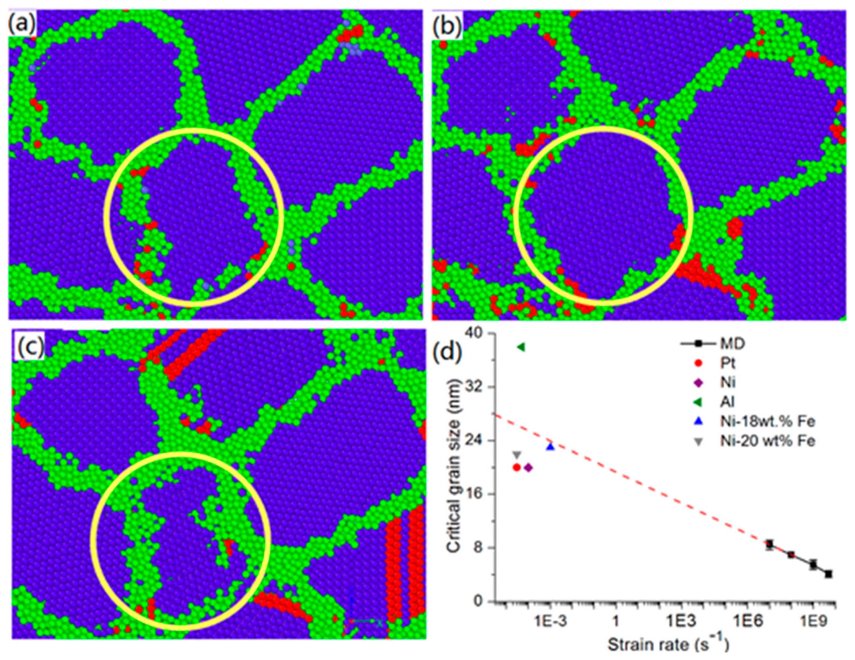
In NC metals, the large amounts of GBs due to the small grain size make them unstable. The grain growth (GG) in NC with small grain size is popular at annealing processes, even in rapid annealing [48], such as laser annealing. Besides the GG in high temperatures, it is also possible for GG to appear at low temperatures [49], especially at the deformation processes [50]. Thus, it has an influence on the mechanical properties of NC. In the processes of deformation, the local shear strain induced by applied tensile strain will facilitate the grain coalescence [38]. In Figure S4, the initial atomic structure and that under the strain of 4.5% with strain rate of 5 ns−1 for NC gold with grain size of 3.8 nm are shown. As per the circles in Figure S4a,b, the configurations of GBs are modulated due to the realignment of atoms at GBs under the local stress and thus the size of the grain changes, accompanied by the stacking faults emission through grain interior.
We have noticed that the atomic realignment at GBs leads to the change of grain size in the processes of tensile strain. We have analyzed statistically the distribution of grain size at different strains by the methods mentioned above. We used the NC gold with average grain sizes of 3.8 nm and 4.5 nm under applied strain with a strain rate of 5 ns−1 as examples. We checked the change of the ten largest grains in the simulated cell. It was found that for the sample of average grain of 3.8 nm under the strain of 4.5%, the sizes of the three largest grains increase from 5.67, 5.07 and 4.79 nm in initial the structure to 5.83, 5.58 and 5.34 nm, respectively. Clearly, the three largest grains have been grown significantly relative to the initial structure, accompanied by decrease of other smaller grains, like the Ostwald ripening. Interestingly, in the NC gold of 4.5 nm with strain rate of 5 ns−1, it isn’t found that the grains grow up.
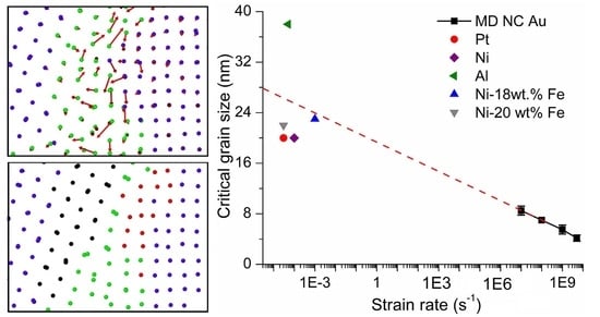
In Figure 7a–c, we show the atomic configurations of 6 nm NC gold under the tensile strain of 7% with the strain rate of 0.1 ns−1 and 1 ns−1. It can find that the grain grows up under a strain rate of 0.1 ns−1 and doesn’t grow under a strain rate of 1 ns−1, as indicated by the circles in Figure 7b,c. Thus, it is proposed that there is a critical grain size for each strain rate. Under a fixed strain rate, it is possible to make the GG appear when grain size is less than the corresponding critical grain size. We analyzed the critical grain size by the statistical method of grain size mentioned above for the cases of different initial grain sizes under different strain rates. The details are listed in Figures S5–S8. In Figure 7d, we show the relation of critical grain size and strain rate. We found that the critical grain size became large, by following the decrease of strain rate. By the extrapolation, we can propose the critical grain size is about 25 nm under the strain rate of 10−4 s−1 (which is the regular strain rate used in experiments) if the main mechanism of GG isn’t changed. This is consistent with the previous observations in experiments about other NC metals [51,52,53,54,55]. For example, in NC Pt thin film, the GG appears with grain sizes for a dozen, even tens of, nanometers during the tensile deformation test under a strain rate of 3 × 10⁻⁵ s−1.
For the GG during the tensile strain, the change of GBs’ configuration is an important way as mentioned above. One of the important mechanisms is grain rotation, in which the dependence of GB’s energy on misorientation between two nearby grains is the driving force. The local shear stress will rotate the grain to form low energetic GBs, as indicated by the previous simulations [38,56]. Generally, the GB migration and grain rotation derived by the local large stress near GBs with the assistance of dislocation take the main rule. Thus, the growth up of single grain or/and the coalescence between grains to form a larger grain appear in the tensile deformation processes. As an example, the coalescence between grains in 7 nm NC gold under tensile strain is shown in Figure S9.
4. Conclusions
We have explored the effect of strain rate on the elasticity, plastic deformation and grain growth of NC gold with small grain size by using molecular dynamics simulations. By considering the models of NC gold with grain sizes of 6 nm and 18 nm, we found that that the apparent Young’s modulus of NC gold decreases by following the strain rate decreases. By comparing with that of single crystalline and amorphous gold, it was found that this couldbe attributed to the decrease of effective Young’s modulus from GBs with the decrease of strain rate. It was noticed that under a low strain rate of less than 0.5 per ns, the value of apparent Young’s modulus of amorphous gold oscillates around 3.19 GPa. The GBs had similar atomic arrangements to amorphous structure and thus small effective Young’s modulus under low strain rate. Thus, by following the decrease of grain size the apparent Young’s modulus of NC decreased due to the contribution of larger atomic fraction of GBs. The low apparent Young’s modulus at low strain was due to the atomic rearrangement around GBs even under small applied tensile strain.
For the response of NC gold to strain rate, flow stress has similar laws to apparent Young’s modulus. Following the decrease of strain rates of less than 1 per ns, the decrease of flow stress became slow, especially for larger grain size (such as 18 nm). From the relation between flow stress and strain rate, we found that strain rate sensitivity decreased and activation volume increased with the increase of strain rate. The larger the grain size, the quicker the decrease of strain rate sensitivity. Thus, under lower strain rate, the strain rate sensitivity of larger grain size was smaller. When the strain rate was below 0.1 per ns, the strain rate sensitivities of 18 nm NC gold was just 0.016. Temperature had little effect on the strain rate sensitivity and thus activation volume of 6 nm NC gold. However, there was an obvious effect on NC gold with a grain size of 18 nm. We found that the activation volume of 18 nm NC at 300 K was about 18.69 b3 under a strain rate of 0.01 ns−1. This indicates that the larger flow stress of 18 nm NC is due to the dislocation pile-up against GBs as the main deformation mechanism under applied strain. For the smaller grain size (such as 6 nm) and high temperature, the smaller activation volume is due to GB slipping and/or change of atomic configuration near GBs. We found that grain growth in NC was related to strain rate in the process of tensile strain. There is a critical grain size about grain growth for each strain rate and the critical grain size increases by following the decrease of strain rate. We propose the critical size for grain growth is about 25 nm under the strain state used in the usual experiments.
Supplementary Materials
The following are available online at https://www.mdpi.com/2073-4352/10/10/858/s1, Figure S1: both modes of amorphous gold, Figure S2: Strain-stress curves of 6 nm and 18 nm grain sizes under different strain rates, Figure S3: The loading and unloading processes for the case of grain size of 6 nm, Figure S4: Atomic configurations of 3.8 nm grain size under strains, Figures S5–S8: analysis of critical size for grain growth, Figure S9: atomic configuration of 7 nm grain size.
Author Contributions
Conceptualization, X.F. and W.Z.; methodology, X.F.; software, J.L.; validation, X.F., J.L., Y.S., and D.J.S.; formal analysis, X.F., J.L.; investigation, X.F., J.L.; resources, X.F.; data curation, X.F., J.L.; writing—original draft preparation, J.L.; writing—review and editing, X.F., Y.S., D.J.S., W.Z.; visualization, J.L., X.F.; supervision, X.F.; project administration, X.F.; funding acquisition, X.F., W.Z. All authors have read and agreed to the published version of the manuscript.
Funding
This research was funded by the National Key R&D Program of China, grant number 2016YFA0200400, and the National Natural Science Foundation of China, grant number 51627805. The APC was funded by the National Key R&D Program of China.
Conflicts of Interest
The authors declare no conflict of interest.
References
- Youssef, K.M.; Scattergood, R.O.; Murty, K.L. Ultrahigh strength and high ductility of bulk nanocrystalline copper. Appl. Phys. Lett. 2005, 87, 091904. [Google Scholar] [CrossRef]
- Zhang, M.; Yang, B.; Chu, J.; Nieh, T.G. Hardness enhancement in nanocrystalline tantalum thin films. Scr. Mater. 2006, 54, 1227–1230. [Google Scholar] [CrossRef]
- Schuh, C.A.; Nieh, T.G.; Yamasaki, T. Hall–Petch breakdown manifested in abrasive wear resistance of nanocrystalline nickel. Scr. Mater. 2002, 46, 735–740. [Google Scholar] [CrossRef]
- Pande, C.S.; Cooper, K.P. Nanomechanics of Hall–Petch relationship in nanocrystalline materials. Prog. Mater Sci. 2009, 54, 689–706. [Google Scholar] [CrossRef]
- Armstrong, R.W. 60 years of Hall-Petch: Past to present nano-scale connections. Mater. Trans. 2014, 55, 2–12. [Google Scholar] [CrossRef] [Green Version]
- Dao, M.; Lu, L.; Asaro, R.J.; Hosson, J.T.M.D.; Ma, E. Toward a quantitative understanding of mechanical behavior of nanocrystalline metals. Acta Mater. 2007, 55, 4041–4065. [Google Scholar] [CrossRef] [Green Version]
- Yamakov, V.; Wolf, D.; Phillpot, S.R.; Mukherjee, A.K.; Gleiter, H. Deformation-mechanism map for nanocrystalline metals by molecular-dynamics simulation. Nat. Mater. 2004, 3, 43–47. [Google Scholar] [CrossRef]
- Li, H.; Choo, H.; Ren, Y.; Saleh, T.A.; Lienert, U.; Liaw, P.K.; Ebrahimi, F. Strain-dependent deformation behavior in nanocrystalline metals. Phys. Rev. Lett. 2008, 101, 015502. [Google Scholar] [CrossRef] [PubMed]
- Schiøtz, J.; Jacobsen, K.W. A maximum in the strength of nanocrystalline copper. Science 2003, 301, 1357–1359. [Google Scholar] [CrossRef] [PubMed] [Green Version]
- Wang, Y.M.; Hamza, A.V.; Ma, E. Temperature-dependent strain rate sensitivity and activation volume of nanocrystalline Ni. Acta Mater. 2006, 54, 2715–2726. [Google Scholar] [CrossRef]
- Renk, O.; Maier-Kiener, V.; Issa, I.; Li, J.H.; Kiener, D.; Pippan, R. Anneal hardening and elevated temperature strain rate sensitivity of nanostructured metals: Their relation to intergranular dislocation accommodation. Acta Mater. 2019, 165, 409–419. [Google Scholar] [CrossRef]
- Huang, P.; Wang, F.; Xu, M.; Xu, K.W.; Lu, T.J. Dependence of strain rate sensitivity upon deformed microstructures in nanocrystalline Cu. Acta Mater. 2010, 58, 5196–5205. [Google Scholar] [CrossRef]
- Carlton, C.E.; Ferreira, P.J. What is behind the inverse Hall–Petch effect in nanocrystalline materials? Acta Mater. 2007, 55, 3749–3756. [Google Scholar] [CrossRef]
- Chen, J.; Lu, L.; Lu, K. Hardness and strain rate sensitivity of nanocrystalline Cu. Scr. Mater. 2006, 54, 1913–1918. [Google Scholar] [CrossRef]
- Schiøtz, J.; Vegge, T.; Tolla, F.D.D.; Jacobsen, K.W. Atomic-scale simulations of the mechanical deformation of nanocrystalline metals. Phys. Rev. B 1999, 60, 11971. [Google Scholar] [CrossRef] [Green Version]
- Wei, Q.; Cheng, S.; Ramesh, K.T.; Ma, E. Effect of nanocrystalline and ultrafine grain sizes on the strain rate sensitivity and activation volume: Fcc versus bcc metals. Mater. Sci. Eng. A 2004, 381, 71–79. [Google Scholar] [CrossRef]
- Asaro, R.J.; Suresh, S. Mechanistic models for the activation volume and rate sensitivity in metals with nanocrystalline grains and nano-scale twins. Acta Mater. 2005, 53, 3369–3382. [Google Scholar] [CrossRef]
- Kanel, G.I.; Zaretsky, E.B.; Razorenov, S.V.; Ashitkov, S.I.; Fortov, V.E. Unusual plasticity and strength of metals at ultra-short load durations. Phys. Uspekhi 2017, 60, 490. [Google Scholar] [CrossRef] [Green Version]
- Chen, A.Y.; Ruan, H.H.; Wang, J.; Chan, H.L.; Wang, Q.; Li, Q.; Lu, J. The influence of strain rate on the microstructure transition of 304 stainless steel. Acta Mater. 2011, 59, 3697–3709. [Google Scholar] [CrossRef]
- Jonnalagadda, K.N.; Chasiotis, I.; Yagnamurthy, S.; Lambros, J.; Pulskamp, J.; Polcawich, R.; Dubey, M. Experimental investigation of strain rate dependence of nanocrystalline Pt films. Exp. Mech. 2010, 50, 25–35. [Google Scholar] [CrossRef]
- Karanjgaokar, N.J.; Oh, C.-S.; Lambros, J.; Chasiotis, I. Inelastic deformation of nanocrystalline Au thin films as a function of temperature and strain rate. Acta Mater. 2012, 60, 5352–5361. [Google Scholar] [CrossRef]
- Lu, L.; Li, S.X.; Lu, K. An abnormal strain rate effect on tensile behavior in nanocrystalline copper. Scr. Mater. 2001, 45, 1163–1169. [Google Scholar] [CrossRef]
- Schwaiger, R.; Moser, B.; Dao, M.; Chollacoop, N.; Suresh, S. Some critical experiments on the strain-rate sensitivity of nanocrystalline nickel. Acta Mater. 2003, 51, 5159–5172. [Google Scholar]
- Lu, L.; Schwaiger, R.; Shan, Z.W.; Dao, M.; Lu, K.; Suresh, S. Nano-sized twins induce high rate sensitivity of flow stress in pure copper. Acta Mater. 2005, 53, 2169–2179. [Google Scholar]
- Lu, L.; Shen, Y.; Chen, X.; Qian, L.; Lu, K. Ultrahigh strength and high electrical conductivity in copper. Science 2004, 304, 422–426. [Google Scholar] [CrossRef] [PubMed] [Green Version]
- Rida, A.; Micoulaut, M.; Rouhaud, E.; Makke, A. Understanding the strain rate sensitivity of nanocrystalline copper using molecular dynamics simulations. Comp. Mater. Sci. 2020, 172, 109294. [Google Scholar]
- Jonnalagadda, K.; Karanjgaokar, N.; Chasiotis, I.; Chee, J.; Peroulis, D. Strain rate sensitivity of nanocrystalline Au films at room temperature. Acta Mater. 2010, 58, 4674–4684. [Google Scholar]
- Zhang, T.; Zhou, K.; Chen, Z.Q. Strain rate effect on plastic deformation of nanocrystalline copper investigated by molecular dynamics. Mater. Sci. Eng. A 2015, 648, 23–30. [Google Scholar]
- Yaghoobi, M.; Voyiadjis, G.Z. The effects of temperature and strain rate in fcc and bcc metals during extreme deformation rates. Acta Mater. 2018, 151, 1–10. [Google Scholar] [CrossRef]
- Rupert, T. Strain localization in a nanocrystalline metal: Atomic mechanisms and the effect of testing conditions. J. Appl. Phys. 2013, 114, 033527. [Google Scholar]
- Zhou, K.; Liu, B.; Yao, Y.; Zhong, K. Grain coarsening in nanocrystalline copper with very small grain size during tensile deformation. Mater. Sci. Eng. A 2014, 595, 118–123. [Google Scholar] [CrossRef]
- Plimpton, S. Fast parallel algorithms for short-range molecular dynamics. J. Comput. Phys. 1995, 117, 1–19. [Google Scholar] [CrossRef] [Green Version]
- Foiles, S.M.; Baskes, M.I.; Daw, M.S. Embedded-atom-method functions for the fcc metals Cu, Ag, Au, Ni, Pd, Pt, and their alloys. Phys. Rev. B 1986, 33, 7983. [Google Scholar] [CrossRef] [PubMed]
- Hirel, P. Atomsk: A tool for manipulating and converting atomic data files. Comput. Phys. Commun. 2015, 197, 212–219. [Google Scholar] [CrossRef]
- Stukowski, A. Visualization and analysis of atomistic simulation data with OVITO—The Open Visualization Tool. Model. Simul. Mater. Sci. Eng. 2009, 18, 015012. [Google Scholar] [CrossRef]
- Stukowski, A.; Bulato, V.V.; Arsenlis, A. Automated identification and indexing of dislocations in crystal interfaces. Model. Simul. Mater. Sci. Eng. 2012, 20, 085007. [Google Scholar] [CrossRef]
- Stukowski, A. Computational analysis methods in atomistic modeling of crystals. JOM 2014, 66, 399–407. [Google Scholar] [CrossRef]
- Liu, J.; Fan, X.; Zheng, W.; Singh, D.J.; Shi, Y. Nanocrystalline gold with small size: Inverse Hall–Petch between mixed regime and super-soft regime. Philos. Mag. 2020, 100, 2335–2351. [Google Scholar] [CrossRef]
- Liu, J.; Fan, X.; Shi, Y.; Singh, D.J.; Zheng, W. Nanopores in nanocrystalline gold. Materialia 2019, 5, 100195. [Google Scholar] [CrossRef]
- Fougere, G.E.; Riester, L.; Ferber, M.; Weertman, J.R.; Siegel, R.W. Young’s modulus of nanocrystalline Fe measured by nanoindentation. Mater. Sci. Eng. A 1995, 204, 1–6. [Google Scholar] [CrossRef]
- Sanders, P.G.; Eastman, J.A.; Weertman, J.R. Elastic and tensile behavior of nanocrystalline copper and palladium. Acta Mater. 1997, 45, 4019–4025. [Google Scholar] [CrossRef]
- Sharma, P.; Ganti, S. On the grain-size-dependent elastic modulus of nanocrystalline materials with and without grain-boundary sliding. J. Mater. Res. 2003, 18, 1823–1826. [Google Scholar] [CrossRef]
- Wang, Y.M.; Ma, E. Strain hardening, strain rate sensitivity, and ductility of nanostructured metals. Mater. Sci. Eng. A 2004, 375, 46–52. [Google Scholar] [CrossRef]
- Petegem, S.V.; Brandstetter, S.; Schmitt, B.; Swygenhoven, H.V. Creep in nanocrystalline Ni during X-ray diffraction. Scr. Mater. 2009, 60, 297–300. [Google Scholar]
- Kottada, R.S.; Chokshi, A.H. Low temperature compressive creep in electrodeposited nanocrystalline nickel. Scr. Mater. 2005, 53, 887–892. [Google Scholar] [CrossRef] [Green Version]
- Chokshi, A.H. Unusual stress and grain size dependence for creep in nanocrystalline materials. Scr. Mater. 2009, 61, 96–99. [Google Scholar] [CrossRef]
- Ma, E. Watching the nanograins roll. Science 2004, 305, 623–624. [Google Scholar] [CrossRef] [PubMed]
- Liu, J.; Fan, X.; Shi, Y.; Singh, D.J.; Zheng, W. Melting of nanocrystalline gold. J. Phys. Chem. C 2018, 123, 907–914. [Google Scholar] [CrossRef]
- Rösner, H.; Markmann, J.; Weissmüller, J. Deformation twinning in nanocrystalline Pd. Philos. Mag. Lett. 2004, 84, 321–334. [Google Scholar] [CrossRef]
- Haslam, A.J.; Moldovan, D.; Yamakov, V.; Wolf, D.; Phillpot, S.R.; Gleiter, H. Stress-enhanced grain growth in a nanocrystalline material by molecular-dynamics simulation. Acta Mater. 2003, 51, 2097–2112. [Google Scholar] [CrossRef]
- Fan, G.J.; Fu, L.F.; Choo, H.; Liaw, P.K.; Browning, N.D. Uniaxial tensile plastic deformation and grain growth of bulk nanocrystalline alloys. Acta Mater. 2006, 54, 4781–4792. [Google Scholar]
- Sharon, J.A.; Su, P.-C.; Prinz, F.B.; Hemker, K.J. Stress-driven grain growth in nanocrystalline Pt thin films. Scr. Mater. 2011, 64, 25–28. [Google Scholar]
- Gianola, D.S.; Petegem, S.V.; Legros, M.; Brandstetter, S.; Swygenhoven, H.V.; Hemker, K.J. Stress-assisted discontinuous grain growth and its effect on the deformation behavior of nanocrystalline aluminum thin films. Acta Mater. 2006, 54, 2253–2263. [Google Scholar]
- Wang, Y.B.; Li, B.Q.; Sui, M.L. Deformation-induced grain rotation and growth in nanocrystalline Ni. Appl. Phys. Lett. 2008, 92, 011903. [Google Scholar]
- Wang, Y.B.; Ho, J.C.; Liao, X.Z.; Li, H.Q.; Ringer, S.P.; Zhu, Y.T. Mechanism of grain growth during severe plastic deformation of a nanocrystalline Ni–Fe alloy. Appl. Phys. Lett. 2009, 94, 011908. [Google Scholar]
- Sansoz, F.; Dupont, V. Grain growth behavior at absolute zero during nanocrystalline metal indentation. Appl. Phys. Lett. 2006, 89, 111901. [Google Scholar]
Figure 1.
Atomic configurations of nanocrystalline gold samples with mean grain sizes of (a) 6 nm and (b) 18 nm. Blue and green represent grain interiors with fcc lattice and atoms at grain boundaries, respectively.
Figure 1.
Atomic configurations of nanocrystalline gold samples with mean grain sizes of (a) 6 nm and (b) 18 nm. Blue and green represent grain interiors with fcc lattice and atoms at grain boundaries, respectively.
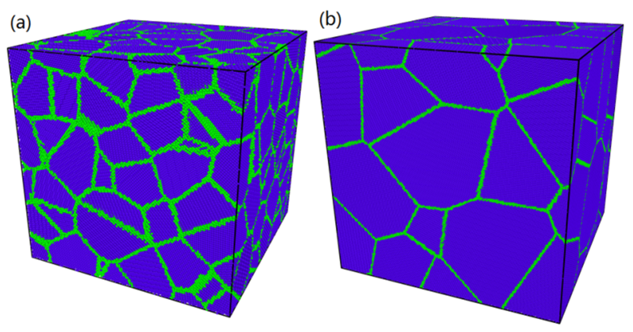
Figure 2.
(a) Stress-strain curves for nanocrystalline gold simulations with grain size of 6 nm under different strain rates from 0.01 ns−1 to 10 ns−1; and (b) Young’s modulus as the function of strain rate for amorphous gold with two models (Amorphous, NC-1 nm), nanocrystalline gold with a grain size of 6 nm (NC-6 nm-m1 from strain–stress method, NC-6 nm-m2 from method 2 mentioned in the text), and grain size of 18 nm (NC-18 nm-m1, NC-18 nm-m2) and single crystal under strain long [100] direction (SC-[100]-m1, SC-[100]-m2) and [111] directions (SC-[111]-m1, SC-[111]-m2).
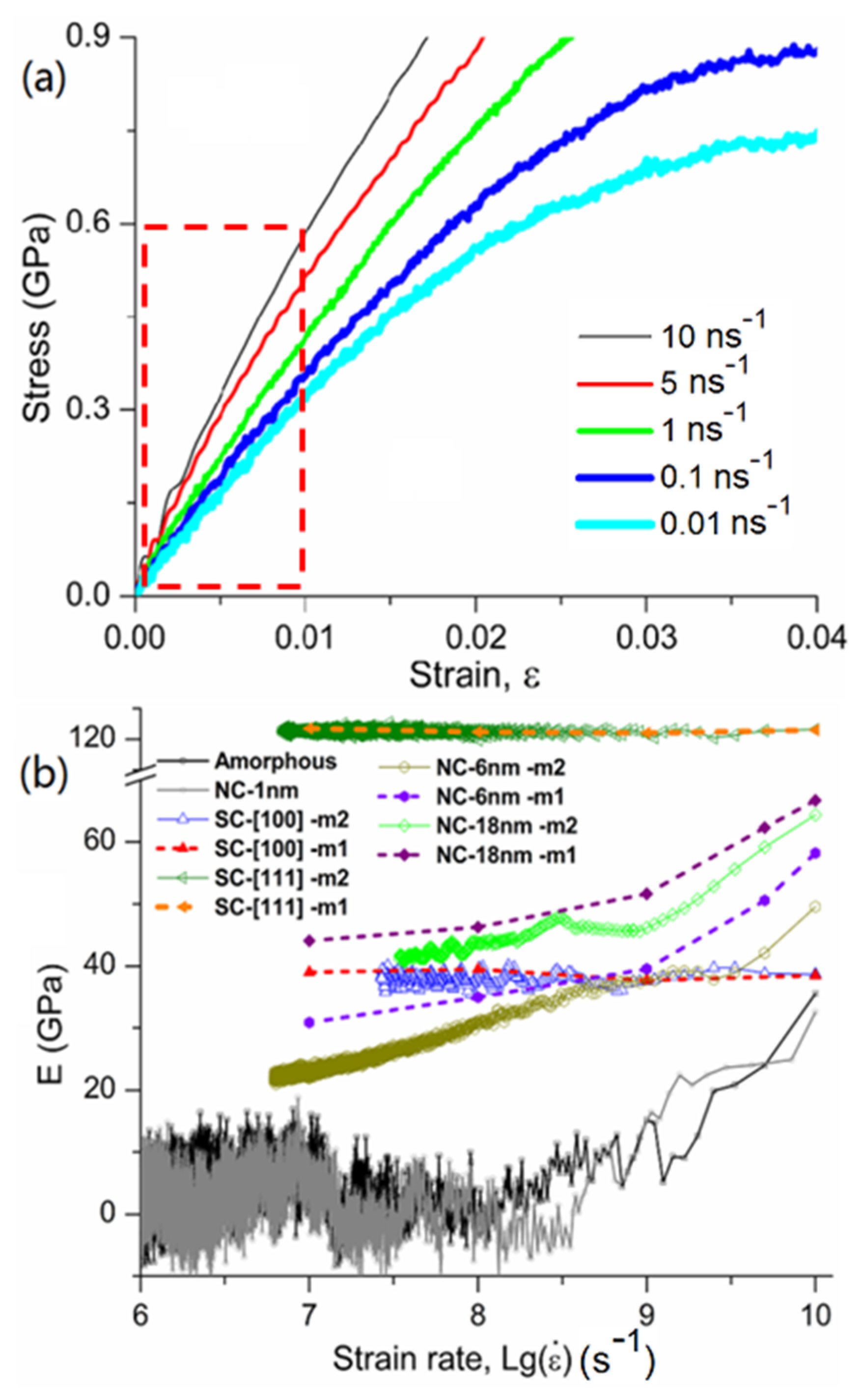
Figure 3.
(a) Atomic configuration of grain size of 6 nm after a strain of 1% in 0.1 ps (blue and green represent grain interiors with fcc and atoms at grain boundaries, respectively); (b) atomic configuration after the structural relaxation of 850 ps under a strain of 1% whose initial structure is the structure in (a); and (c) distribution of atomic weight as a function of atomic displacement for grain size of 6 nm under stain of 1% (the structure in (a) is the initial structure) at different relaxation times. In (a), the red arrows in each atom represent the displacement size of atoms from the initial structure to the configuration after the relaxation of 850 ps under a strain of 1%. In (b), the black represents the atoms of grain interiors with fcc whose initial positions are disordered and belong to grain boundaries, and the red represents the atoms of grain boundaries whose initial positions are ordered with fcc and belong to grain interiors in (a).
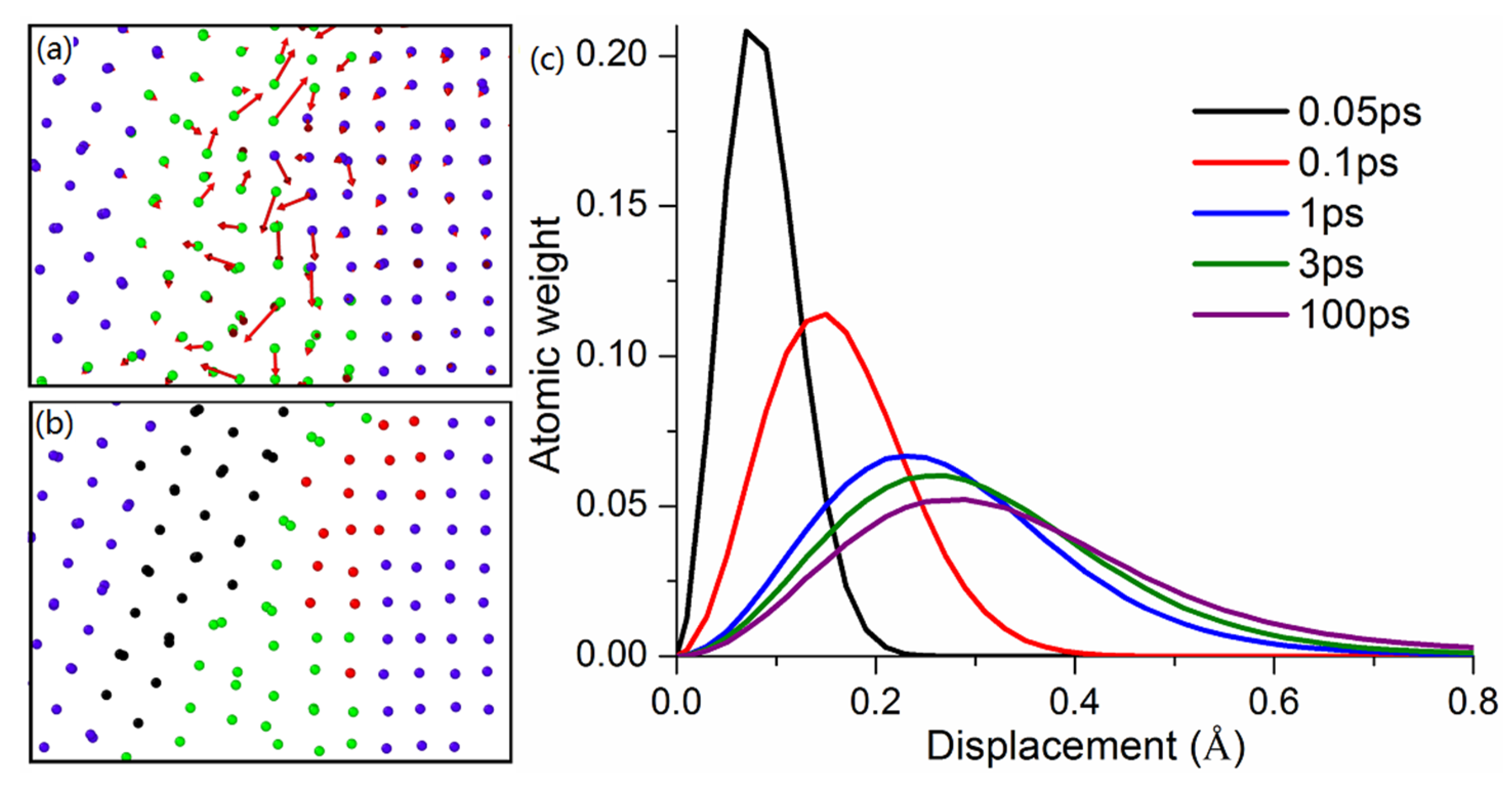
Figure 4.
(a) Stress and dislocation density as functions of tensile strain for nanocrystalline gold of 6 nm grain size and 18 nm grain size at a strain rate of 1 ns−1; (b) flow stress; (c) strain rate sensitivity as functions of strain rate for nanocrystalline gold; and (d) dislocation densities as a function of tensile strain for grain size of 6 nm under different strain rate.

Figure 5.
Atomic configurations and distribution of local shear strain of grain size of 6 nm at tensile strain of 4% under the strain rate of (a,b) 0.1 ns−1 and (e,f) 10 ns−1, and that at tensile strain 10% under the strain rate of (c,d) 0.1 ns−1 and (g,h) 10 ns−1. In (a,c,e,g), blue, red and green represent grain interiors with fcc, stacking faults with hcp, and atoms at grain boundaries, respectively. In (b,d,f,h), the change of color from blue to red indicates the increase of atomic local shear strain.
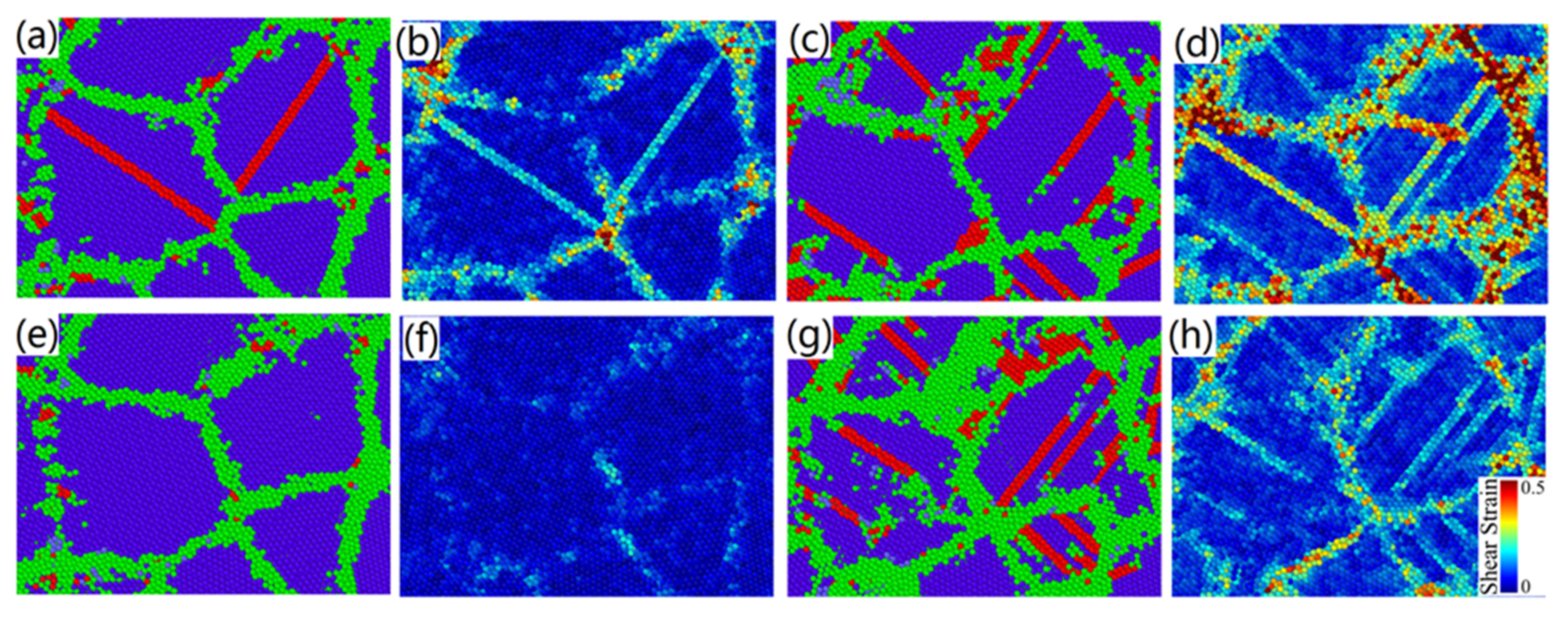
Figure 6.
(a) Stress–strain curves for nanocrystalline gold with grain sizes of 6 nm and 18 nm with a strain rate of 1 ns−1 with 300 K and 800 K, (b) flow stress and (c) activation volume as functions of strain rate for grain sizes of 6 nm and 18 nm with 300 K and 800 K, and (d) the distribution of atomic weight as a function of atomic shear strain for 18 nm grain size with 300 K and 6 nm grain size with 600 K and 600 K at tensile strain 7.5% under the strain rates of 0.01 ns−1.
Figure 7.
(a) The initial structures of grain size of 6 nm, atomic configurations of it at tensile strain of 7% under the stain rate of (b) 0.1 ns−1 and (c) 1 ns−1, and (d) critical grain size for grain growth as a function of strain rate. In (a–c), blue, red and green represent grain interiors with fcc, stacking faults with hcp, and atoms at grain boundaries, respectively. In (d) experimental results from [46,47,48,49,50] are provided for comparison.
© 2020 by the authors. Licensee MDPI, Basel, Switzerland. This article is an open access article distributed under the terms and conditions of the Creative Commons Attribution (CC BY) license (http://creativecommons.org/licenses/by/4.0/).
Share and Cite
MDPI and ACS Style
Liu, J.; Fan, X.; Shi, Y.; Singh, D.J.; Zheng, W. The Effect of Strain Rate on the Deformation Processes of NC Gold with Small Grain Size. Crystals 2020, 10, 858. https://doi.org/10.3390/cryst10100858
AMA Style
Liu J, Fan X, Shi Y, Singh DJ, Zheng W. The Effect of Strain Rate on the Deformation Processes of NC Gold with Small Grain Size. Crystals. 2020; 10(10):858. https://doi.org/10.3390/cryst10100858
Chicago/Turabian StyleLiu, Jialin, Xiaofeng Fan, Yunfeng Shi, David J. Singh, and Weitao Zheng. 2020. "The Effect of Strain Rate on the Deformation Processes of NC Gold with Small Grain Size" Crystals 10, no. 10: 858. https://doi.org/10.3390/cryst10100858
Note that from the first issue of 2016, this journal uses article numbers instead of page numbers. See further details here.