Abstract
Self-assembled strategy has been proven to be a promising vista in constructing organized low-dimensional nanostructures with molecular precision and versatile functionalities on solid surfaces. Herein, we investigate by a combination of scanning tunneling microscopy (STM) and dispersion-corrected density functional theory (DFT), the adsorption of tetracene molecules on the silver substrate and the mechanism mediating the self-assembly on Ag(110). As expected, ordered domain is formed on Ag(110) after adsorption with adjacent molecules being imaged with alternating bright or dim pattern regularly. While such behavior has been assigned previously to the difference of molecular adsorption height, herein, it is possible to investigate essentially the mechanism leading to the periodic alternation of brightness and dimness for tetracene adsorbed on Ag(110) thanks to the consideration of Van der Waals (vdW) dispersion force. It is demonstrated that the adsorption height in fact is same for both bright and dim molecules, while the adsorption site and the corresponding interfacial charge transfer play an important role in the formation of such pattern. Our report reveals that vdW dispersion interaction is crucial to appropriately describe the adsorption of tetracene on the silver substrate, and the formation of delicate molecular architectures on metal surfaces might also offers a promising approach towards molecular electronics.
1. Introduction
Organic-inorganic hybrid materials have drawn intensive interests in past decades owing to their attractive applications in organic thin film transistors (OTFT), organic light emitting diodes (OLED), solar cells and so on [1,2,3]. Promoted by the rapid development of molecular electronics, low-dimension artificial architectures consisting of small conjugated molecules have gone through vigorous exploiting [4,5], which in turn offer the possibility to integrate simultaneously the electronic and optoelectronic properties of functional nanostructures into a single device. In practice, such devices are typically constructed in the form of layered structures with metal electrodes, the electron/hole transporting layer and functional organic films in between. Specifically, it is widely perceived that metal/organic interfaces in devices are critical which determine the performance of related devices [3,6]. Therefore, fundamental understanding at the atomic/molecular level is crucial for stimulated promotion and widespread application of molecular electronics, for instance, regarding on fabricating functional organic films and engineering metal/organic interfaces towards the excellent carrier mobility, tunable and so on [7,8].
Consequently, numerous studies have therefore been devoted to fabricating functional organics on solid substrates with the specific attention focused on planar molecules such as aromatics [9]. In particular, tetracene has been proven to be an appealing candidate due to its low-cost processability, high stability, and appropriate band gap [1,10]. Therefore, considerable investigations have been paid to the preparation of tetracene film on solid substrates [11,12,13,14,15,16,17,18,19,20,21,22]. For example, the adsorption of tetracene molecules on the silver substrate has been exploited in literature via scanning tunneling microscopy (STM) [23,24], ultraviolet photoemission spectroscopy (UPS) [25] and so on. It has been discovered that tetracene is adsorbed with the molecular plane parallel to the silver substrate in most cases. In addition, tetracene can also be packed with varying manners depending on the film thickness, for instance, the long molecular axis of tetracene can be aligned along either the [001] or [1,2,3,4,5,6,7,8,9,10] symmetry direction of Ag(110). In special, it was demonstrated that neighboring tetracene molecules were imaged with alternating bright and dim area in STM with high molecular coverage in dense packing in our previous work [16], which was originally assigned to the adsorption height difference induced by the delicate balance between the molecule-substrate and intermolecular interaction, as pointed out by conventional density functional theory (DFT) calculations. However, it has been realized afterwards that, however, the commonly used exchange-correlation functions for electrons, either local density approximation (LDA) or extensions thereof, gradient approximation (GGA) fail to describe the long-range electron correlations (or electron dispersion force) [26,27], namely, the Van der Waals (vdW) interaction, which is found to play a core role in determining the structure and properties of noncovalent or weak bonding molecular network [28].
Attributed to the rapid and expanding development of DFT, especially the introduction of van der Waals interaction correction [26,27,28], noncovalent forces such as hydrogen bonding and vdW interactions can be much more accurately described in supramolecular architectures, molecular crystals, adsorbates and solids nowadays [29,30,31,32]. Based on these considerations, the lack of vdW interaction description in the tetracene/Ag(110) adsorption complex might give unreliable explanation to STM observations in the previous work [16]. Therefore, it becomes meaningful to reinvestigate the tetracene molecular network formed on the Ag(110) surface via the dispersion-corrected DFT approach, which might shed new insights onto understanding the adsorption mechanism behind such interesting arrangement of tetracene molecules. Moreover, electronic structures of the tetracene/Ag(110) interface with the periodic alternation of brightness can also be accurately explored, which hasn’t been addressed before. As a result, herein, a dedicated investigation of the tetracene molecule adsorbed on the Ag(110) substrate has been carried out utilizing the vdW-interaction-corrected DFT approach together with STM measurements. By investigating the charge density and density of states at interface, as well as comparing STM simulations to STM results in succession, it is possible to clearly identify the contribution from vdW dispersion interaction to the ultimate formation of the well-defined domain with alternating brightness and dimness, and demonstrate the key role of adsorption site of tetracene on Ag(110) instead of the adsorption height difference.
2. Materials and Methods
STM experiments were performed in an ultrahigh-vacuum (UHV) variable temperature STM system (VT-STM, Omicron, Berlin, Germany) with a base pressure better than 5.0 × 10⁻¹⁰ mbar, details can be found elsewhere [16,33]. The clean Ag(110) surface (Mateck) was obtained by cycles of argon sputtering (1200 V at beginning and 800 eV in the end) and post annealing to around 573 K, while the cleanliness was double checked by low energy electron diffraction (LEED), core level photoelectron spectroscopy (Specs 100 spectrometer, Berlin, Germany) and STM measurements (Omicron VT-STM). Tetracene (99.99%, Sigma-Aldrich, Buchs, Switzerland) was degassed for several hours before deposition just below sublimation temperature (about 410 K) in a home-made evaporator from Ta foil. Deposition rate was monitored using a quartz microbalance (Omnivac, Kaiserslautern, Germany) and calibrated afterwards with STM measurements, which was about 0.2 ML/min. STM measurements were performed at room temperature (RT).
DFT calculations were performed by employing the Vienna ab initio Simulation Package (VASP) code [34,35,36] with the projector augmented wave (PAW) method [37]. The Perdew-Burke-Ernzerhof (PBE) form within the generalized gradient approximation (GGA) [38] was used to describe the electron exchange-correlation potential. In addition, the DFT-D3 method [39] proposed by Grimme was also adopted to give a better description of the long-range dispersion interactions. The Ag(110) supercell was constructed with a dimension of 15.01 Å × 30.02 Å × 21.0 Å to simulate the unit cell of the adsorption model, including three layers of Ag(110) and four tetracene molecules, and the supercell is consisted of 228 Ag atoms. A vacuum layer of 15 Å was built to prevent interactions between neighboring slabs. The Monkhorst-Pack [40] k-point sampling was utilized for Brillouin zone integration: 3 × 2 × 1. The kinetic energy cutoff for the plane-wave basis was set to 400 eV. During structural optimization, the top two layers and molecules were fully relaxed with a force convergence criterion of 0.02 eV/Å. Simulated STM topography ws created from the partial local density of states by using the Tersoff–Hamann method [41]. Under the present setup, the lattice parameter of the Ag slab was calculated as 4.113 Å, in good agreement with the experimental value of 4.085 Å [42].
3. Results and Discussion
The molecular structure of tetracene is shown in Figure 1 together with the STM simulation in gas phase, and it is found that the electron density distribution of tetracene is strongly dependent on energy, say, the distribution of electron is symmetric with respect to the long molecular axis at positive bias (above the Fermi level) while it has the mirror plane along the short molecular axis at negative bias (below the Fermi level), which is consistent with reports in literature [17,18]. It was revealed that deposition of about one monolayer (ML) tetracene onto Ag(110) kept at room temperature (RT) leads to the formation of a commensurate domain with respect to the Ag substrate, as shown in Figure 2a. Detailed analysis reveals that the long molecular axis of tetracene is aligned with a certain angle respect to the [001] direction from the Ag(110) substrate. While a rhombic unit cell can be extracted for the close packed domain from STM topography in Figure 2a, it is also apparent that the ordered nanostructure with long-range neatness is composed of periodically altering patterns with the bright or dim tetracene as predicated by STM simulations under positive bias in Figure 1. With two neighboring molecules imaged with relative brightness and dimness around the [001] symmetry direction of substrate, a zoom-in view in Figure 2b also shows that even the two bright tetracene molecules within the same unit cell is slightly different from STM topography. Specifically, one tetracene molecule is completely bright in STM, while another tetracene at the diagonal position is found to be imaged as half bright and half dim, which are highlighted by the yellow ellipses in Figure 2b. This observation is kind of interesting and hasn’t been discussed yet in previous reports, and the governing mechanism underneath might be related to the adsorption site at a first sight.
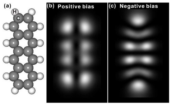
Figure 1.
(a) A schematic drawing of tetracene. Grey: carbon; White, hydrogen; (b) STM simulation of tetracene in gas phase under positive bias; (c) STM simulation of tetracene of gas-phase tetracene under negative bias.
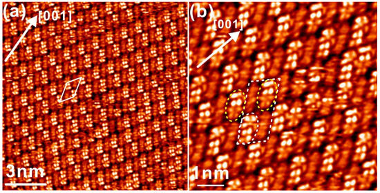
Figure 2.
(a) STM topography of about 1 ML tetracene adsorbed on Ag(110) at RT. (b) The close-up view of the self-assembled tetracene molecules possessing periodically varying molecular brightness. Scanning parameters: bias voltage 1.5 v, tunneling current: 1.0 nA.
In order to gain deep insight onto the adsorption morphology and the governing mechanism, DFT calculations have been employed with the consideration of van der Waals (vdW) interaction to predict the adsorption behavior of tetracene on Ag(110). It has been pointed out by conventional DFT calculations without the long-range vdW interaction correction in our previous work [16] that, the variation of the brightness of individual tetracene molecule was caused by the difference of adsorption height between two neighboring tetracene molecules with respect to the silver substrate, which was found to be 2.75 Å and 3.20 Å, respectively. However, different adsorption configurations are obtained herein when the vdW dispersion force is considered. Indeed, the long-range electron dispersion force might play a key role in the description of the tetracene/Ag(110) adsorption complex, as the molecule-substrate interaction is revealed to be relatively rather weak [20,21,22]. The adsorption configuration with neighboring tetracene at different adsorption heights was adopted as the starting point following our previous work [16] and was fully relaxed afterwards during the vdW-corrected DFT optimization. Finally, optimized adsorption models are summarized and illustrated in Figure 3 with both top and side view shown. It can be seen that tetracene molecules can be arranged with two slightly different adsorption sites in the same unit cell, as marked by the white and red ellipse in Figure 3a,b, respectively. While one tetracene molecule corresponding to the bright feature in STM is positioned with the molecular backbone on the top site (indicated with the white ellipse in Figure 3a), another bright molecule can either park on the top site as well or be arranged with the molecular backbone on the long bridge site (red ellipse in Figure 3b). Further analysis in detail gives the unit cell parameter for the first adsorption configurations as:
where a and b indicate the unit cell vector of the assembled nanostructure, and as and bs represent the unit cell vector of the Ag(110) substrate, while the 2nd configuration does not compensate with the Ag(110) substrate and might not be possible to be observed experimentally [43].
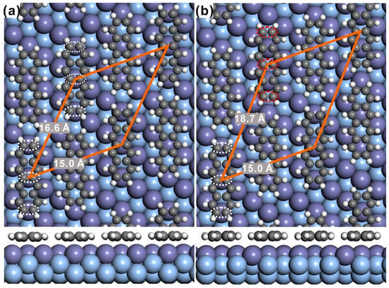
Figure 3.
Predicted adsorption models for the tetracene/Ag(110) interface as acquired from the vdW-corrected DFT approach. For easy illustration, both top and side views are presented. (a,b) are the two stable configurations from calculations, in which the unit cell is highlighted by the orange rhomb with the length of vectors marked, and the molecular backbone is indicated by white dashed ellipse.
Interestingly, the adsorption height of neighboring tetracene molecules is almost identical as seen from the side-view configuration at the bottom in Figure 3, which is predicted by the vdW corrected DFT calculations. Apparently, such prediction is different from the conclusion in previous work [16], where the adsorption height of adjacent tetracene molecules was expected to be different resulting in the alternating-brightness feature of tetracene adsorbed on Ag(110). Therefore, the vdW dispersion is supposed to play an import role in mediating the formation of the varying-brightness pattern for self-assembled tetracene molecules on Ag(110). Under the predication that the adsorption height is same for all tetracene molecules on the silver substrate, the appearance of periodically varied brightness in STM might then be related to the adsorption site, which has been revealed to in general induce the variation of density of states [44,45] and consequently the corresponding STM imaging. In order to verify this hypothesis, charge density difference (CDD) was then calculated at the tetracene/Ag(110) interface and represented in Figure 4a. Clearly, unidentical CDD is revealed for the four tetracene molecules within one unit cell. Intense CDD indicates strong charge transfer across interface (from Ag atoms to tetracene molecules), leading to relatively high density of states and consequently the appearance of bright feature in STM. On the other hand, less visible CDD at the tetracene/Ag(110) interface might result in the emergence of dim features for the adsorbed tetracene molecules. Further investigation indicates that the difference in CDD can be assigned to the variation of adsorption sites. If the node of the tetracene molecule is placed on top of the surface Ag atom (highlighted by white lines in Figure 4a), apparent CDD is induced and observed. On the contrary, invisible CDD is discovered once molecular nodes are positioned away from the top site, for instance, close to the hollow site as marked by purple lines in Figure 4a. Less charge transfer from the silver substrate to molecules around the hollow site accordingly results in the relative dim appearance for monomers, while strong charge transfer at the top site leads to the appearance of bright feature in STM imaging.
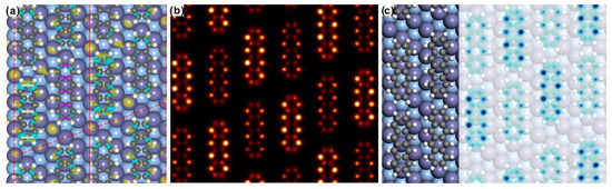
Figure 4.
(a) Calculated charge density difference for the compensated adsorption of tetracene on Ag(110) while molecular nodes are indicated by colored lines. Electron accumulation (depletion) is distinguished by the yellow (cyan) isosurface in the unit of e/Bohr3. (b) The simulated STM topography based on the compensated adsorption configuration shows reasonable agreement with the experimental data. Bias voltage of 0.8 eV was utilized for STM simulation. (c) A hybridized image with the STM simulation overlaid on top of the adsorption configuration for better illustration.
Following the description of CDD, STM simulation has also been performed based on the optimized adsorption configuration and is depicted in Figure 4b. It can be seen that the STM simulation matches quite well with the CDD prediction and is reasonably consistent with the experimental finding, where the relatively bright and dim molecules are packed next to each other in array. To make the illustration clear, Figure 4c shows the STM simulation transparently overlaid on top of the adsorption configuration. Tetracene molecules can now be differentially recognized on Ag(110) with the difference in STM features directly visible. It is also worthy to be pointed out that two adsorption configurations have indeed been predicted with minor difference regarding on the adsorption site of one of bright tetracene molecules, as discussed previously in Figure 3. However, STM simulations based on these two configurations are hard to distinguish but rather seems to be identical, and such behavior might be related to the similar CDD at the tetracene/Ag(110) interface as long as molecular nodes are placed on top of the surface Ag atoms. Nevertheless, besides the good agreement between the experimental observation and STM simulations, there is still a minor point that one tetracene molecule in the unit cell is imaged experimentally as half bright and half dim, while STM simulations in this study are still not be able to represent such behavior yet.
In short, the formation of patterned molecular nanostructures by the adsorption of π-conjugated tetracene molecules on Ag(110) shows a delicate balance between the inter-molecular and molecule-substrate interaction, and the key role of vdW dispersion force within intermolecular interaction in mediating the tetracene molecular network on Ag(110), in good agreement with literature reports of aromatic molecules adsorbed on coinage metal surfaces [30,31,32]. While the periodical brightness variation of molecular feature in STM experiments has been satisfactorily explained with the long-range vdW dispersion interaction properly considered, this study demonstrates that the adsorption site is considerably important at describing the self-assembled tetracene on Ag(110) and shed further insights onto previous reports of molecular self-assembly [16,46,47,48]. More importantly, herein, the fabrication of periodical molecular pattern on solid substrate could be utilized as a constructive approach to prepare functional template or platform for engineering nanostructures towards molecular electronics and nanodevices.
4. Conclusions
In this report, we have elaborately investigated the adsorption of tetracene molecules on Ag(110) via a combination of scanning tunneling microscopy (STM) and dispersion-corrected density functional theory (DFT), and demonstrate the interaction mechanism mediating the self-assembly of tetracene molecules on the silver substrate. Consistent with previous reports, patterned molecular structures is formed upon the adsorption of tetracene on Ag(110) with adjacent molecules being imaged as relatively bright or dim alternatively, and such interesting behavior has been previously explained by the variation at adsorption height of tetracene molecules. Based on this, the essential mechanism leading to the periodic alternation of brightness and dimness is further explored in detail with the consideration of the long-range Van der Waals dispersion effect, especially when the molecule-substrate interaction is weak for tetracene adsorbed on Ag(110). It is demonstrated in the end that the adsorption height is actually identical for both brightly and dimly imaged tetrace, but instead, the adsorption site and corresponding interfacial charge transfer induced CDD play a rather crucial role towards the STM imaging with patterned molecular structures. Our report verifies that the Van der Waals dispersion interaction is crucially essential to appropriately describe the adsorption of tetracene on the silver surface, and the construction of artificial nanostructures on metal surfaces might also point out a dedicated direction towards the molecular electronics.
Author Contributions
Conceptualization, S.B., P.H. and H.L.; methodology, P.W., H.H. and F.S.; formal analysis, Z.L. and J.H.; investigation, Z.L. and Q.T.; data curation, Q.T. and H.Z.; writing—original draft preparation, Z.L., Q.T. and P.W.; writing—review and editing, F.S.; supervision, F.S. and H.H.; project administration, F.S.; funding acquisition, F.S. and H.H. All authors have read and agreed to the published version of the manuscript.
Funding
This research was funded by the Natural Science Foundation of China (11874380, 11874427, U1732267), the National Key Research and Development Program of China (1J2016YFA040130201).
Acknowledgments
Discussions with Yaobo Huang is greatly appreciated, and technical support from Hanjie Zhang is sincerely appreciated as well.
Conflicts of Interest
The authors declare no conflict of interest.
References
- Gundlach, D.J.; Nichols, J.A.; Zhou, L.; Jackson, T.N. Thin-film transistors based on well-ordered thermally evaporated naphthacene films. Appl. Phys. Lett. 2002, 80, 2925. [Google Scholar] [CrossRef]
- Kubatkin, S.; Danilov, A.; Hjort, M.; Cornil, J.; Brédas, J.L.; Stuhr-Hansen, N.; Hedegård, P.; Bjørnholm, T. Single-electron transistor of a single organic molecule with access to several redox states. Nature 2003, 425, 698–701. [Google Scholar] [CrossRef] [PubMed]
- Song, F.; Wells, J.; Handrup, K.; Li, Z.S.; Bao, S.N.; Schulte, K.; Ahola-Tuomi, M.; Mayor, L.C.; Swarbrick, J.C.; Perkins, E.W.; et al. Direct measurement of electrical conductance through a self-assembled molecular layer. Nat. Nanotechnol. 2009, 4, 373–376. [Google Scholar] [CrossRef] [PubMed]
- Huang, Y.; Lieber, C.M. Integrated nanoscale electronics and optoelectronics: Exploring nanoscale science and technology through semiconductor nanowires. Pure Appl. Chem. 2004, 76, 2051–2068. [Google Scholar] [CrossRef]
- Ostroverkhova, O. Handbook of Organic Materials for Electronic and Photonic Devices, 2nd ed.; Elsevier: Amsterdam, The Netherlands, 2019. [Google Scholar]
- Fukagawa, H.; Yamane, H.; Kataoka, T.; Kera, S.; Nakamura, M.; Kudo, K.; Ueno, N. Origin of the highest occupied band position in pentacene films from ultraviolet photoelectron spectroscopy: Hole stabilization versus band dispersion. Phys. Rev. B 2006, 73, 245310. [Google Scholar] [CrossRef]
- Campbell Scott, J. Metal-organic interface and charge injection in organic electronic devices. J. Vac. Sci. Technol. A 2003, 21, 521–531. [Google Scholar] [CrossRef]
- Kumatani, A.; Li, Y.; Darmawan, P.; Minari, T.; Tsukagoshi, K. On Practical Charge Injection at the Metal/Organic Semiconductor Interface. Sci. Rep. 2013, 3, 1026. [Google Scholar] [CrossRef]
- Witte, G.; Woll, C. Growth of aromatic molecules on solid substrates for applications in organic electronics. J. Mater. Res. 2004, 19, 1889. [Google Scholar] [CrossRef]
- Podzorov, V.; Sysoev, S.E.; Loginova, E.; Pudalov, V.M.; Gershenson, M.E. Single-crystal organic field effect transistors with the hole mobility ∼8 cm2/Vs. Appl. Phys. Lett. 2003, 83, 3504. [Google Scholar] [CrossRef]
- Brinkmann, M.; Graff, S.; Straupé, C.; Wittmann, J.C.; Chaumont, C.; Nuesch, F.; Aziz, A.; Schaer, M. Libero Zuppiroli. Orienting Tetracene and Pentacene Thin Films onto Friction-Transferred Poly(tetrafluoroethylene) Substrate. J. Phys. Chem. B 2003, 107, 10531–10539. [Google Scholar] [CrossRef]
- Shi, J.; Qin, X.R. Flux dependence of the morphology of a tetracene film on hydrogen-passivated Si (100). Phys. Rev. B 2006, 73, 121303. [Google Scholar] [CrossRef]
- Santato, C.; Manunza, I.; Bonfiglio, A.; Cicoira, F.; Cosseddu, P.; Zamboni, R.; Muccini, M. Tetracene light-emitting transistors on flexible plastic substrates. Appl. Phys. Lett. 2005, 86, 141106. [Google Scholar] [CrossRef]
- Tersigni, A.; Shi, J.; Jiang, D.T.; Qin, X.R. Structure of tetracene films on hydrogen-passivated Si (001) studied via STM, AFM, and NEXAFS. Phys. Rev. B 2006, 74, 205326. [Google Scholar] [CrossRef]
- Rada, T.; Chen, Q.; Richardson, N.V. Scanning tunneling microscopy of tetracene on Si (100) − 2 × 1. J. Phys. Condens. Matter 2003, 15, S2749. [Google Scholar] [CrossRef]
- Huang, H.; Song, F.; Lu, B.; Zhang, H.J.; Dou, W.D.; Li, H.Y.; He, P.M.; Bao, S.N.; Chen, Q.; Zhou, W.Z. Coverage dependence of the structure of tetracene on Ag (110). J. Phys. Condens. Matter 2008, 20, 315010. [Google Scholar] [CrossRef]
- Chen, Q.; McDowall, A.J.; Richardson, N.V. Ordered Structures of Tetracene and Pentacene on Cu (110) Surfaces. Langmuir 2003, 19, 10164–10171. [Google Scholar] [CrossRef]
- Langner, A.; Hauschild, A.; Fahrenholz, S.; Sokolowski, M. Structural properties of tetracene films on Ag (111) investigated by SPA-LEED and TPD. Surf. Sci. 2005, 574, 153–165. [Google Scholar] [CrossRef]
- Milita, S.; Servidori, M.; Cicoira, F.; Santato, C.; Pifferi, A. Synchrotron X-ray investigation of tetracene thin films grown at different deposition fluxes. Nucl. Instrum. Methods B 2006, 246, 101. [Google Scholar] [CrossRef]
- Milita, S.; Santato, C.; Cicoira, F. Structural investigation of thin tetracene films on flexible substrate by synchrotron X-ray diffraction. Appl. Surf. Sci. 2006, 252, 8022. [Google Scholar] [CrossRef]
- Huang, L.P.; Rocca, D.; Baroni, S.; Gubbins, K.E.; Nardelli, M.B. Molecular design of photoactive acenes for organic photovoltaics. J. Chem. Phys. 2009, 130, 194701. [Google Scholar] [CrossRef]
- Nan, G.J.; Yang, X.D.; Wang, L.J.; Shuai, Z.G.; Zhao, Y. Nuclear tunneling effects of charge transport in rubrene, tetracene, and pentacene. Phys. Rev. B 2009, 79, 115203. [Google Scholar] [CrossRef]
- Lu, B.; Zhang, H.J.; Huang, H.; Mao, H.Y.; Chen, Q.; Li, H.Y.; He, P.; Bao, S.N. Epitaxial growth of tetracene on the Ag(110) surface. Appl. Surf. Sci. 2005, 245, 208. [Google Scholar] [CrossRef]
- Takasugi, K.; Yokoyama, T. Coverage induced structural transformations of tetracene on Ag (110). J. Chem. Phys. 2016, 144, 104702. [Google Scholar] [CrossRef] [PubMed]
- Tao, Y.S.; Mao, H.Y.; Zhang, H.J.; He, P.M. Electronic properties and adsorption structures of tetracene on the Ag (110) surface. Surf. Sci. 2015, 641, 135. [Google Scholar] [CrossRef]
- Tkatchenko, A.; Scheffler, M. Accurate Molecular Van Der Waals Interactions from Ground-State Electron Density and Free-Atom Reference Data. Phys. Rev. Lett. 2009, 102, 073005. [Google Scholar] [CrossRef]
- Klimeš, J.; Michaelides, A. Perspective: Advances and challenges in treating van der Waals dispersion forces in density functional theory. J. Chem. Phys. 2012, 137, 120901. [Google Scholar] [CrossRef]
- Berland, K.; Cooper, V.R.; Lee, K.; Schröder, E.; Thonhauser, T.; Hyldgaard, P.; Lundqvist, B.I. van der Waals forces in density functional theory: A review of the vdW-DF method. Rep. Prog. Phys. 2015, 78, 066501. [Google Scholar] [CrossRef]
- McNellis, E.R.; Meyer, J.; Reuter, K. Azobenzene at coinage metal surfaces: Role of dispersive van der Waals interactions. Phys. Rev. B 2009, 80, 205414. [Google Scholar] [CrossRef]
- Román-Pérez, G.; Soler, J.M. Efficient Implementation of a van der Waals Density Functional: Application to Double-Wall Carbon Nanotubes. Phys. Rev. Lett. 2009, 103, 096102. [Google Scholar] [CrossRef]
- Mercurio, G.; McNellis, E.R.; Martin, I.; Hagen, S.; Leyssner, F.; Soubatch, S.; Meyer, J.; Wolf, M.; Tegeder, P.; Tautz, F.S.; et al. Structure and Energetics of Azobenzene on Ag (111): Benchmarking Semiempirical Dispersion Correction Approaches. Phys. Rev. Lett. 2010, 104, 036102. [Google Scholar] [CrossRef]
- Stradi, D.; Barja, S.; Díaz, C.; Garnica, M.; Borca, B.; Hinarejos, J.J.; Sánchez-Portal, D.; Alcamí, M.; Arnau, A.; Vázquez de Parga, A.L.; et al. Role of Dispersion Forces in the Structure of Graphene Monolayers on Ru Surfaces. Phys. Rev. Lett. 2011, 106, 186102. [Google Scholar] [CrossRef] [PubMed]
- Shen, K.C.; Narsu, B.; Ji, G.W.; Sun, H.L.; Hu, J.B.; Liang, Z.F.; Gao, X.Y.; Li, H.Y.; Li, Z.S.; Song, B.; et al. On-surface manipulation of atom substitution between cobalt phthalocyanine and the Cu (111) substrate. RSC Adv. 2017, 7, 13827–13835. [Google Scholar] [CrossRef]
- Delley, B. Hardness conserving semilocal pseudopotentials. Phys. Rev. B 2002, 66, 155125. [Google Scholar] [CrossRef]
- Segall, M.D.; Lindan, P.J.D.; Probert, M.J.; Pickard, C.J.; Hasnip, P.J.; Clark, S.J.; Payne, M.C. First-principles simulation: Ideas, illustrations and the CASTEP code. J. Phys. Condens. Matter 2002, 14, 2717–2744. [Google Scholar] [CrossRef]
- Kresse, G.; Furthmüller, J. Efficient iterative schemes for ab initio total-energy calculations using a plane-wave basis set. Phys. Rev. B 1996, 54, 11169–11186. [Google Scholar] [CrossRef]
- Blöchl, P.E. Projector augmented-wave method. Phys. Rev. B 1994, 50, 17953–17979. [Google Scholar] [CrossRef]
- Perdew, J.P.; Burke, K.; Ernzerhof, M. Generalized Gradient Approximation Made Simple. Phys. Rev. Lett. 1996, 77, 3865–3868. [Google Scholar] [CrossRef]
- Grimme, S.; Antony, J.; Ehrlich, S.; Krieg, H. A consistent and accurate ab initio parametrization of density functional dispersion correction (DFT-D) for the 94 elements H-Pu. J. Chem. Phys. 2010, 132, 154104. [Google Scholar] [CrossRef]
- Monkhorst, H.J.; Pack, J.D. Special points for Brillouin-zone integrations. Phys. Rev. B 1976, 13, 5188–5192. [Google Scholar] [CrossRef]
- Tersoff, J.; Hamann, D. Theory and application for the scanning tunneling microscope. Phys. Rev. Lett. 1983, 50, 1998–2001. [Google Scholar] [CrossRef]
- Kittel, C. Introduction to Solid State Physics; Wiley: New York, NY, USA, 1976. [Google Scholar]
- Chen, S.-W.; Sang, I.-C.; Okamoto, H.; Hoffmann, G. Adsorption of Phenacenes on a Metallic Substrate: Revisited. J. Phys. Chem. C 2017, 121, 11390–11398. [Google Scholar] [CrossRef]
- Lu, J.C.; Bao, D.L.; Dong, H.L.; Qian, K.; Zhang, S.; Liu, J.; Zhang, Y.F.; Lin, X.; Du, S.X.; Hu, W.P.; et al. Construction of Two-Dimensional Chiral Networks through Atomic Bromine on Surfaces. J. Phys. Chem. Lett. 2017, 8, 326–331. [Google Scholar] [CrossRef] [PubMed]
- Sakong, S.; Groß, A. Density functional theory study of the partial oxidation of methanol on copper surfaces. J. Catal. 2005, 231, 420–429. [Google Scholar] [CrossRef]
- Sun, H.L.; Liang, Z.F.; Shen, K.C.; Hu, J.B.; Ji, G.W.; Li, Z.S.; Li, H.Y.; Zhu, Z.Y.; Li, J.; Gao, X.Y.; et al. Photoelectron spectroscopy study of the electronic structures at CoPc/Bi (111) interface. Surf. Sci. 2017, 661, 34–41. [Google Scholar] [CrossRef]
- Tian, G.; Shen, Y.X.; He, B.C.; Yu, Z.Q.; Song, F.; Lu, Y.H.; Wang, P.S.; Gao, Y.L.; Huang, H. Effects of Monolayer Bi on the Self-Assembly of DBBA on Au (111). Surf. Sci. 2017, 665, 89–95. [Google Scholar] [CrossRef]
- Song, F.; Wells, J.W.; Jiang, Z.; Saxegaard, M.; Wahlström, E. Low-temperature growth of bismuth thin films with (111) facet on highly oriented pyrolytic graphite. ACS Appl. Mater. Interfaces 2015, 7, 8525–8532. [Google Scholar] [CrossRef]
© 2019 by the authors. Licensee MDPI, Basel, Switzerland. This article is an open access article distributed under the terms and conditions of the Creative Commons Attribution (CC BY) license (http://creativecommons.org/licenses/by/4.0/).