1. Introduction
Rational design of heterogeneous catalysts for high selectivity and turnover of chemical reactions requires detailed knowledge about the activity- and selectivity-determining structural properties, including catalytically active sites. Analysis of atomic and electronic structure of catalyst surfaces and subsurfaces under chemical reaction conditions thus is essential, since catalysts often undergo significant changes in surface and defect structure in their active state [
1,
2,
3]. In situ atomic scale studies of electrocatalysts under working conditions can contribute substantially providing insights into the underlying reaction mechanism [
4,
5]. Environmental transmission electron microscopy (ETEM) offers unique opportunities in gaining atomic resolution images of surfaces and subsurfaces, formation of surface disorder, as well as spatially resolved spectroscopic information about the electronic structure and oxidation states of catalyst surfaces. In a dedicated ETEM instrument, a standard specimen chamber is replaced with a differently pumped environmental cell (E-cell) equipped with inlet and outlet lines [
6]. The E-cell allows performing tomography [
7], collecting high resolution images [
8] and provides an easy access to use analytical techniques such as energy dispersive X-ray spectroscopy (EDX) and electron energy loss spectroscopy (EELS) [
9,
10], although the maximal pressure is limited to 20 mbar [
11], or 100 mbar [
12]. In its turn, dedicated gaseous holders [
13] allow performing studies at pressures up to 4–5 bars [
14], but field of view, spatial resolution, quality of images and use of analytical tools are limited because of silicon nitride membranes especially at low accelerating voltages [
8]. Due to these recent technical improvements, ETEM has become a valuable instrument to reveal structural transformations of nanoparticles and catalyst surfaces in reactive environments [
15,
16,
17,
18].
At the same time, atomic resolution studies of catalysts require electron-transparent specimens with a thickness of only a few nanometers. Ideally, for reliable in situ experiments with cross-section specimens one needs to have an original surface of a catalyst showing no traces of preparation process in order to relate the obtained results with ex situ experiments. Conventional preparation methods include mechanical polishing and ion beam milling, where protection against surface damage is achieved by deposition of metal films [
19]. In order to avoid sample thinning, Jacobs and Verhoefen [
20] developed a method where a catalyst film is deposited onto a very thin Si
3N
4 membrane. Since the catalyst properties strongly depend on preparation methods and morphology, this method does not allow comparison with the properties of the system used in operando. Nowadays, focused ion beam (FIB) cutting combined with a lift-out technique is often applied for the preparation of ultrathin lamellas of almost any kind of material [
21]. This also allows integration of lamella onto micro-electro-mechanical systems (MEMS) used in dedicated in situ holders. In order to minimize ion beam damages, the presence of protection layers such as Pt/C or W/C films is required [
22]. However, both metals form clusters and can be very active as catalysts, thus masking the activity of studied material. Moreover, the presence of heavy atoms can change the contrast of high-resolution images collected to observe dynamical changes of catalysts surface. Alternative protection layers containing mainly carbon have been also reported [
23].
Recently, it was demonstrated that electron beam driven epitaxial recrystallization of an amorphous surface layer developed during FIB cutting on the preexisting crystalline SrTiO
3 is possible with high beam currents in scanning TEM (STEM) mode [
24]. However, in high vacuum the resulting oxygen stoichiometry cannot be controlled. In a gaseous environment, the effects caused by the interaction of electron beam with the sample can be combined with a control of chemical changes. For example, STEM EELS imaging of a manganite in 3 mbar of O
2 can give rise to sample oxidation by oxygen uptake [
25]. This is in contrast to reduction of the same material in high vacuum at the same used electron fluxes due to oxygen knock out.
In this study, we demonstrate a FIB based two-step preparation method of cross-section TEM perovskite oxide specimens, resulting to well-ordered crystalline surface edges with controlled oxygen stoichiometry and avoiding any contamination by metallic impurities. We have selected (001) oriented epitaxial La
1-xSr
xMnO
3 (LSMO) with x = 0.4 and Pr
1-xCa
xMnO
3 (PCMO) with x = 0.1 and 0.33 thin films showing quite high activity as catalyst materials for the oxygen evolution reaction [
17,
26,
27,
28]. The first essential step for the lamella preparation is the FIB cutting using a protection layer of alkali resistant positive photoresist. After ion milling and removal of the photoresist by plasma etching thin amorphous layers still can present on materials. The second step is the in situ recrystallization of remaining amorphous surface layers. Epitaxial recrystallization can be achieved in O
2 as well as in He and N
2 with residual O
2, leading to different surface terminations. The partial pressure of residual water in the column of electron microscope is found to be an essential parameter determining whether the epitaxial recrystallization of the perovskite or phase decomposition into a binary oxide evolves. Since the selected materials have significantly different electrical properties we think that observed effects are valid for many other complex oxides as well.
2. Results
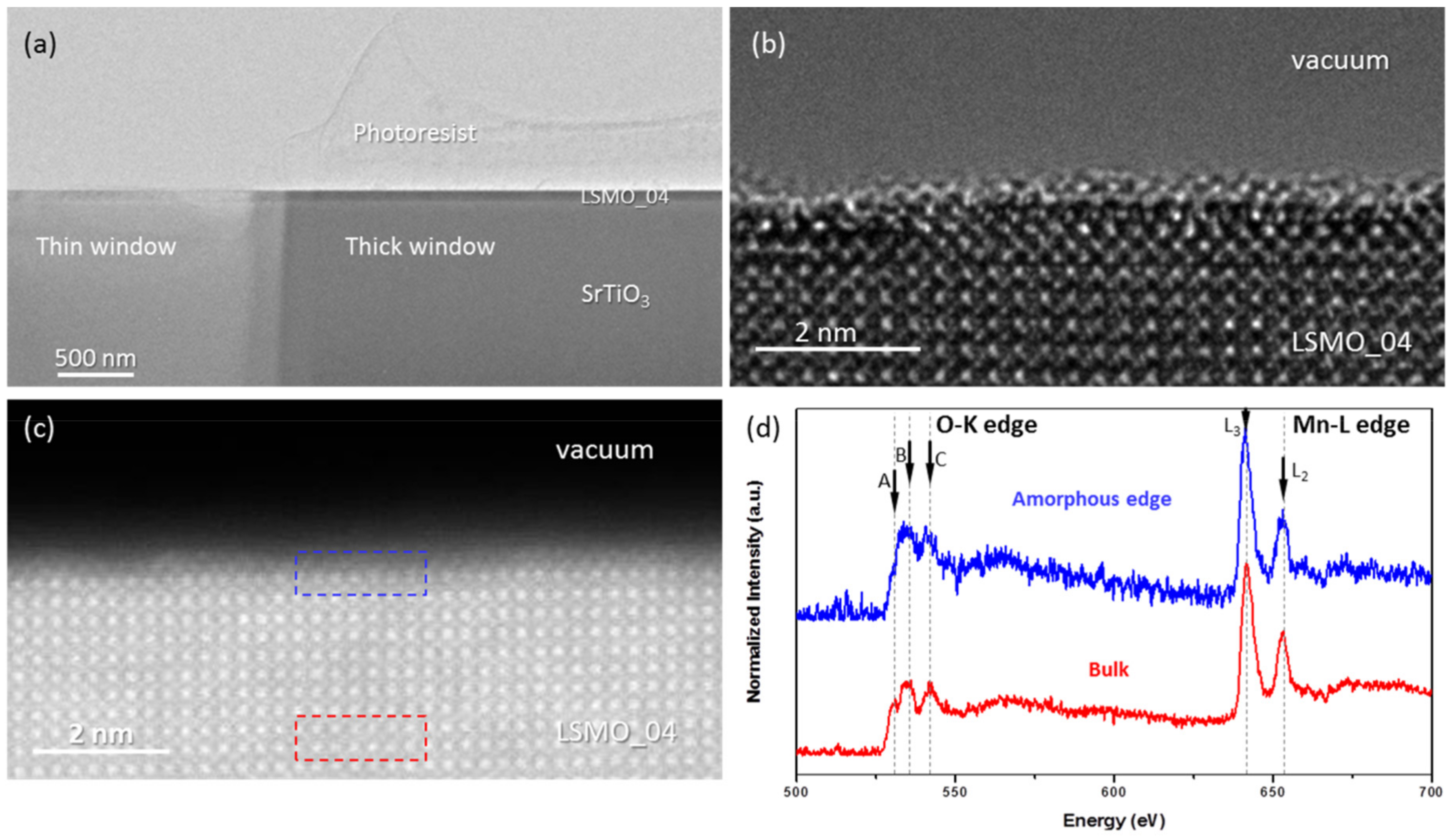
The low magnification cross-section image of LSMO (x = 0.4) specimen prepared using photoresist protection layer is shown in
Figure 1a. Two windows of different thickness are used to demonstrate the opportunity to control the thickness of lamella. The HRTEM image in
Figure 1b and HRSTEM image in
Figure 1c show that plasma cleaning during 5 min removes the rest of the photoresist completely.
Both the HRTEM and HRTEM images show that the ~40-50 nm thin lamella has a crystalline structure, despite a thin subunit-cell thick disordered surface layer. EELS spectra presented in
Figure 1d show that this disordered surface of LSMO film has lower oxidation state of Mn than the bulk. Three characteristic peaks of O K-edge are visible at 529 eV (A), 534 eV (B) and 543 eV (C). The prepeak (A) due to O 1s transitions to O 2p states hybridized with Mn 3d. It reflects the presence of O 2p holes. The other two peaks are due to transition from O 1s into O states which are hybridized with Ca d / Pr d states (B) and free electron like features (C) [
29]. Since oxygen vacancies are electron donors, a decrease in the intensity of the prepeak A indicates an increasing amount of oxygen vacancies. Its lack in the spectrum from the surface points to a reduced state of Mn. This is also confirmed by the analysis of the Mn L-edge. The Mn L edge is due to transition of the spin-orbit split 2p into Mn 3d states and thus shows L
3 and L
2 subfeatures. The L
3/L
2 intensity ratio is a measure of the Mn oxidation state [
30]. Our analysis yields an oxidation state between +2.6 and +2.8 for the amorphous material. Atomic force microscopy images of the same LSMO 0.4 films show crystalline surface which consist of atomically flat terraces and unit cell height steps [
28] as a result of step flow growth mode on vicinal SrTiO
3 (STO) (001). There is some evidence that crystalline LSMO films on SrTiO
3 can have reduced surfaces after vacuum annealing [
31]. Since the LSMO films studied here are annealed in oxygen after growth, complete oxidation of the surface as seen in [
31] is expected. We thus attribute surface disorder and Mn reduction of the TEM lamella shown in
Figure 1 to preparation-induced damage. Indeed, scattering of Ga ions during FIB thinning can give rise to preferential knock out of oxygen at the LSMO-photoresist interface.
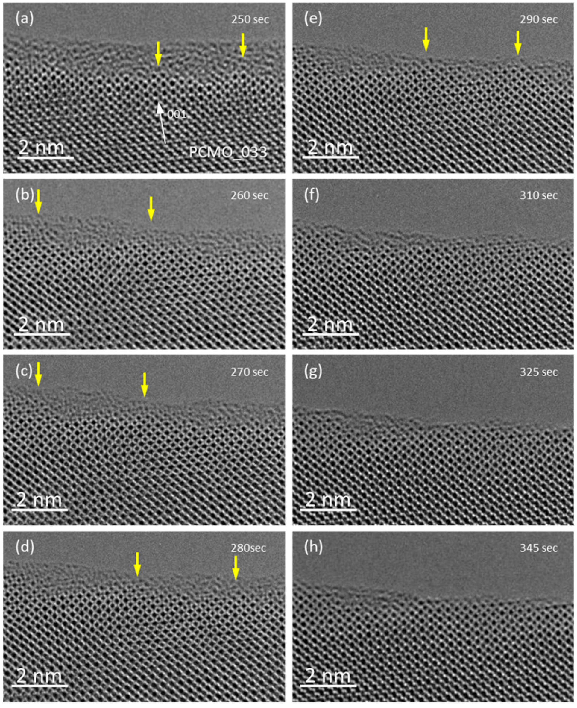
The possibility of a beam stimulated transformation of preparation induced surface disorder to the perovskite crystal structure is demonstrated for a 2–3 nm thick amorphous PCMO layer on top of crystalline PCMO x = 0.33 in different gases, i.e. He, N
2, and O
2 in
Figure 2. The cross-section lamellas have been cut from the PCMO/LSMO/Nb-STO stack; 300 kV electron beam stimulation is performed in TEM mode with a beam of about 100 nm in diameter and ~4 nA current. Such illumination conditions result in a 14,000–20,000 e
−·s
−1·Å
−2 dose rate. The process takes about 20–25 min in order to complete the transformation of the amorphous layers in He (
Figure 2a) or in N
2 (
Figure 2c) to a surface facets having of a length of about a few dozen nanometers,
Figure 2b,d, respectively. It is noteworthy that the first facets of several nanometers in length were formed already after the first three minutes. The corresponding movies S1, S2 and S3 show the real time changes of structure in N
2 gas (p
N2 = 5 ubar) at the beginning, after about 20 min and at the end of process, respectively. During all stages of process a pronounced atomic dynamics at the surface is observed similar to Epicier et al. [
32]. Also,
Figure 2b,d demonstrate that electron beam irradiation can result in different surface terminations. This will be discussed in detail further down. Thus, the process resembles the so-called solid phase epitaxial (SPE) growth, where an initially amorphous Si [
33] or complex oxide [
34] thin film is epitaxially recrystallized on a crystalline template at elevated temperatures. Remarkably, the electron-beam-induced SPE process in our environmental TEM study is observed at room temperature and depends on a reactive gas environment. The required electron flux is orders of magnitude lower than that reported for the transformation of amorphous STO into perovskite structure during operation the microscope in STEM mode (electron dose rate ≈ 1 × 10
8 e
−·s
−1·Å
−2, high vacuum conditions p = 10
−7 mbar) [
24].
The crystallization in O
2 gas proceeds similarly as in He or N
2, however, it takes only about 5–6 min at the same illumination conditions. Snapshots of crystallization in O
2 are presented in
Figure 3. At the beginning, during several minutes, only mobility of atoms in amorphous layer is visible, similar to observations in He or N
2 (
Figure 3a–d). Then, the growth of small pyramidal islands is observed (one island is marked with the yellow arrow). These islands grow slowly and over time reach the surface of amorphous layer (
Figure 3e). At the same time the thickness of amorphous layer is decreasing. Finally, the amorphous material between crystalline islands also becomes crystalline, and flat facets up to 10 nm in length are formed (
Figure 3f–h). It is important to note that in all gases (He, N
2 and O
2), the final phase of crystallization, i.e. when crystalline islands have sprouted through the amorphous layer, proceeds faster.
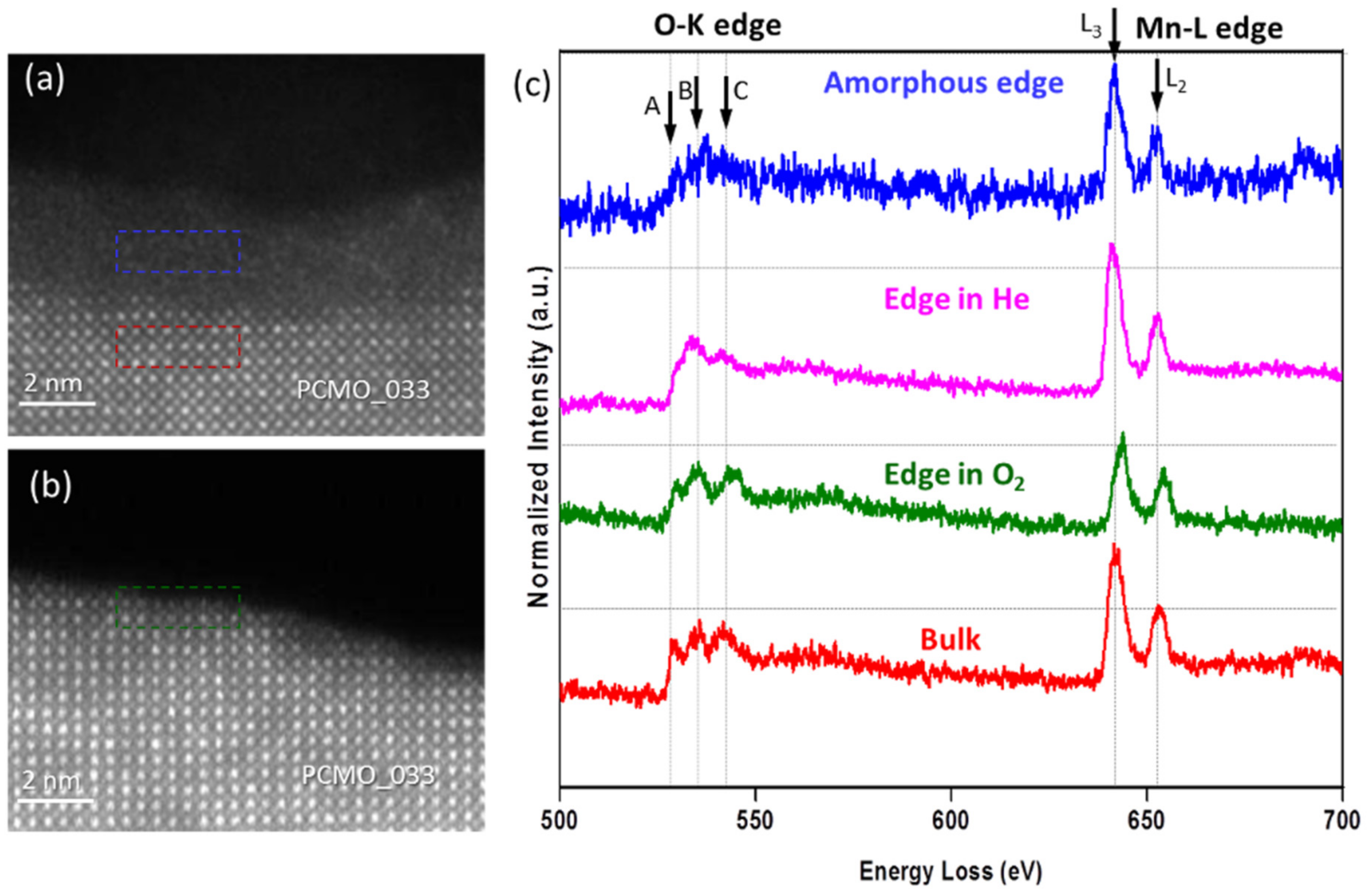
In order to verify the chemical composition of original, amorphous and recrystallized PCMO, the EELS spectra were collected at the beginning of experiment and after the recrystallization was completed. In addition, K- edges of oxygen and L-edges of Mn were collected with the better energy resolution to examine the oxidation state of Mn.
The HRSTEM images shown in
Figure 4a,b demonstrate an edge of PCMO (x = 0.33) film before and after recrystallization in oxygen at p
O2 = 50 ubar, respectively. Clean and atomically sharp steps having a height of few unit cells are commonly observed. The corresponding EELS spectra are shown in
Figure 4c. All spectra were aligned using a zero-loss peak (ZLP) as a reference, and then normalized. Note, that the spectrum collected from the amorphous edge looks noisier than other spectra because of smaller thickness of the edge. Based on the reduced intensity of the O K prepeak (A), the crystallization in He results in a reduced state of Mn at the surface. The analysis of L
3/L
2 ratio of Mn L-edge yields an average value of 3.30 ± 0.06 and a value of 3.24 ± 0.02 close to the surface (see
Figure S1). In contrast, when the crystallization was performed in O
2 the average value of the Mn oxidation state is 3.36 ± 0.06 and 3.35 ± 0.06 at the surface (see
Figure S2). All values are close to the value for the nominal composition as in bulk (+3.33). Thus, the use of oxygen leads to the epitaxial recrystallization of a stoichiometric PCMO, whereas in He, a crystalline edge with increased lattice disorder is developed. The average Mn valence state is the same in He as in O
2 within error based on the analysis of the L
3/L
2 intensity ratio. However, there is a strong reduction of the O K prepeak at the surface, pointing towards a more reduced state in He. The effect of disorder on electronic properties is quite complex. For example, in addition to oxygen vacancies, charge neutral pair defects can contribute to the lattice disorder in He which can maintain the Mn valence while changing the O K edge. Nevertheless, for all three gases used, the lattice spacing up to most top unit cell corresponds to the bulk PCMO material within error.
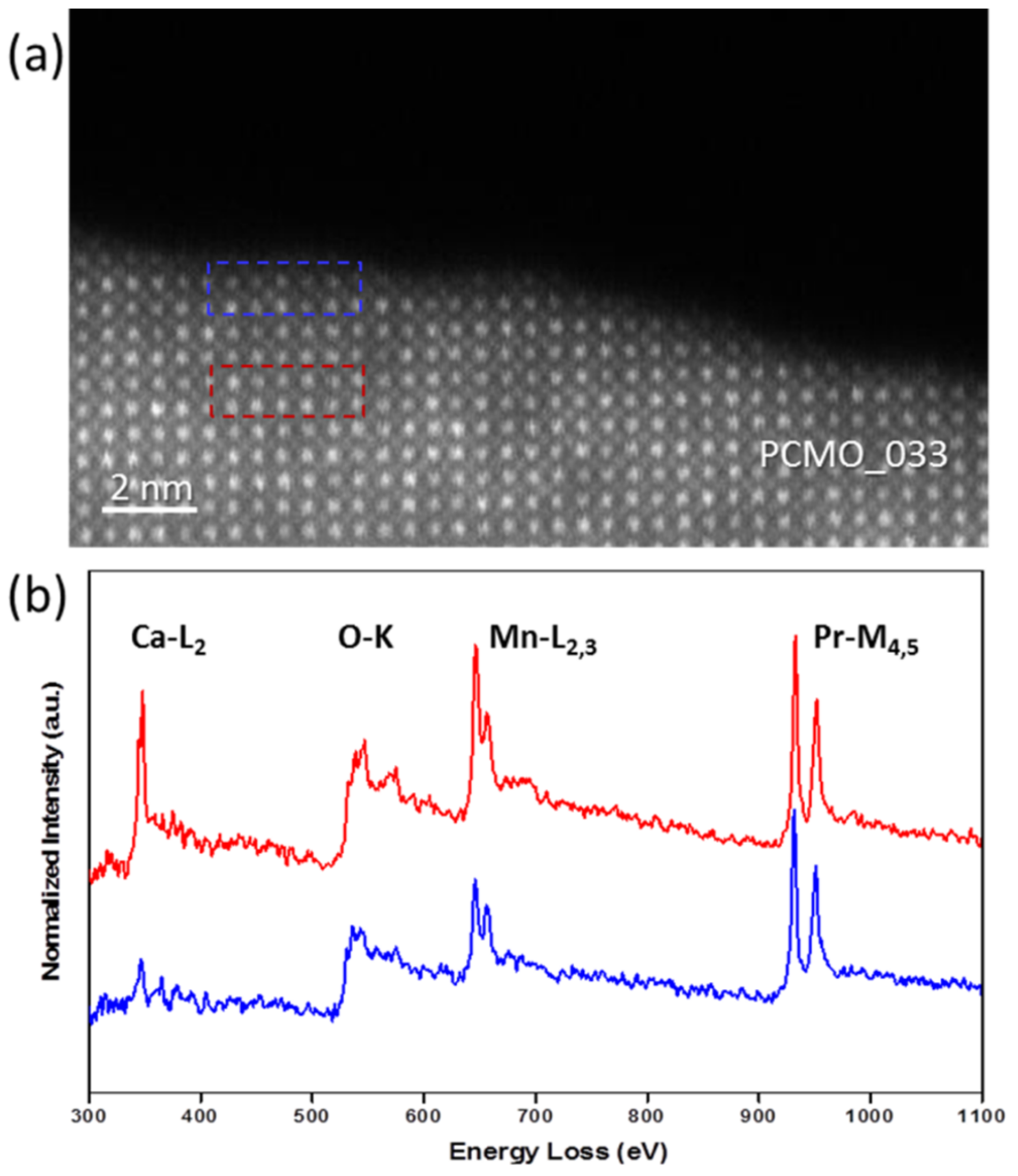
The chemical composition of the amorphous layer as well as recrystallized material was also verified using EELS, and only Pr, Ca, Mn, and O edges were detected;
Figure 5 shows the results for the PCMO, x = 0.33. A HRSTEM image of the recrystallized area is shown in
Figure 5a. The EELS spectra reveal a decrease of Ca content in the surface unit cells (
Figure 5b). Since the properties of perovskite materials strongly depend on the amount of doping, a careful choice of the illumination conditions and the environment is very essential for control of the chemical composition of the recrystallized perovskite. A long lasting electron beam illumination to fully recrystallize the amorphous layer obviously results in element-specific knock out damage of light elements which is evidenced by chemical analysis (
Figure 5). In addition, the lattice disorder of the recrystallized perovskite due to off-stoichiometry is visible by broadening of spots and changing of their intensities in corresponding FFT images calculated from the HRTEM images collected in all the gases used. The effect is notably less pronounced in series of HRTEM images collected from the same TEM lamella in O
2 (see
Figures S3 and S4), supporting our statement of a less vacancy disordered structure because Mn acquires its nominal valence state.
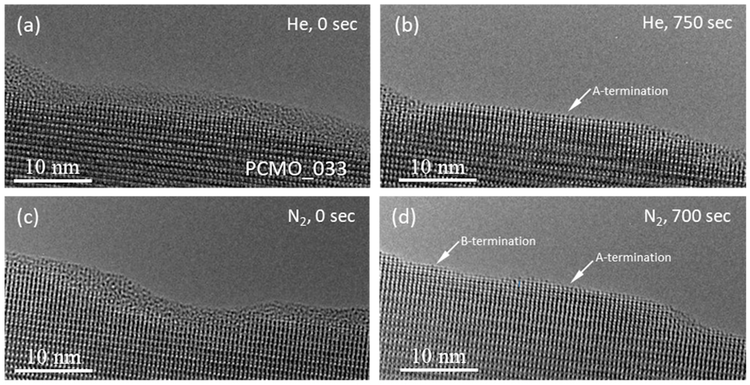
As it was already described above, that flat facets were formed from the amorphous material at the surface of PCMO in all He, N
2 and O
2 gases used. Moreover, a careful inspection of the top atomic layer revealed that the termination of the recrystallized edge depends on the gas used. This effect is shown in
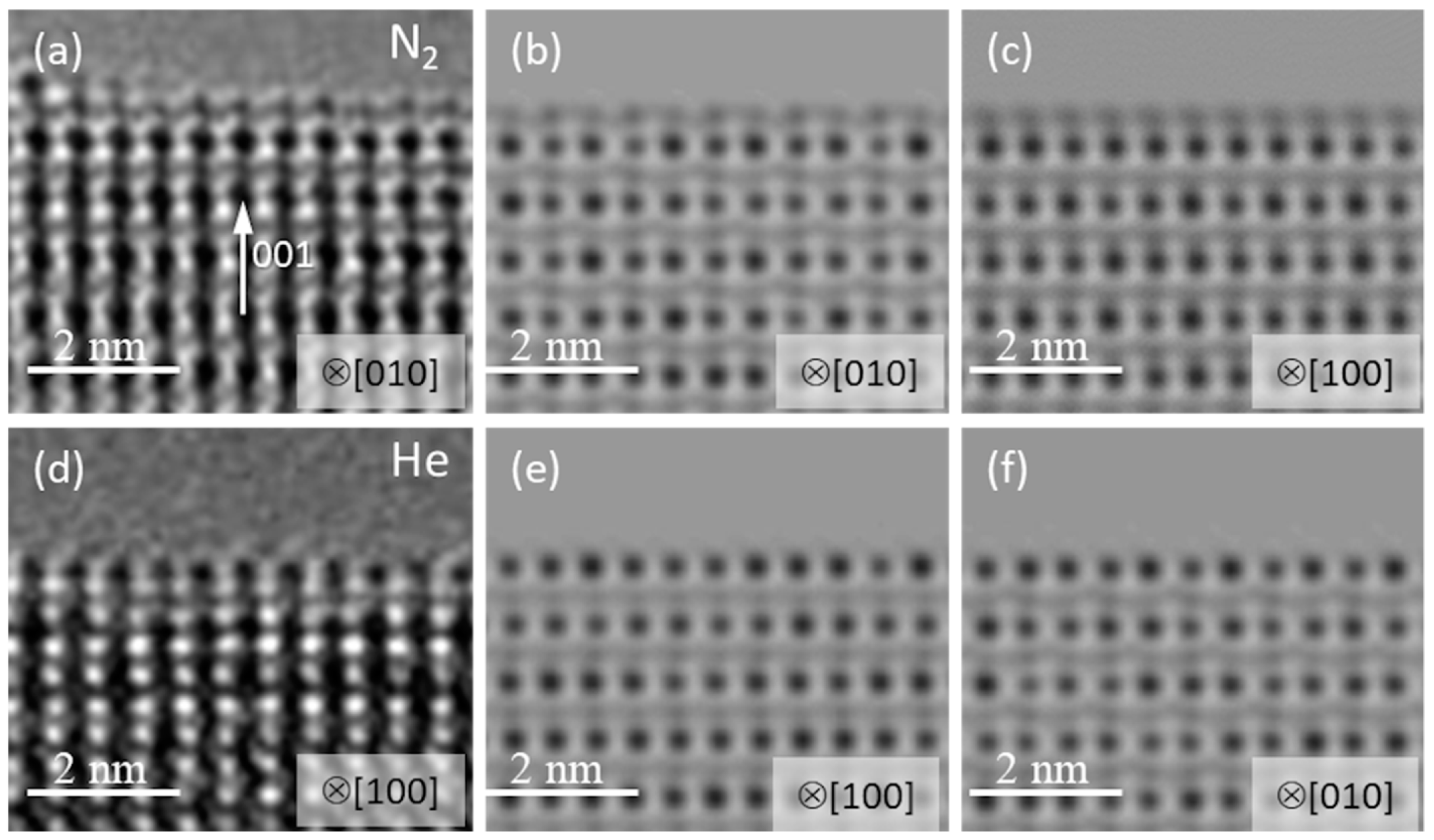
Figure 6. Both A- and B-cation stable terminations were observed after recrystallization in N
2 (
Figure 6a), while only the A-cation termination of facets was found after recrystallization in He (
Figure 6d). The observation is verified by HRTEM image simulations presented in
Figure 6b,c,e,f, respectively. The HRTEM images of PCMO along [100] and [010] look differently because of the symmetry inherent in the Pbnm space group. The Mn-O (B-termination along [010]) is obviously recognized in
Figure 6a,b because of a characteristic zigzag motif of Mn-O atomic columns (see
Figure S6 for details). In the case of A-termination the difference in HRTEM images along [100] and [010] is almost invisible.
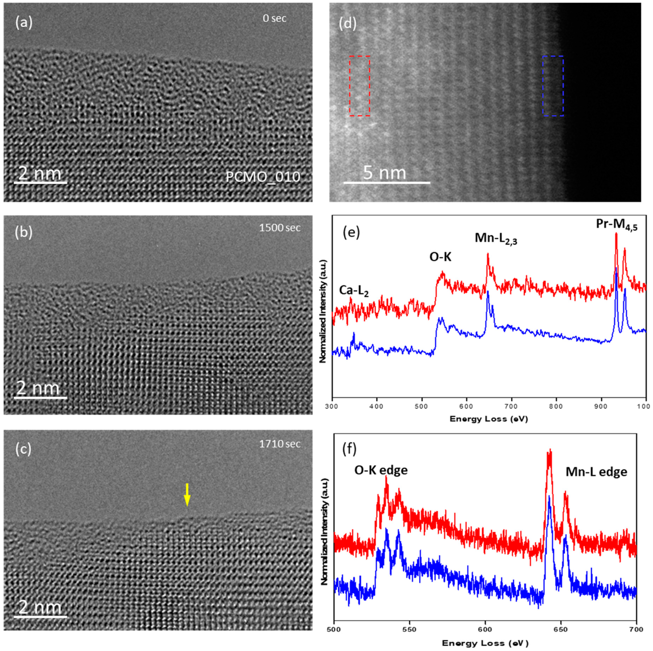
As an example for the recrystallization of PCMO (x = 0.1),
Figure 7a–c shows the evolution in He. The first crystalline facets showed up only after 28 min, compared with about 11 min for PCMO (x = 0.33). After such a long irradiation time, one can expect a high density of defects in the material. Indeed, the spots in the FFT image became more smeared after 28 min, which is evidence of the increased structural disorder (see
Figure S5). The weak signal of Ca is still visible in the EELS spectra taken from the edge (
Figure 7d,e) taking into account that the concentration of Ca is already very low in the original material. In general, the EELS data from PCMO (x = 0.1) sample are very scattered. In some areas the analysis of O-K and Mn-L edges shows that the oxidation state of Mn is in the +3.0–+3.3 range (
Figure 7f) pointing against a large concentration of single oxygen vacancies as origin of the lattice disorder. However, very low values of the oxidation state of Mn were also observed (
Figure S7).
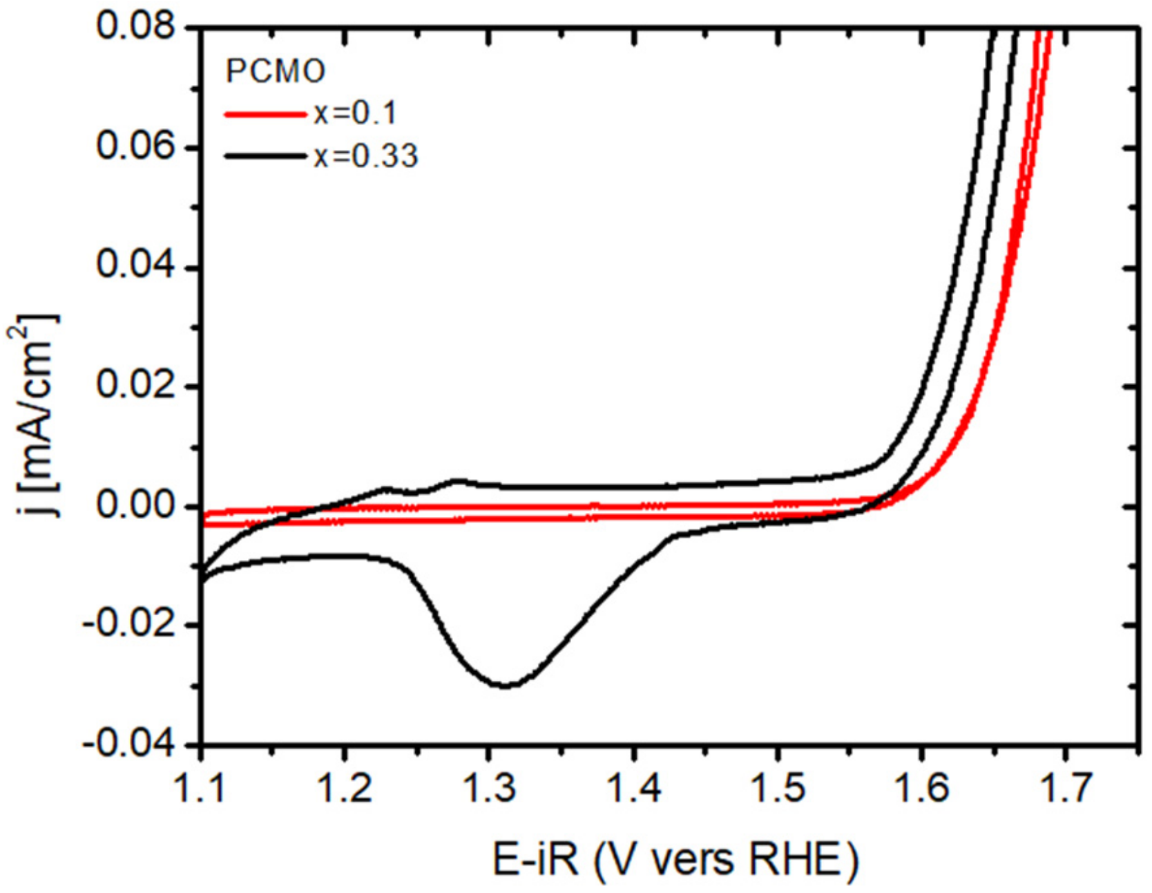
Usually, the recrystallization of the edge in PCMO (x = 0.1) took much longer for all gases used. This is however consistent with cyclovoltammetry studies, showing a pronounced surface Mn
2+/½V
O ↔ Mn
3+/O
O redox couple for PCMO (0.33) which is absent in x = 0.1. As an example,
Figure 8 shows cyclovoltagrams of two epitaxial (001) oriented PCMO (x = 0.1 and x = 0.33) films on LSMO/Nb:STO at pH = 13 measured at a sweep rate of 10 mV/s. The electrochemical measurements were performed in 0.1 M potassium hydroxide (KOH) electrolyte prepared by diluting KOH stock solution with deionized water (for neutral pH see [
17]). Both films show an exponential increase of currents at positive potential due to oxygen evolution reaction (OER), as verified by measuring the formed O
2 by a ring electrode. The pronounced redox peak for x = 0.33 indicates an easier oxygen vacancy formation and healing process compared to x = 0.1 which explains the observation of faster epitaxial recrystallization for x = 0.33 compared to x = 0.1 in the ETEM experiments.
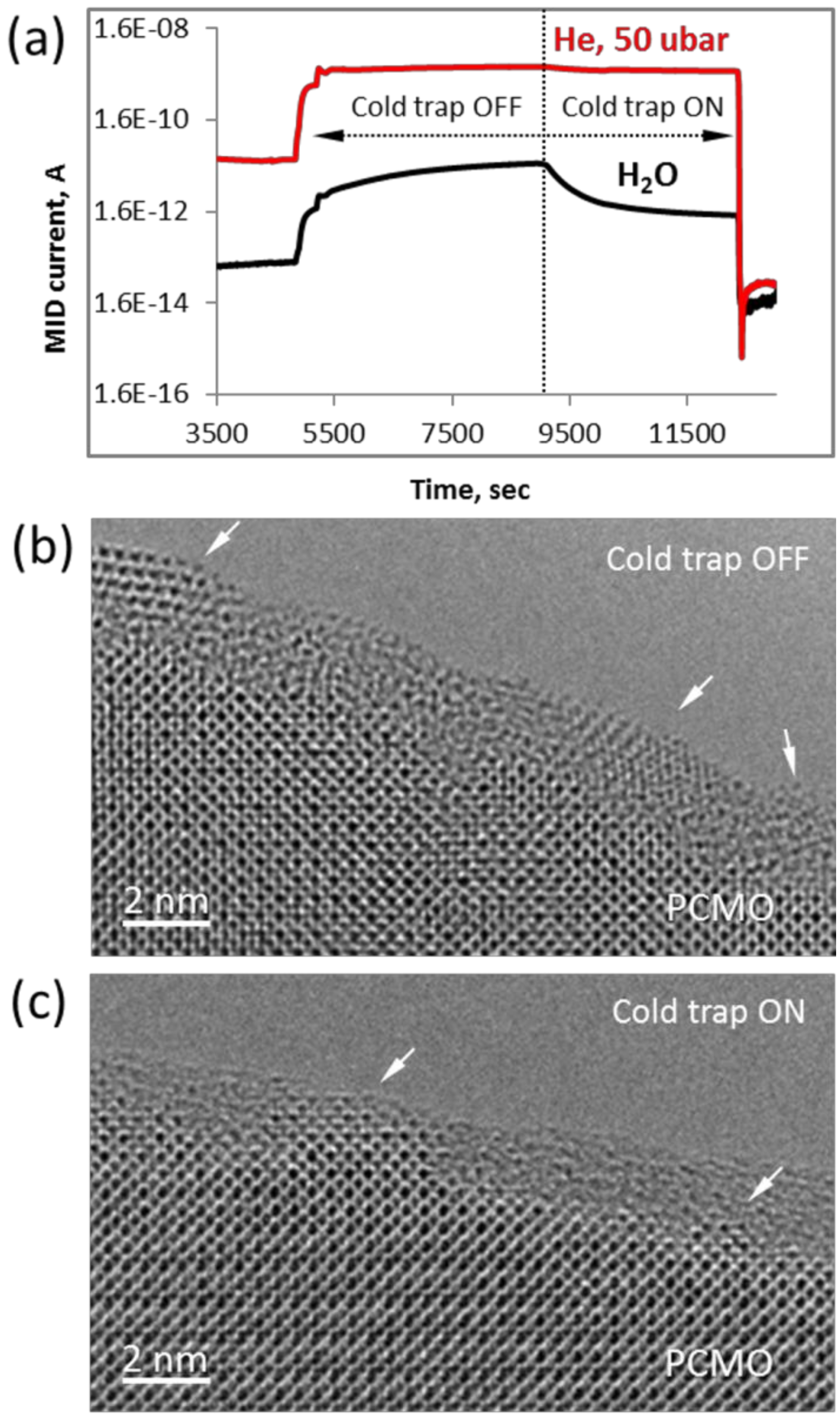
Finally, we note that the epitaxial crystallization only happens at the preexisting crystalline interface, when the partial water pressure is p
H2O < 5·10
−8 bar (
Figure 9). In other words, the residual pressure of water vapor in the column should be below 0.1% of the working gas. Exemplary snap shot from the Quadera™ software (
Figure 9a) shows two periods during the experiment in He when the cold trap was not used (Cold trap OFF) and after it was activated (Cold trap ON). At the higher pressure of water vapor (p
H2O = 25·10
−8 bar, Cold Trap OFF) the amorphous layer was transformed into randomly oriented PrO
2 particles as shown in
Figure 9b (see also
Figure S8). Similar structural transformations of initially amorphous areas were reported earlier for the ETEM experiments performed in water vapor at higher pressures of 5·10
−6 and 5·10
−5 bar [
18], and this is consistent with the drop of OER activity in electrochemical experiments over time due to Mn leaching into the electrolyte [
28]. After the cold trap was filled with liquid nitrogen and as soon as the partial pressure of water vapor dropped about an order of magnitude (p
H2O = 25·10
−9 bar), the epitaxial recrystallization was observed (
Figure 9c) similar to results presented in
Figure 2,
Figure 3 and
Figure 4.
3. Discussion
As already mentioned, the observed recrystallization of amorphous PCMO resembles SPE of an amorphous Si which happens via a moving amorphous/crystalline interface, where velocities of a few nm per min requires elevated temperatures above 500 °C [
33]. The recrystallization temperature can be significantly reduced to around 200–300 °C, if the recrystallization is assisted by ion irradiation [
34]. Although the electron-beam induced recrystallization reported here also happens via the movement of the crystalline/amorphous interface, it however strongly differs from the SPE. First of all, the beam induced temperature increase ΔT in the TEM lamella is irrelevant, excluding a thermally activated growth mechanisms. The upper limit of temperature increase for the used beam parameters is Δ T = 0.015 K (see
Appendix A). Furthermore, the epitaxial recrystallization in our experiments strongly depends on the gas environment. In high vacuum conditions, no epitaxial growth is observed. Here, the amorphous layer partially disappears on timescales of tens of minutes due to electron beam-induced sputtering of atoms from damaged areas.
In oxygen both amorphous PCMO x = 0.1 and x = 0.33 layers transform into a crystalline perovskite layer under oxygen uptake during the recrystallization process. This is confirmed by a change of the Mn valence state from about +2.9 in the amorphous to close to the nominal value. There are three possible candidates for beam induced electronic excitations driven the observed solid state chemistry: (i) a photo-chemical process driven by beam induced generation of hole carriers. Since the lifetime of photo-holes (1 ns) is orders of magnitudes below the recrystallization rate (1 s per atom), a photo-chemical process is highly improbable. (ii) An electrochemical process driven by beam induced positive electric potentials due to secondary electron emission. Such an electrochemical mechanism is feasible: The relevant redox potential for oxygen in manganites is of the order of 1 V (see
Figure 8), a potential which can be easily generated in semiconductors at dose rates above 10.000 e/Å
2s [
35]. (iii) Radiolysis, the dissociation of molecules or covalently bound solids by inelastic scattering of primary electrons with bond forming valence electrons. Whereas radiolysis may be relevant for the dissociation of molecular oxygen and activation of O
2 for the solid state reaction, it is irrelevant in ionic or metallic solids. Here, this is confirmed by the formation of rather perfect crystalline perovskite structure in O
2.
Beam-induced displacements of atoms by nuclear collisions is probable process for activating the growth of crystalline PCMO by a moving amorphous/crystalline interface as observed in O2 as well as in the inert gases N2 and He. However, it cannot explain the oxygen uptake in O2. Maximum energy transfer takes place by backscattering of electron which could displace surface adsorbed oxygen into the amorphous material on the top side of the lamella, but would lead to sputtering on the bottom side and at the edge. This would represent an “inverse sputtering process”, where in contrast to HV, oxygen vacancies are filled by activated surface oxygen. Conversely, in N2, one should then form oxynitrates, in contrast to observation.
The observation that the amorphous phase transforms into crystalline PrO
x nanoparticles in the presence of sufficient partial pressure of H
2O by preferential leaching of Mn and also Ca give strong hints about the beam induced chemistry involved. Based on the equation provided by Egerton et al. [
36], for the energy transfer between a high energy electron and an atom due to elastic scattering, we calculate the upper limit for the different atomic species:
Emax is 53.1 eV (O
2), 42.5 eV (Ca), 34.0 eV (Mn) and 14.4 eV (Pr). This must be compared to binding energies of
Eb = 50 eV (O), 70 eV (A site) [
14] and between 50–170 eV (Ti as an exemplary B-site in BaTiO
3) [
37], depending on the crystal orientation of a perfect perovskite single crystal. This is consistent to the statement that
Emax < Eb. However,
Eb should be generally reduced in the amorphous phase of the same chemical elements, because of the lower density of packing, open voids and change of bond coordination. Remarkably, our experiments show that the preferential sputtering of atomic species strongly depends on the gas environment. In HV, the amorphous surface layer is partially removed with preferential sputtering of O, Ca and Mn without formation of PrO
x. In contrast, in O
2 or inert gases, the presence/absence of preferential leaching of Mn and Ca strongly depends on the p
H2O. This reflects that the vacancy formation energy close to surfaces depends on the surface chemistry. The presence of adsorbed surface H
2O, where Mn
2+ and Ca
2+ is soluble, clearly facilitates the leaching of displaced Mn and Ca species, giving rise to the formation of PrO
x. In contrast, in O
2 this process is suppressed and the uptake of oxygen for example by occupation of V
O vacancy sites is the dominating process.
Clearly, the crystallization rate and thus the velocity of the amorphous/crystalline interface is slowed down in inert gases He and N
2, compared to experiments in O
2. This indicates, that beam induced atomic displacements cannot be the only driving force for the movement of the interface.
Figure S9 shows that residual molecular and atomic oxygen is also present in an inert gas experiment, e.g., in He. Its relative concentration is only slightly reduced after switching on the cold trap. The epitaxial recrystallization in inert gases may thus be influenced by the presence of oxygen. The analysis of the Mn valence state after He in comparison with the amorphous material at the pristine lamellas does not provide evidence for a large amount of oxygen uptake, since the Mn valence state is the same within error. However, sputtering of oxygen may be still compensated by the electrochemical oxidation, which is slowed down at lower p
O2. This could indicate that beam induced epitaxial recrystallization in inert gases is also accompanied by a solid state chemical reaction with oxygen. Consequently, even without net uptake of oxygen, the presence of surface adsorbed oxygen species can alter the beam induced effects from absent in high vacuum, over leaching in H
2O to perovskite epitaxy in inert gases.
4. Materials and Methods
Thin films of Pr
1-xCa
xMnO
3 (PCMO) with different Pr/Ca ratio (x = 0.1 and x = 0.33) were grown on Nb-doped SrTiO
3 (001) with a 20 nm thick epitaxial La
0.6Sr
0.4MnO
3 (LSMO) (001) interlayer by reactive Xe-ion beam sputtering in an oxygen atmosphere with a partial pressure of 1.4·10
−4 mbar at the deposition temperature of T
dep = 1020 K. The PCMO film of thickness of d ≈ 100 nm reveals epitaxial growth with [001]/[110] growth domains, inevitably present due to twinning. The LSMO interlayer was grown in order to adjust the lattice misfit between STO and PCMO. The growth parameters and detailed structural characterization of studied films is published elsewhere [
17,
18,
28].
Specimens for in situ TEM studies were prepared by lift-out technique using a NanoLab 600 (Thermo Scientific™, former FEI, Hillsboro, Oregon, USA) dual beam instrument operated at 30 and 5 kV. Conventional method with FIB lift-out technique usually starts from the deposition of platinum/carbon (Pt/C) protection layers by electron or ion beam [
38]. Since Pt is highly active catalyst, its presence at the surface of perovskites should be excluded. All lamellas in this study were prepared using a protection layer of Alkali Resistant Positive Photoresist X AR-P 5900/4 (ALLRESIST GmbH, Strausberg, Germany) which was deposited onto the surface of LSMO and PCMO thin films before FIB cutting procedure. Electron transparent lamella was finally cleaned with Ar
+ ions with energies from 500 eV to 100 eV using a Gatan PIPS 691 ion polishing system. The rest of protection layer was removed with a plasma cleaner prior TEM studies. High-resolution TEM (HRTEM), electron diffraction (ED) and STEM studies were performed using an aberration corrected Titan 80-300 environmental microscope (Thermo Scientific™, former FEI, Hillsboro, Oregon, USA) operated at 300 kV. The specimens were imaged along [010] and [110] crystallographic directions in the Pbnm space group. ETEM experiments are performed with N
2, He, O
2 gases. The chemical composition of gas environment was controlled by the Residual Gas Analyzer (RGA) QMG220 (Pfeiffer Vacuum GmbH, Germany) controlled by Quadera™ software (version 4.3, INFICON Aktiengesellschaft, Liechtenstein, 2010). During the experiments the deviations of pressure from desired values of 5 and 50 microbars did not exceed 5%. Other residual gases are always present in the inlet tubes and electron microscope column. In order to minimize their influence the inlet tubes were purged firstly with the working gas. Then, the specimen chamber was also purged with the working gas during at least half an hour, and the electron beam was blanked. These procedures allowed reducing the presence of other gases to be less than 1%. For example, during the used experimental setting, typical values are H
2O: 1% (cold trap off) and 0.05% (cold trap on); O
2: 0.2%; N
2: 0.04%; hydrocarbons (unspecified) and very low amounts of atomic nitrogen and oxygen. Switching on the cold trap thus changes the main residual gas impurity from H
2O to O
2 (see SI1). EELS data were collected with a Gatan Imaging Filter (GIF) Quantum 965ER (Gatan, Pleasanton, CA, USA). Atomic models were built using the Vesta software package (version 3.4.7, 2019) [
39]. High-angle annular dark field (HAADF) contrast and spectrum imaging was used in order to visualize change in chemical composition. HRTEM images were simulated using QSTEM software (version 2.51, 2019) [
40].

