The Formation Mechanism and Model of the Surface Nanoscale Kirkendall Effect on Au Catalyst Island/GaAs Substrate by Thermal Vapor-Liquid-Solid Method with Two-Step Temperature Mode


Abstract
1. Introduction
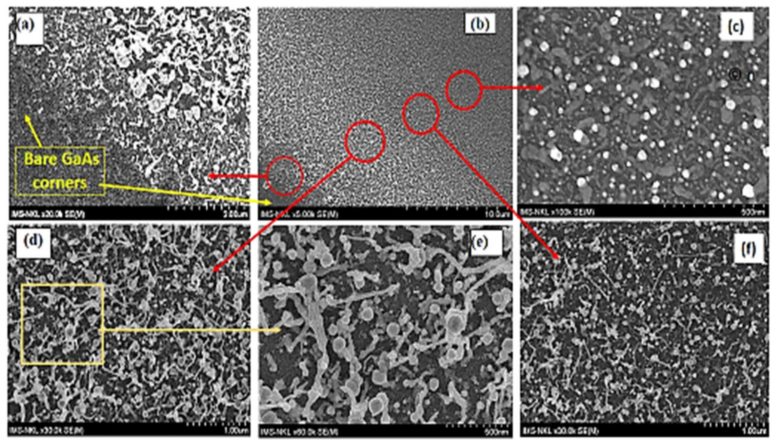
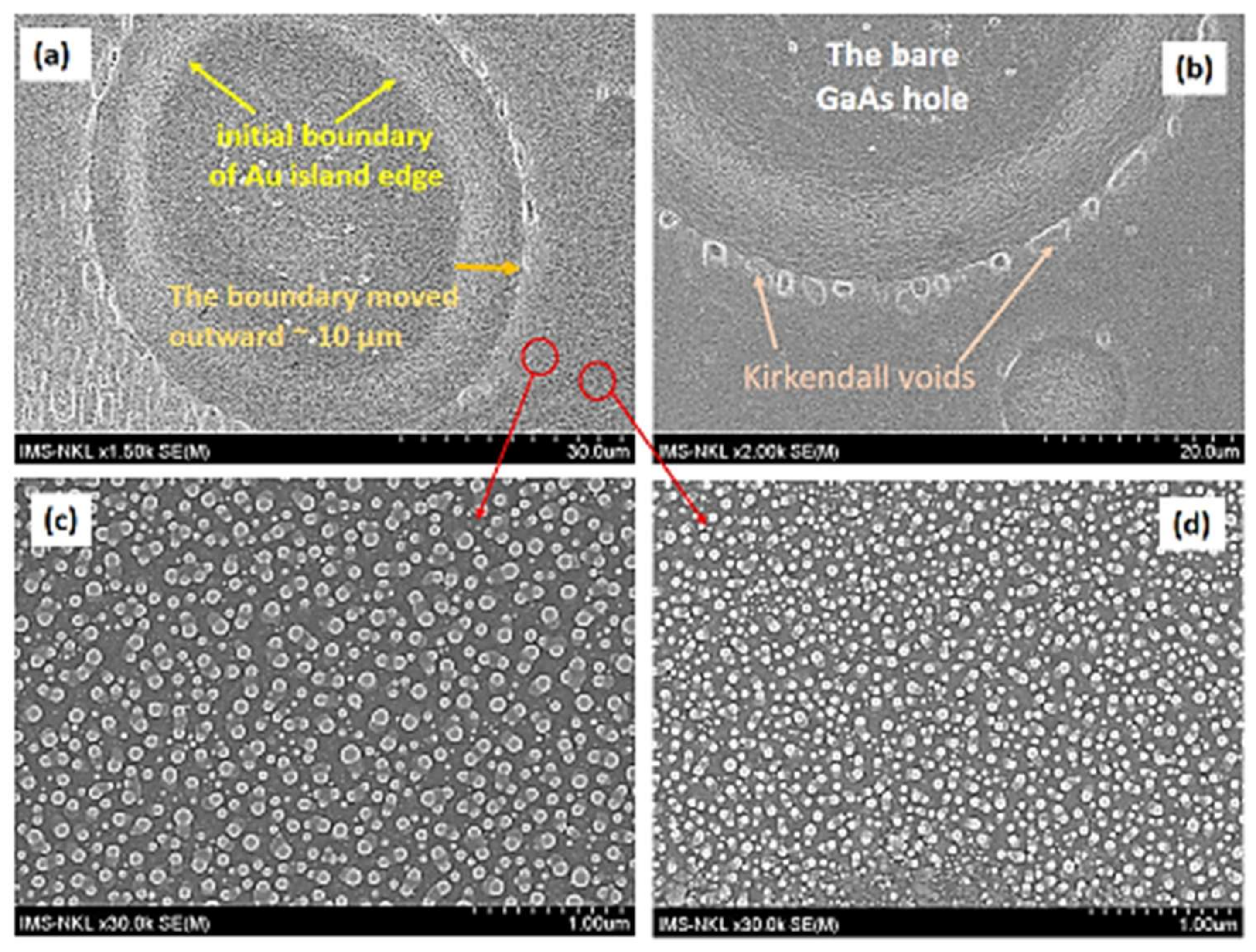
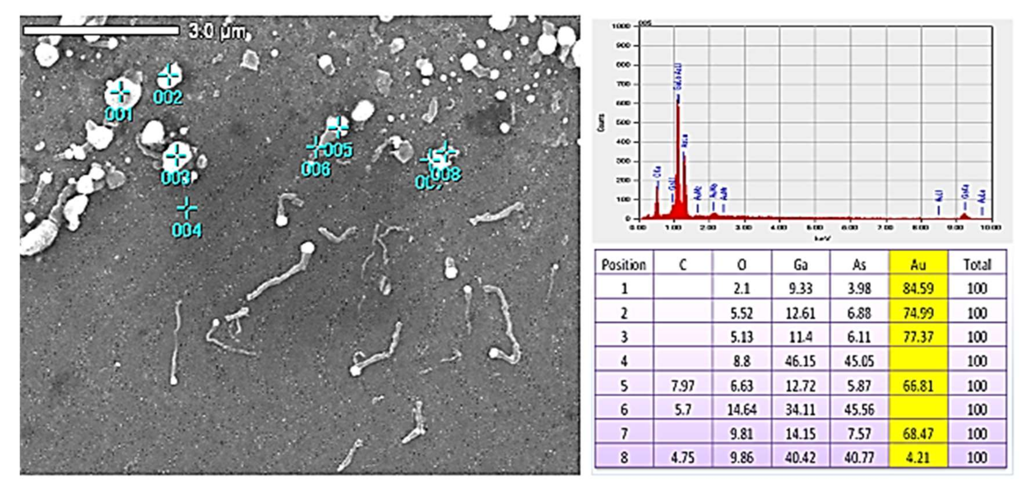
2. The Experimental Results
3. Discussion
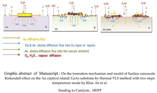
3.1. On the Formation Mechanism of SNKE
- -
- on the surface of the conventional bulk material (so-called SKE)
- -
- on the surface of nanoscale subjects (or on the interface between two nanoscale subjects in the defined bulk material environment (so-called NSKE)
- -
- on the surface of a mixed system including the surface of nanoscale subjects and on the bulk material (substrate) surface, as in our case (so-called SNKE).
3.2. The Role of Au Metal Catalyst Amount in the Phase Transfer Catalysis and Kinetics of Reactions for the Formation of SNKE
3.3. Numerical Estimation of SNC Diffusivity
3.4. On the Formation of the Nano Material Configurations Outside the Au Catalyst Island
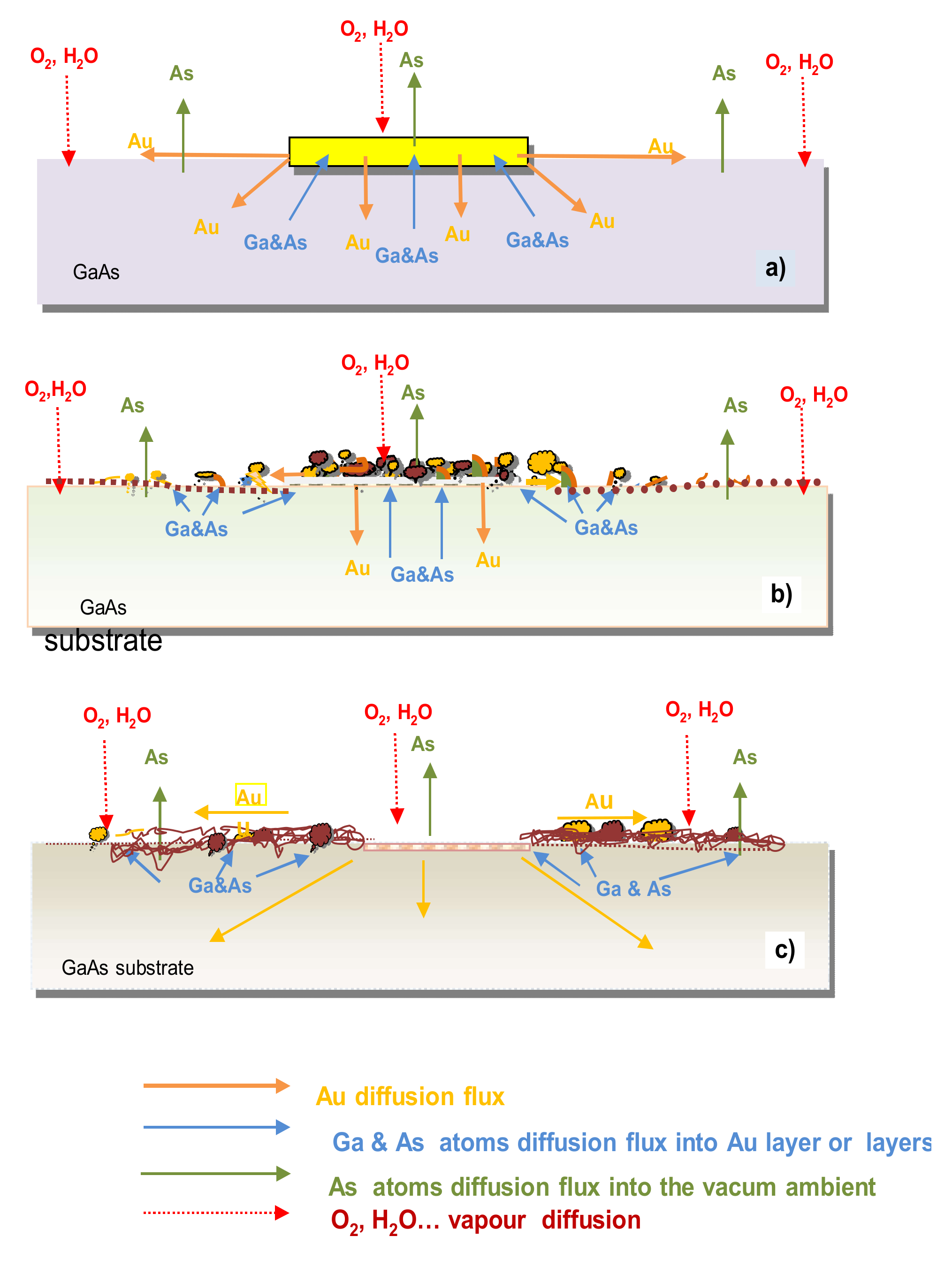
3.5. The Proposed Model of SNKE Formation
3.6. The Advantages and Disadvantages of SNKE and Applications
- (a)
- The advantages of SNKE
- -
- The SNKE can be clearly observed directly on the semiconductor substrate surface; meanwhile, the NKE are formed in hollow nanotubes and hollow nanospheres, where their phenomena are hard to observe directly.
- -
- The SNKE can be controlled by changing the temperature profile and annealing–growing times, and especially by changing the thickness of the Au metal catalyst island (Au amount). We could control the degree of formation of SNKE with several options, as follows:
- We can grow the NWs normally with the traditional VLS method without SNKE if the thickness of the Au metal catalyst island is smaller than 20 nm.
- We can produce the SNKE with primarily growth of NPs only if we choose a moderately low Au island thickness in the range of 35 nm to 100 nm, a low T1 decomposition temperature (410 °C), a T2 (610–620 °C) temperature that is lower than the Eutectic temperature (630 °C).
- We can produce the SNKE with primarily growth of NWs if we choose a moderately low Au island thickness in the range of 35 nm to 100 nm, a low T1 decomposition temperature (410 °C) and a T2 (610–620 °C) temperature lower than the Eutectic temperature (630 °C).
- We can produce SNKE with the growth of mixed configurations of nanomaterials (NPs, NWs, NRs) if we choose a thick Au metal catalyst thickness (>200–1000 nm) and high temperature modes (T1 = 440 °C and, T2 = 640 °C).
- We can produce SNKE with the growth of NWs with strong or weak bases on the GaAs substrate if we choose a moderate T1 temperature (400–410 °C) and a T2 temperature higher than the Eutectic temperature (630 °C) with a long growing–diffusion time t4.
- (b)
- The disadvantages of SNKE
- -
- During the fabrication of a micro nano integrated circuit on the AIIIBV substrate material, the Au strips/islands are often evaporated (or sputtered) onto the semiconductor substrate surface; this is followed by a thermal annealing process in a moderately high temperature range from 200 to 400 °C in order to produce a metal contact system on the semiconductor surface. If we do not take care of the technological process, the disadvantages of SNKE could predominate: the outward diffusion to further distances from the Au islands and/or Au strips, which could cause short circuit faults in nano devices or in micro- and nanoscale integrated circuits. We think that a similar effect could also occur for strips/islands of other metals (Ni, Fe, Ag, Al, etc.) on semiconductors (Si, InSb, Ge, etc.) used as interconnection contacts.
- -
- The formation of SNKE could result in tissue loss due to uneven surfaces, local defects, and hole and pit etchings; these could generate several problems on semiconductor surfaces that contain micro and nano devices or integrated circuits, causing the loss in the form of current leakage and other effects.
4. Materials and Methods
5. Main Conclusions
Supplementary Materials
Author Contributions
Funding
Acknowledgments
Conflicts of Interest
References
- Kirkendall, E.; Thomassen, L.; Upthegrove, C. Rates of Diffusion of Copper and Zinc in Alpha Brass. Trans. AIME 1939, 133, 186–203. [Google Scholar]
- Kirkendall, E.O. Diffusion of Zinc in Alpha Brass. Trans. AIME 1942, 147, 104–110. [Google Scholar]
- Tu, K.N.; Gösele, U. Hollow nanostructures based on the Kirkendall effect: Design and stability considerations. Appl. Phys. Lett. 2005, 86, 093111. [Google Scholar] [CrossRef]
- Fan, H.J.; Gösele, U.; Zacharias, M. Formation of Nanotubes and Hollow Nanoparticles Based on Kirkendall and Diffusion Processes: A Review. Small 2007, 3, 1660–1671. [Google Scholar] [CrossRef]
- Prasad, S.; Paula, A. Theoretical consideration on the formation of nanotube following the Kirkendall effect. Appl. Phys. Lett. 2007, 90, 233114. [Google Scholar] [CrossRef]
- Wang, W.; Dahl, M.; Yin, Y. Hollow Nanocrystals through the Nanoscale Kirkendall Effect. Chem. Mater. 2013, 25, 1179–1189. [Google Scholar] [CrossRef]
- Wagner, R.S.; Ellis, W.C. Vapor-liquid-solid mechanism of single crystal growth. Appl. Phys. Lett. 1964, 4, 89. [Google Scholar] [CrossRef]
- An, D.K.; Chung, N.X.; Trang, P.H.; van Vuong, H.; Phong, P.V.; Tuan, P.A. On growth mechanisms and dynamic simulation of growth process based on the experimental results of nanowire growth by VLS method on semiconductor substrates. J. Phys. Conf. Ser. 2009, 187, 1. [Google Scholar] [CrossRef]
- Dao, K.A.; Phan, A.T.; Do, H.M.; Luu, T.H.; Falke, M.; MacKenzie, M. The influences of technological conditions and Au cluster islands on morphology of Ga2O3 nanowires grown by VLS method on GaAs substrate. J. Mater. Sci. Mater. Electron. 2011, 22, 204–216. [Google Scholar] [CrossRef]
- Yin, Y.; Rioux, R.M.; Erdonmez, C.K.; Hughes, S.; Somorjai, G.A.; Alivisatos, A.P. Formation of Hollow Nanocrystals Through the Nanoscale Kirkendall Effect. Science 2004, 304, 711–714. [Google Scholar] [CrossRef]
- El Mel, A.B.; Nakamura, R.; Bittencourt, C. The Kirkendall effect and nanoscience: Hollow nanospheres and nanotubes. Beilstein J. Nanotechnol. 2015, 6, 1348–1361. Available online: https://www.beilstein-journals.org/bjnano/articles/6/139 (accessed on 20 September 2019). [CrossRef] [PubMed]
- Mohammad, S.N. For nanowire growth, vapor-solid-solid (vapor-solid) mechanism is actually vapor-quasisolid-solid (vapor-quasiliquid-solid) mechanism. J. Chem. Phys. 2009, 131, 224702. [Google Scholar] [CrossRef] [PubMed]
- Zheng, Y.F.; Tang, Y.-H.; Wang, N.; Yu, D.P.; Lee, C.S.; Bello, I.; Lee, S.T. Silicon nanowires prepared by laser ablation at high temperature. Appl. Phys. Lett. 1998, 72, 1835. [Google Scholar] [CrossRef]
- Mohammad, N.S. Investigation of the oxide-assisted growth mechanism for nanowire growth and a model for this mechanism. J. Vac. Sci. Technol. B Microelectron. Nanom. Struct. 2008, 26, 1993–2007. [Google Scholar]
- Surface Diffusion—Wikipedia. Available online: http://en.wikipedia.org/wiki/surface_diffusion (accessed on 20 September 2019).
- Weizer, V.G.; Fatemi, N.S. The interaction of gold with gallium arsenide. J. Appl. Phys. 1988, 64, 4618. [Google Scholar] [CrossRef]
- Liliental-Weber, Z.; Washburn, J.; Newman, N.; Spicer, W.E.; Weber, E.R. Morphology of Au/GaAs interfaces. Appl. Phys. Lett. 1986, 49, 1514. [Google Scholar]
- Akiyama, O.T.; Haneda, Y.; Nakamura, K.; Ito, T. Role of Au/GaAs (111) interface on the wurtzite-structure formation during GaAs nanowire growth by vapor-liquid-solid mechanism. Phys. Rev. 2009, 79, 153406. [Google Scholar] [CrossRef]
- Yoshiie, T.; Bauer, C.L.; Milnes, A.G. Interfacial reactions between gold thin films and GaAs substrates. Thin Solid Films 1984, 111, 149–166. [Google Scholar] [CrossRef]
- Chen, B.; Fu, X.; Tang, J.; Lysevych, M.; Tan, H.H.; Jagadish, C.; Zewail, A.H. Dynamics and control of gold-ncapped gallium arsenide nanowires imaged by 4D electron microscopy. PNAS 2017, 114, 12876–12881. [Google Scholar] [CrossRef]
- Shaw, D. Atomic Diffusion in Semiconductors; Plenum: New York, NY, USA, 1973. [Google Scholar]
- Kang, Y.; Li, X.; Gong, H.; Jiang, R. Semicond. Sci. Technol. 2003, 18, 607–610. [Google Scholar]
- Fisher, D.J. Diffusion in GaAs and Other III-V Semiconductors; SCITEC Publications; Volume 157–159, Available online: http://www.pearton.mse.ufl.edu/semic properties/data/5032.pdf (accessed on 17 May 2019).
- Tan, T.Y. Point defects and diffusion mechanisms pertinent to the Ga sublattice of GaAs. Mater. Chem. Phys. 1995, 40, 245–252. [Google Scholar] [CrossRef]
- Luken, K.M.; Morrow, R.A. Diffusing arsenic vacancies and their interaction with the native defect EL2 in GaAs. J. Appl. Phys. 1996, 79, 1388–1390. [Google Scholar] [CrossRef]
- Swaminathan, V.; Caruso, R.; Pearton, S.J. Photoluminescence from annealed semi-insulating GaAs crystals: The 1.360-eV band. J. Appl. Phys. 1988, 63, 2164–2167. [Google Scholar] [CrossRef]
- Gösele, U.; Tan, T.Y.; Schultz, M.; Egger, U.; Werner, P.; Scholz, R.; Breitenstein, O. Diffusion in GaAs and Related Compouds: Recent developments. Defect Diffus. Forum 1997, 143–147, 1079–1094. [Google Scholar] [CrossRef]
- Seebauer, E.G.; Allen, C.E. Estimating surface diffusion coefficients. Prog. Surf. Sci. 1995, 49, 265–330. [Google Scholar] [CrossRef]
- Dao, K.A.; Nguyen, T.D.; Phan, A.T.; Do, H.M. On the formation of voids, etched holes, and GaO particles configuration during the nanowires growth by VLS method on GaAs substrate. J. Mater. Sci. Mater. Electron. 2013, 24, 2513–2520. [Google Scholar] [CrossRef]


| Name of Element Diffusion and/ or Surface Clusters | In Materials (Substrate, Samples, NW, Symbols…) | Diffusion Temperature (°C) | Name of Element Diffusivity | Published Data of Element Diffusivity (m2/s or cm2/s) | Reference (Calculated or Estimated Methods) |
|---|---|---|---|---|---|
| Ga diffusion | GaAs | 640 | Ga atom diffusivity | DGa(ni)=4 × 10⁻²⁵to 10−20 (cm2/sec) depending on vacancies, interstitials | [27] U.Gösele at al. |
| Ga diffusion | GaAs | 795 1230 | Ga atom diffusivity (DGa) | 6.9 × 10⁻¹⁹ cm2/s 3.3 × 10⁻¹³ cm2/s | [24] T.Y.Tan |
| Ga diffusion | 40 nm polycrystalline Gold | 540 | Ga atom diffusivity | 1.2 × 10⁻¹⁷ m2 s−1 | [23] Editor by D.J. Fisher |
| Au diffusion | In the growing GaAs nanowire | 725 K | Au diffusivity In NW grown from Au/GaAs | order of 10−4 cm2/s | [20] Bin Chen et. al. by random walk theory, D ~ L2/ τ |
| Au diffusion | GaN in 2 µm thick undoped wurtzite | 300 400 | Au atom diffusivity | D(300 °C) = 1.03 × 10⁻¹⁵ cm2/s, D(400 °C) = 1.69 × 10⁻¹⁴ cm2/s | [22] Yong Kang et. al. using SIMS profiles |
| Au diffusion | GaAs | Au atom diffusivity | D=2.9 × 101 exp(-2.64/kT) | [21] D. Shaw | |
| As diffusion | GaAs | N/A | As atom diffusivity (VAs) | D(cm2 /s) = 0.004 exp [-1.8(eV)/kT] | [25] K.M.Lukenet.al. |
| As diffusion | GaAs | 1050 850 650 | As vacancy (VAs) diffusion coefficient | 1.2 × 10⁻¹² cm2/s 5.8 × 10⁻¹⁴ cm2/s 6.7 × 10⁻¹⁶ cm 2/s | [26] V.Swaminathan, et.al. |
| Au /GaAs Samples Symbols | Au islands Thickness (nm) | T1 (°C) | t2 (min) | T2 (°C) | t4 (min) | Diffusion Length, L (µm) | Estimated Diffusivity, D ~ L2/(t4) (m2/s) | Figures Concerning Experiment Data |
|---|---|---|---|---|---|---|---|---|
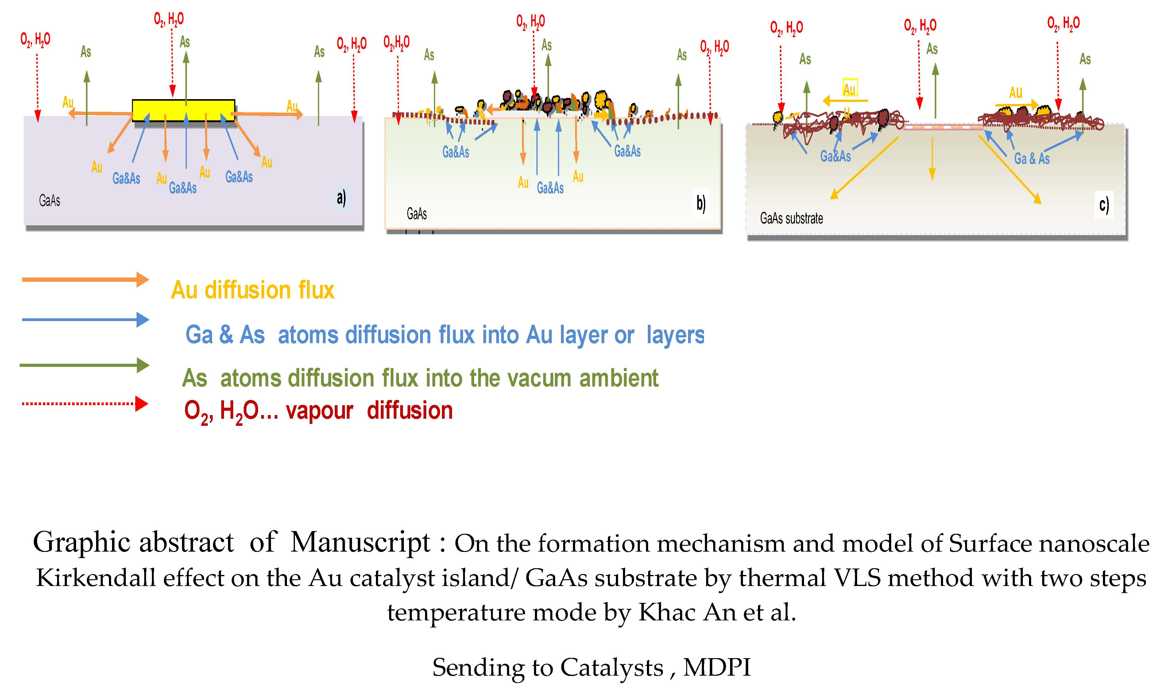
| S9 | 1000 | 410 | 20 | 620 | 30 | ~ 900 | 4.50 × 10⁻¹⁰ | Figure 1 |
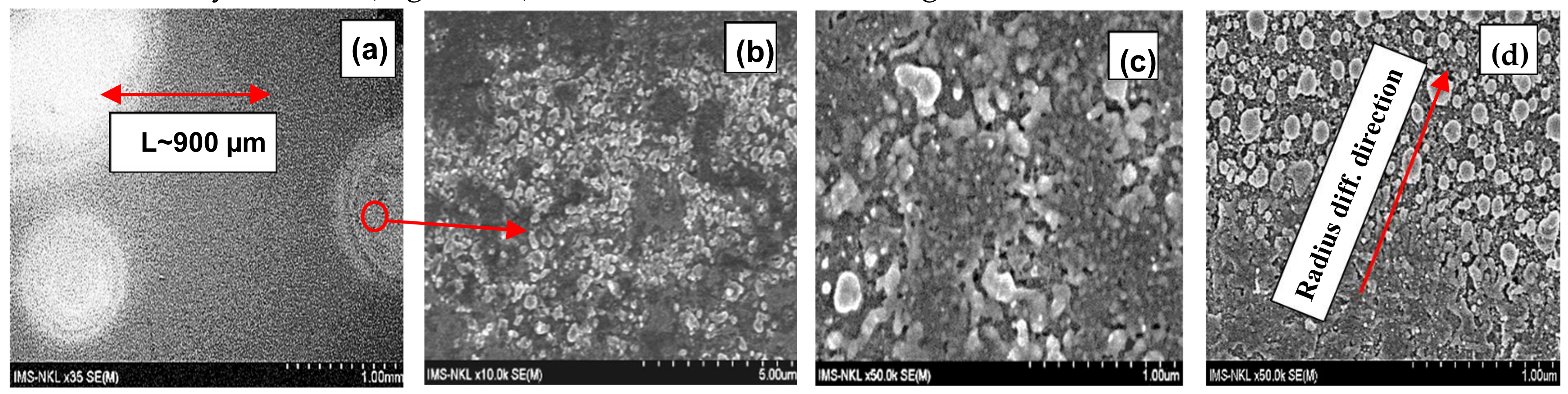
| S10 | 1000 | 440 | 20 | 640 | 30 | ~ 1300 | 9.40 × 10⁻¹⁰ | Figure 2 |
| S7 | 70 | 410 | 20 | 650 | 90 | ~ 290 | 1.567 × 10⁻¹¹ | Figure 3 |
© 2019 by the authors. Licensee MDPI, Basel, Switzerland. This article is an open access article distributed under the terms and conditions of the Creative Commons Attribution (CC BY) license (http://creativecommons.org/licenses/by/4.0/).
Share and Cite
DAO, K.A.; Pham, H.T.; Nguyen, T.T.; Phan, A.T. The Formation Mechanism and Model of the Surface Nanoscale Kirkendall Effect on Au Catalyst Island/GaAs Substrate by Thermal Vapor-Liquid-Solid Method with Two-Step Temperature Mode. Catalysts 2019, 9, 1072. https://doi.org/10.3390/catal9121072
DAO KA, Pham HT, Nguyen TT, Phan AT. The Formation Mechanism and Model of the Surface Nanoscale Kirkendall Effect on Au Catalyst Island/GaAs Substrate by Thermal Vapor-Liquid-Solid Method with Two-Step Temperature Mode. Catalysts. 2019; 9(12):1072. https://doi.org/10.3390/catal9121072
Chicago/Turabian StyleDAO, Khac An, Hong Trang Pham, Tien Thanh Nguyen, and Anh Tuan Phan. 2019. "The Formation Mechanism and Model of the Surface Nanoscale Kirkendall Effect on Au Catalyst Island/GaAs Substrate by Thermal Vapor-Liquid-Solid Method with Two-Step Temperature Mode" Catalysts 9, no. 12: 1072. https://doi.org/10.3390/catal9121072
APA StyleDAO, K. A., Pham, H. T., Nguyen, T. T., & Phan, A. T. (2019). The Formation Mechanism and Model of the Surface Nanoscale Kirkendall Effect on Au Catalyst Island/GaAs Substrate by Thermal Vapor-Liquid-Solid Method with Two-Step Temperature Mode. Catalysts, 9(12), 1072. https://doi.org/10.3390/catal9121072