Article

The Effect of Vacuum Annealing on the Structural, Electric, and Optical Properties, and Photocatalytic Activities of Sputtered TiO2 and Nb-Doped TiO2 Films

State Key Laboratory of Silicate Materials for Architectures, Wuhan University of Technology, Wuhan 430070, China
*
Author to whom correspondence should be addressed.
Catalysts 2025, 15(2), 166; https://doi.org/10.3390/catal15020166
Submission received: 16 December 2024 / Revised: 26 January 2025 / Accepted: 31 January 2025 / Published: 11 February 2025
(This article belongs to the Special Issue TiO2 Photocatalysts: Design, Optimization and Application)

Abstract

:
TiO2 is still a prototype material in photocatalytic studies. The defects, including the intrinsic and foreign defects, are reported to be important in determining the TiO2 photocatalytic properties. In the current research, amorphous TiO2- and Nb-doped TiO2 (NTO) films were firstly prepared through magnetron sputtering, which were then heated under vacuum. The as-deposited TiO2 and NTO films were amorphous, and transferred to anatase after heating. The vacuum heating at a higher temperature caused an obvious reduction in TiO2 films, and the NTO film was more prone to be reduced as Nb dopants decreased the thermal stability of the TiO2 lattice. The structure change induced by vacuum annealing had a great effect on electric and optical properties. The conductivity of the NTO films was 10,000 times and 100 times higher than that of the undoped TiO2 films after post-vacuum heating at 450 °C and 650 °C, respectively. In addition to an increase in the band tail absorption, the NTO films presented strong free-electron absorption after vacuum heating; this means that the NTO films presented a clear Bornstein moss shift after vacuum heating because of the high conduction electron density. The change in the photoinduced absorption spectra revealed a possible result that photo-induced electrons can be also trapped at Nb sites, indicating that the Nb-related defect forms deep gap states; this greatly limits the photo-induced electron interfacial transfer. The results showed that the photocatalytic degradation of methylene blue decreased after vacuum heating.

1. Introduction

Since the discovery of the Honda–Fujishima effect in 1972 [1], significant efforts have been made to utilize photocatalysis as an environmentally friendly process for addressing energy and environmental issues. Over the past few decades, it has been extensively studied in organic synthesis [2,3], carbon dioxide reduction [4,5], water reduction [6,7], etc., remaining one of the hottest research topics globally. Many materials, including organics, inorganics, metals, and metal–organic complexes, can be used as photocatalysts [8,9,10,11,12]. Among them, TiO2, one of the earliest and most typical photocatalysts studied, has continued to attract attention due to its chemical stability and low cost; it is also commonly used as a model material for studying photocatalytic mechanisms.
The photocatalytic activity of TiO2 is relatively low, great efforts have been taken to change TiO2 structure in order to change the photocatalytic activities [13,14,15,16]. For instance, Li et al. co-deposited CuOx clusters and Pt nanoparticles to facilitate photo-induced holes and electron transfers, achieving a high yield of C2 products with high selectivity [17]; Wang et al. prepared a Cuδ+/CeO2-TiO2 photocatalyst featuring atomically dispersed Cuδ+ sites anchored on the CeO2-TiO2 heterostructures that exhibited a very highly selective (75%) reduction of CO2 to C2H4 [18]; Bhattacharyya et al. doped Cu elements in TiO2 to increase photocatalytic reduction of CO2 to CH4 owing to the electronegative surface Cu1+ and O vacancies [19]; Wang et al. utilized an innovative alcohol solution plasma approach to induce the surface amorphization of TiO2 materials and reduce surface oxygen vacancies, resulting in a significant increase in photocatalytic H2 generation by 124 times due to the reduction in surface deep electron traps [20]. These studies demonstrate that altering and modifying the photo-induced charge carrier kinetics is the primary means to enhance the photocatalytic activities of TiO2 materials.
As a donor-type dopant, the Nb element has been extensively doped into the TiO2 lattice to create transparent conductive coatings [21,22,23,24]; Nb-doped TiO2 (NTO) materials have also been studied as photocatalysts. Zhang et al. prepared NTO microspheres using the ultrasonic spray pyrolysis of peroxide precursor solutions; the materials exhibited increased visible photocatalytic activities but decreased UV photocatalytic activities, attributed to the fact that the Ti3+ defects formed could increase the charge recombination [25]. Kato et al. studied the effect of Nb doping on rutile TiO2 single crystals and also found that Nb doping decreased the photocatalytic water splitting due to the increased recombination [26]; Miyagi et al. also demonstrated that NTO films displayed lower photocatalytic activity owing to the formation of deep energy levels caused by Nb ions [27]. In comparison to powders, NTO films were also prepared using different methods, including the sol-gel method [28], magnetron sputtering [29], atomic layer deposition [30], and chemical vapor deposition [31]. For example, Mattsson et al. used the sol-gel method to prepare NTO films and found that acetone degradation under solar light illumination was significantly decreased due to increased recombination caused by the formation of Nb=O clusters and cation vacancies [32]; however, Yang et al. used magnetron sputtering to prepare Nb-doped TiO2 films and showed an increase in the photocatalytic performance of anatase TiO2 due to its ability to absorb the entire visible light spectrum and efficient charge transfer [33].
TiO2-based films deposited on glazes are used for their self-cleaning function. Magnetron sputtering is an extensively used industrial way to prepare film over glazes. However, the films have been less studied relative to the powder TiO2 due to their lower photocatalytic activities. From this viewpoint, further studying sputtered TiO2-based films and their photocatalytic activities is still meaningful to guide the fabrication of self-cleaning films. The film structure, such as defects, determines photocatalytic property by changing the electron transfer kinetics and pathways. Vacuum heating has been widely used to treat sputtered NTO films in some studies [34,35,36,37,38], with electric resistivities being mainly studied because NTO films have been treated as transparent conductive oxide (TCO) films. For instance, Sato et al. firstly prepared NTO films on unheated glass substrates using magnetron sputtering, and subsequently underwent vacuum annealing, which achieved a resistivity of 6.3 × 10⁻⁴ Ω·cm and a transmittance of 60–80% in the visible-light region [35]. The effect of vacuum heating on the NTO film structure and charge kinetics, as well as their relation to the photocatalytic properties was not well investigated.
In the current research, undoped and NTO films were firstly deposited onto quartz substrates by r.f. magnetron sputtering, and subsequently subject to annealing under vacuum. The impact of vacuum annealing on the film structures, electrical properties, and optical properties was carefully studied, based on which the comprehensive effect on the film structures was analyzed. Furthermore, the in situ photoconductance and photo-induced absorption spectroscopic measurement were combined to study the charge carrier kinetics, which showed that the vacuum annealing changed the charge kinetics for both undoped TiO2 and NTO films, and the annealed NTO films shows a much slower electron interfacial transfer to O2. Lastly, the photocatalytic activities of these films were studied by degrading the methylene blue (MB). The formation of Nb-dopant-induced defects reduced the photocatalytic degradation of methylene blue under UV light illumination, indicating that vacuum-annealing-induced defects form recombination centers for both undoped and Nb-doped TiO2, in agreement with other studies [25,27].

2. Results and Discussion

2.1. Structure Analysis
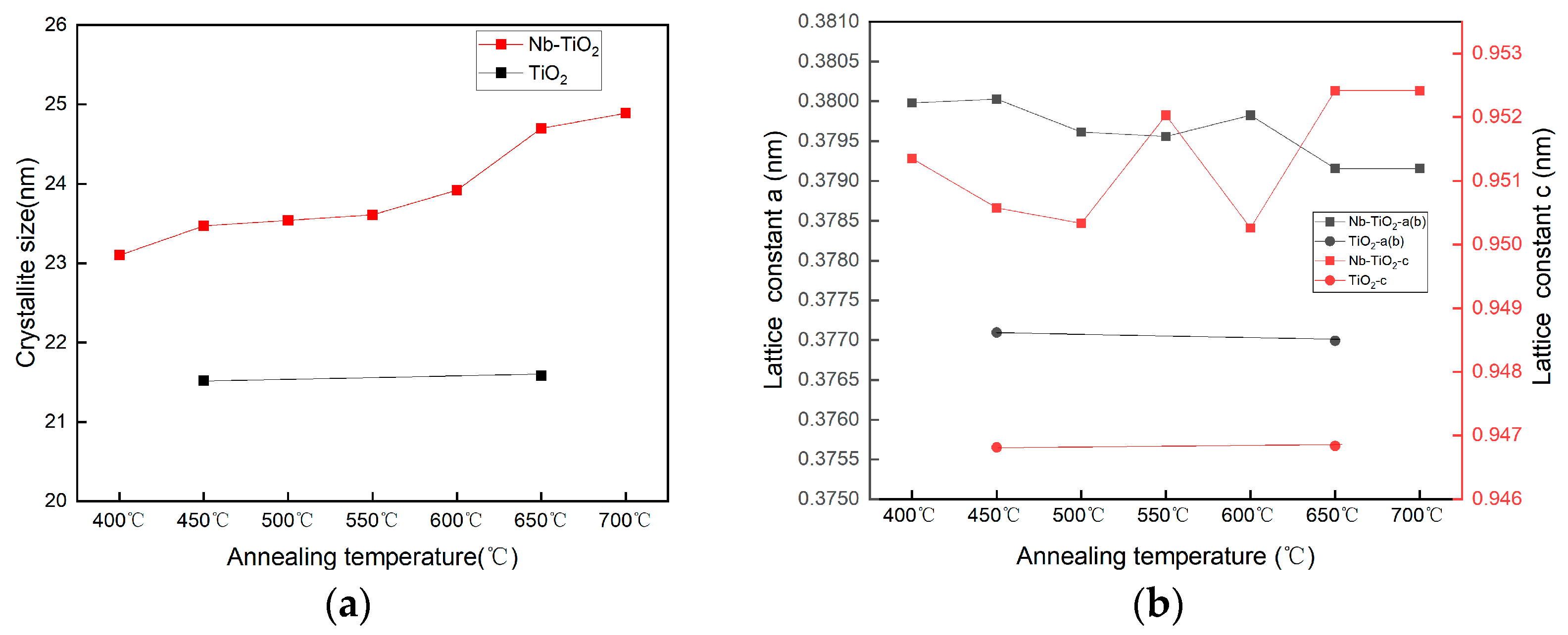
2.1.1. XRD Analysis

Figure 1a shows the XRD patterns of the as-deposited undoped TiO2 films and the films annealed at 450 °C to 650 °C. It is evident that the film deposited is amorphous, whereas the films annealed exhibit a pure anatase phase. Furthermore, as the annealing temperature raised, the film crystallinity tended to increases. Figure 1b shows the XRD patterns of the as-deposited NTO films and the films annealed at different temperatures. Similarly, the directly deposited film is amorphous, and the annealed samples exhibit anatase phase regardless of annealing temperatures. Apart from the characteristic anatase (TiO2) peaks, no other peaks corresponding to metallic Nb, Nb2O5, Ti or other TiO2 polymorphs (rutile or brookite) were observed, suggesting that the post-annealed films were of a single phase [39]. When the annealing temperature was 400 °C, the NTO film just showed very weak peaks. As the annealing temperature increased to 450 °C, the intensity of diffraction peaks increased, indicating an improvement in the film’s crystallinity. However, as the annealing temperature reached 500 °C, the peak intensities slightly decreased, suggesting a gradual decline in the film’s crystallinity due to Nb doping. This might be explained by the migration of some Nb atoms to interstitial positions or grain boundaries at higher annealing temperatures, leading to a reduction in crystallinity [40,41,42]; it is also possible that the decrease is related to the formation of more oxygen defects. Between 500 and 700 °C, the intensity of the (101) diffraction peak almost remained unchanged, suggesting a stable lattice structure under these annealing conditions.
In comparison to undoped TiO2 films, it was seen that the (101) diffraction peak of the NTO films slightly shifted to lower diffraction angles; this shift is attributed to the larger atomic radius of Nb compared to Ti, resulting in increased atomic spacing [43]. It also indirectly indicates that the Nb atoms have been effectively doped into TiO2 [44]. Furthermore, the doping of the Nb element induced a shift in the preferential orientation of the TiO2 films, from the (004) orientation in pure TiO2 films to the (101) orientation in Nb-doped TiO2 films, which also provides further evidence that Nb has been effectively incorporated into the TiO2 lattice.
Based on the Scherrer equation [45],
D   =   k λ / β cos θ
where k is the Scherrer constant (0.89), λ is the X-ray wavelength (1.54059 Å), β is the half-width of the XRD peak, and θ is the diffraction angle. Applying the Scherrer equation on the (101) peaks, the average grain sizes of the undoped and NTO films annealed at different temperatures were estimated, as shown in Figure 2a; the grain size of the Nb-TiO2 film tended to increase as the annealing temperature increased. However, the grain size of the pure TiO2 film almost remained unchanged. This indicates that Nb dopants decreased the thermal stability of the TiO2 lattice. The grains size of the Nb-doped sample was slightly larger than that of the undoped sample, which is consistent with the XRD analysis. Anatase TiO2 belongs to the tetragonal crystal system, based on the following equation [46]:
d = h 2 + k 2 a 2 + l 2 c 2 1 / 2
where d is the lattice distance; h, k, and l are the lattice plane indexes; and (a), (b), and c are the cell constants. Figure 2b shows the a and c of the undoped TiO2 and NTO films annealed at different temperatures. It was seen that the Nb doping enlarged the length of both the a and c axes, meaning that Nb should replace the lattice Ti ions or enter the interstitial sites [47].

2.1.2. FE-SEM Analysis

Figure 3 shows the FE-SEM images of the as-deposited undoped TiO2 and NTO films and the films annealed at 650 °C, respectively, with the cross-sectional FE-SEM image being shown in the upper right corner. As can be seen from Figure 3a,c, both the as-deposited TiO2 and NTO films show dense and smooth surfaces. However, the annealed samples exhibited a relatively uneven surface containing many irregular interconnected nanoparticles. The annealed undoped TiO2 film also contained cracks; in contrast, the annealed NTO film had no cracks. This indicates that the doping of Nb enables the film to better withstand thermal and internal stresses during the annealing process, thereby preventing cracking. Based on the cross-section images, the thicknesses of unheated TiO2 and NTO films were 227 nm and 293 nm, respectively, and the thicknesses of the heated TiO2 and NTO films were 250 nm and 287 nm, respectively.

2.1.3. Raman Analysis
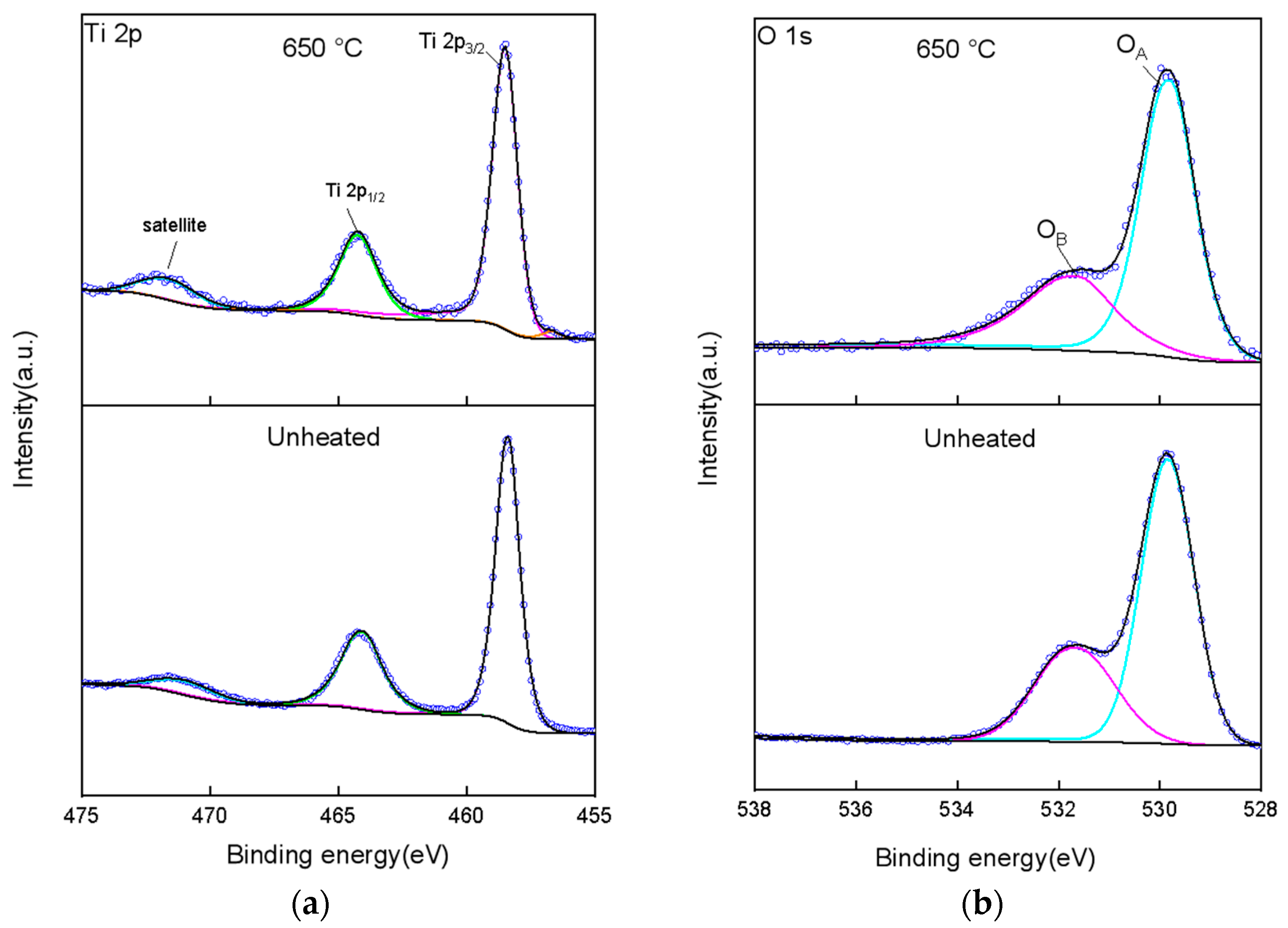
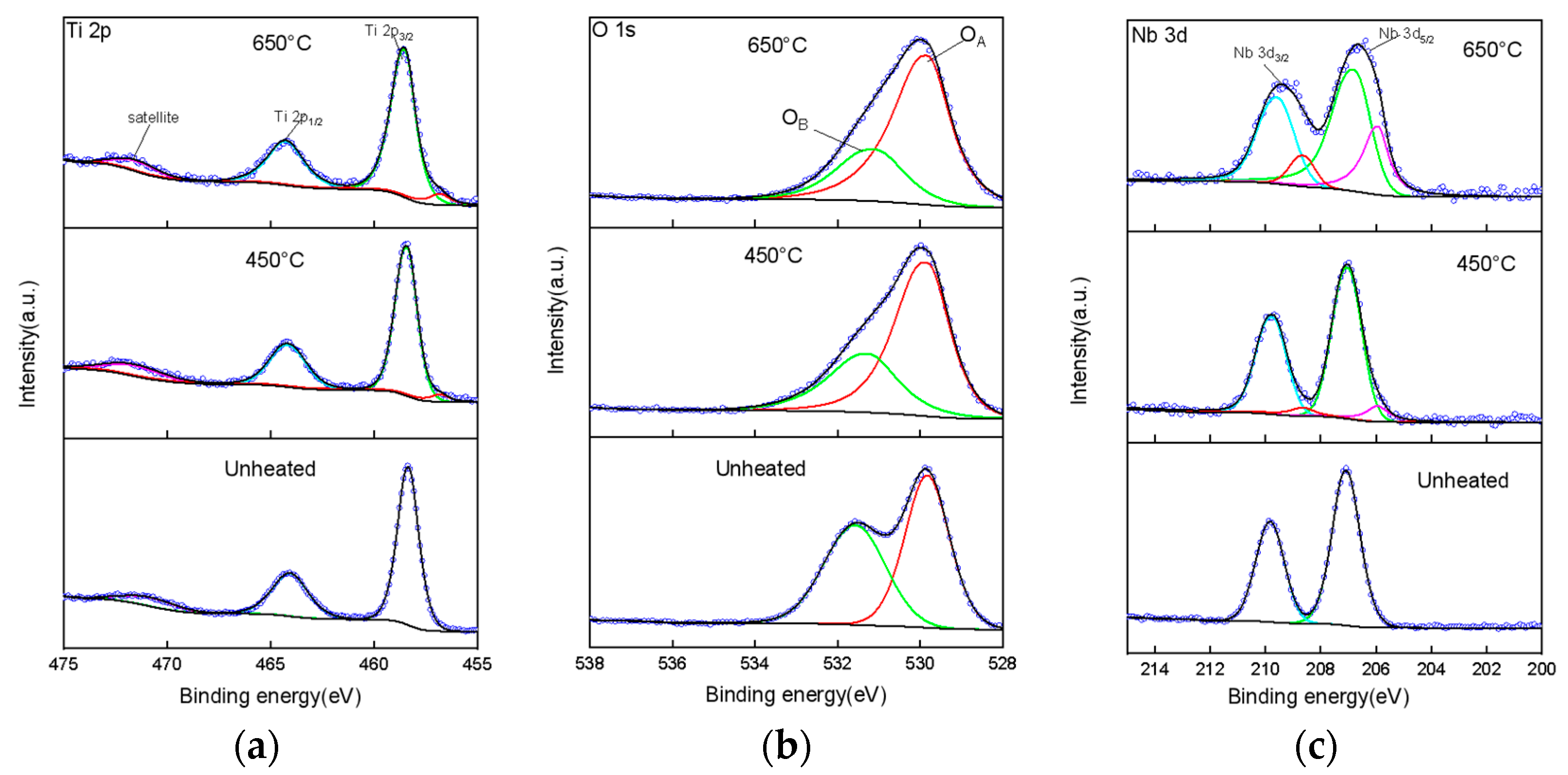
Figure 4a shows the Raman spectra of the as-deposited undoped TiO2 films and the films annealed at different temperatures. It can be seen that the as-deposited TiO2 film does not show distinct characteristic peaks, while the TiO2 films annealed show characteristic peaks of the anatase phase. As the annealing temperature increases from 450 °C to 650 °C, the Eg peaks slightly shift toward lower frequencies, with its intensity increasing with heating temperatures. This shows that the TiO2 film crystallinity improved as the annealing temperatures increased, in consistence with the XRD analysis [48,49]. Figure 4b shows the Raman spectra of NTO films annealed at different temperatures. Similarly, the annealed NTO films exhibited characteristic peaks of the anatase phase, while the unheated sample did not. When the annealing temperature ranged from 400 °C to 550 °C, it was seen that the Eg peak almost remained at 153 cm−1; when the annealing temperature was higher than 550 °C, this peak slightly shifted toward higher frequencies. Currently, there are three primary mechanisms that can explain the shift in Raman peaks: phonon confinement effect, stress, and non-stoichiometric equilibrium resulting from oxygen deficiency. Stress effects typically induce larger Raman peak shifts, with the Raman peaks shifting toward lower frequencies as stress increases [50,51]. Additionally, stress arising from size effects can also influence Raman peaks, when larger nanoparticles generate a more significant pressure effect, leading the Raman peaks to shift toward lower frequencies [52]. In our experiment, the size of TiO2 nanoparticles gradually increased as the annealing temperature rises. Therefore, according to the mechanism of the stress effects due to size, the Eg Raman peak of TiO2 are expected to shift toward lower frequencies. However, in the actual Raman spectra obtained from the experiment, the Eg Raman peak shifted toward higher frequencies as the annealing temperature increased. Therefore, stress effects were not the cause of the change in Raman peak position here. Considering that the annealing method used in this experiment was under vacuum, the influence of oxygen defects needs to be taken into account. According to the literature reports [50,51,52], the Eg peak shifted toward higher frequencies as the concentration of oxygen defects increased, accompanied by a decrease in Raman peak intensity. Therefore, it was concluded that as the annealing temperature raised, the oxygen defect concentration increased, leading to a shift in the Eg Raman peak toward higher frequencies and a reduction in peak intensity.

2.1.4. XPS Analysis

Figure 5a,b shows the XPS spectra of Ti 2p and O 1s for as-deposited and heated TiO2 film, respectively. It can be seen from Figure 5a that the Ti 2p3/2 and Ti 2p1/2 peaks appear at 458.4 eV and 464.1 eV, respectively, which align with the binding energies of undoped TiO2 reported in the literature, confirming the presence of Ti4+ ions [53]. For the TiO2 film annealed at 650 °C, the peaks at 458.51 eV and 464.25 eV are also present for the Ti4+ in TiO2. In addition, a weak peak at 456.7 eV also appeared due to the Ti3+ formation; it ascribes to vacuum annealing conditions which may induce electron transfer processes from oxygen vacancies to Ti4+ ions, thus leading to the occurrence of reduced Ti3+ ions [54]. The atomic percentage of the Ti3+ was 1.5 at.%. The O 1s spectra consisted of two peaks, labeled OA and OB. OA, located at 529.8 eV, corresponds to lattice O2− ions in anatase; OB, situated at 531.7 eV, is attributed to hydroxyl groups or physical adsorbed water molecule [55]. The hydroxyl group percentage remained around 31% before and after vacuum annealing.
Figure 6a–c shows the high-resolution core-level XPS spectra of Ti 2p, Nb 3d, and O 1s for the as-deposited NTO films and the films annealed at 450 °C and 650 °C, respectively. It can also be seen from Figure 6a that the Ti 2p3/2 and Ti 2p1/2 peaks appear at 458.34 eV and 464.06 eV, confirming the presence of Ti4+ ions. For the NTO film annealed at 450 and 650 °C, the peaks at 456.80 eV and 456.83 eV represent the presence of Ti3+. The result shows that the chemical valence state of the Ti element in the as-deposited sample is tetravalent, while Ti3+ ions were also present for annealed sample. The atomic percentages of Ti3+ in the films annealed at 450 °C and 650 °C were 5.0% and 6.3%; this is much higher than that in the pure film annealed at 650 °C. It can also be seen from Figure 6c that the Nb3d3/2 and Nb3d5/2 peaks appeared at 207.07 eV and 209.83 eV, confirming the presence of Nb5+ ions [56]. For the NTO film annealed at 450 and 650 °C, the peaks at 205.95 eV, 208.652 eV, 205.92 eV, and 208.62 eV represent the presence of Nb4+ [57]. The result shows that the Nb chemical state of the as-deposited film was pentavalent, and the Nb4+ states also appeared for the annealed films. The atomic percentages of the Nb4+ were 11% and 25% for the NTO films annealed at 450 °C and 650 °C, respectively. The increased Ti3+ ions and the appearance of Nb4+ means that the NTO film were subject to easier reductions under vacuum annealing compared to the undoped film. The O 1s spectra show that the content of the hydroxyl groups (O) of the as-deposited film was higher than that in the undoped one, which was 47 at.%. After vacuum annealing, the hydroxyl group content decreased to around 25%, and the envelope of the O1s XPS spectra became much different from that of the undoped film. The above result means that the vacuum annealing had a bigger effect on the structure of NTO films. In general, the reduction in Ti and Nb ions by vacuum annealing was caused by the formation of oxygen vacancies. These oxygen vacancies donate electrons to TiO₂ lattice, thereby reducing the Ti and Nb ions. As a result, it is understood that Nb doping decreased the thermal stability of the TiO₂ structure, and the NTO films exhibited a tendency to form more oxygen vacancies in addition to the presence of Nb dopants.

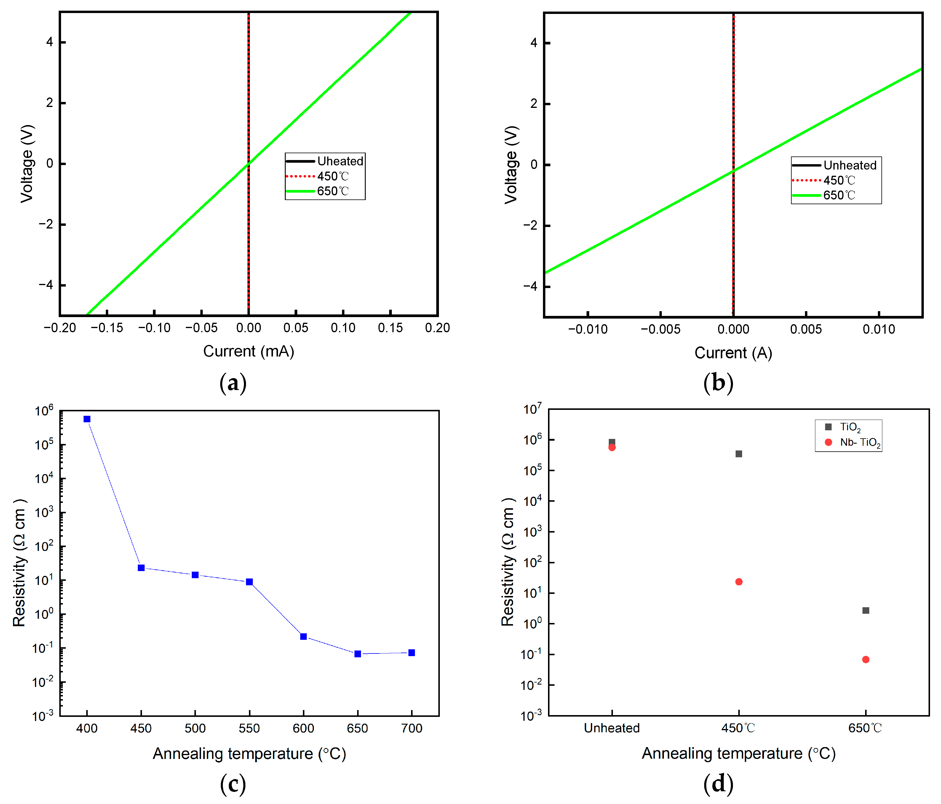
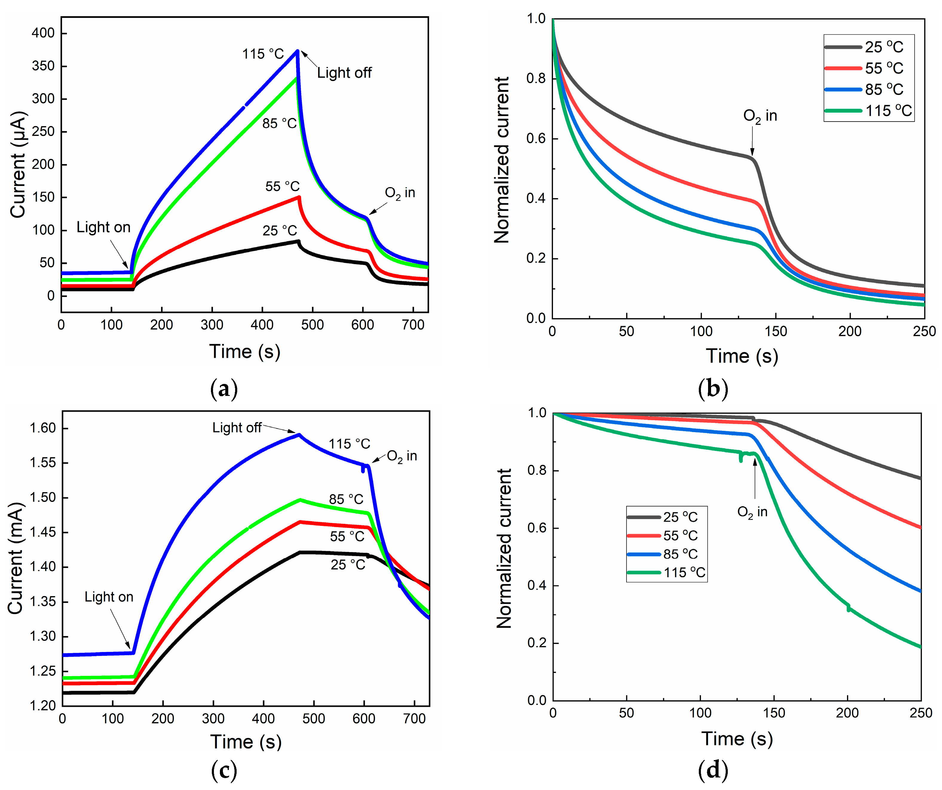
2.2. Electric Property Analysis

Figure 7a shows the linear voltage–current (V-I) curves of the unheated TiO2 films and the films after vacuum annealing at 450 and 650 °C, which were all measured at 15 °C. It can be seen that they all exhibited typical Ohmic behaviors, and the slopes are the electric resistances, based on which the film resistivities were calculated. The resistivities of the unheated and TiO2 films after vacuum heating at 450 and 650 °C were 8.2 × 10⁵ Ω·cm, 3.4 × 10⁵ Ω·cm, and 2.7 Ω·cm, respectively. It is evident that the vacuum heating at 650 °C leads to the significant decrease in resistivities; this is attributed to the formation of oxygen defects that act as conductance donors, as revealed in the XPS analysis. The linear V-I plots of the unheated NTO film and the films after vacuum annealing at 450 °C and 650 °C are shown in Figure 7b; they also exhibited Ohmic behaviors. From their slopes, the NTO film resistivities were obtained. Figure 7c shows the resistivities of the NTO films after vacuum heating at different temperatures. Specifically, the resistivity of the as-deposited NTO film was 5.6 × 10⁵ Ω·cm, which remained largely unchanged after 400 °C vacuum heating (5.7 × 10⁵ Ω·cm). However, as the vacuum heating temperature increased to 450 °C, the resistivity dropped significantly to 23.4 Ω·cm, further decreasing to ~6.8 × 10⁻² Ω·cm when the annealing temperature was increased to 650 °C. Figure 7d compares the resistivities of undoped TiO2 and NTO films for unheated and heated samples. It was seen that Nb doping did not reduce the resistivity of the as-deposited film; however, after vacuum heating at 450 °C, the NTO film exhibited resistivity 104 times lower than that of the undoped film. When the heating temperature was 650 °C, Nb doping still reduced the resistivity ~100 times. Therefore, it is known that Nb doping enables the formation of more donor-type defects in TiO2 films, consistent with XPS analysis findings.
Figure 8a shows the photocurrent responses of unheated TiO2 and NTO films under and subsequent to 375 nm laser illumination. Under laser irradiation, both samples exhibited an initial rapid increase in photocurrents, followed by a gradual slowdown. Upon the cessation of laser illumination, a similar pattern was also observed, with an initial swift drop-off and gradual relaxation. This photocurrent behavior likely stems from the amorphous disorder, specifically the filling and subsequent depletion of disorder-induced traps. As the photocurrent rise and relaxation patterns of the NTO film closely resembled those of the undoped sample, it was surmised that the Nb doping into the as-deposited TiO2 lattice should be insufficient, thus having a limited effect on the photocurrent responses. This finding aligns with the observation that the resistivity of the Nb-doped film is nearly identical to that of the undoped film.
Figure 8b shows the photocurrents of undoped and NTO films that have undergone annealing at 650 °C under and after 375 nm laser illumination. Notably, the photocurrent behavior differed significantly from that of the unannealed films. Firstly, the photocurrent of both films significantly enhanced, attributed to the transition from amorphous to crystalline structures, which likely increased electron mobility and density. Secondly, the photo current increased steadily until it reached a stable value under laser illumination, with no clear distinction between the fast and slow component. After the laser was turned off, both samples experienced a continuous relaxation, but the relaxation of the NTO was significantly slower, exhibiting a much slower persistent relaxation under the measurement conditions; this means that Nb-induced defects have a substantial influence on the kinetics of photo-induced electrons.
Figure 9a shows the photo currents of the undoped TiO2 films measured at different temperatures. It was seen that the dark currents increased with temperatures because of the heat activation of the electrons to the conduction band. The photo current increased as the temperature increased; this means that the high temperature can help increase the accumulation of photo-induced electrons in TiO2. Figure 9b shows normalized photocurrent relaxation after the laser illumination; the relaxation rate increased with temperatures, indicating that the relaxation featured thermal activation. The O2 introduction resulted in an obvious increase in the relaxation; this means that the photocurrent relaxation is related with the chemisorption of O2 over the TiO2 surface, accompanied by the electron transfer from TiO2 to O2 [58]. Figure 9c shows the photocurrent responses of the NTO film measured at various temperatures, and the dark current increased with temperatures. Under laser illumination, the photo currents increased as the temperature increased. However, the increase behaviors became different from that of the undoped TiO2 films, meaning that Nb doping affects the kinetics of the photo-induced electrons. Figure 9d shows the normalized photocurrent relaxations after the end of laser illumination, and it can be seen that the relaxation rate is much lower than that of the undoped films at all temperatures. Furthermore, the relaxations increased with temperatures, and the O2 introduction increased the photocurrent relaxation, which also increased with temperatures; this was different from that of the undoped films. Therefore, the above photocurrent results clearly revealed that the photocurrent relaxation related to the electron-assisted O2 chemisorption over the TiO2 surface. However, especially at an ambient temperature, Nb doping greatly reduced the electron transfer rate.

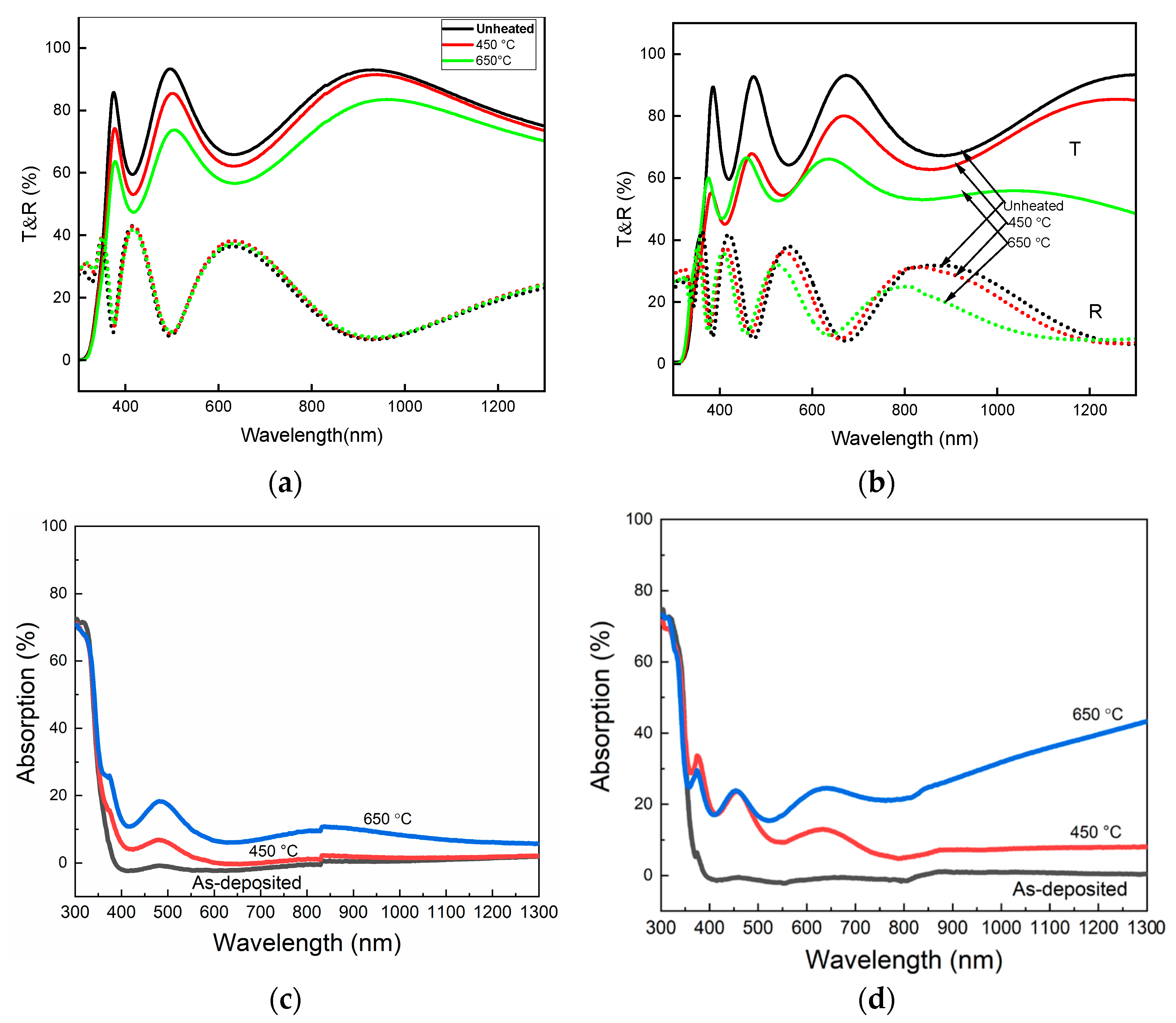
2.3. Optical Property Analysis

Figure 10a shows the transmittance and reflectance spectra of the as-deposited undoped TiO2 and that heated at 450 °C and 650 °C; they all show obvious interference wavy behaviors because of the large difference in TiO2 and quartz refractive indexes (about 2.4 at 550 nm for TiO2 and about 1.47 for quartz glass at 550 nm). It was seen that the entire transmittance spectrum exhibited a slight drop after heating at 450 °C, and a more significant decrease was noted when the temperature was increased to 650 °C. Conversely, the reflectance spectra almost remained unchanged after vacuum heating, regardless of the temperatures. Figure 10b shows the transmittance and reflectance spectra of the NTO films before and after heating at 450 °C and 650 °C. Notably, the transmittance spectra underwent a more substantial decrease after vacuum heating compared to the undoped samples. Specifically, when the vacuum heating temperature was 650 °C, the transmittance spectra in the near-infrared wavelength region decreased significantly relative to that annealed at 450 °C. The vacuum annealing at 450 °C had a minor effect on the reflectance spectra, whereas a more significant change was caused by the annealing at 650 °C.
Figure 10c shows the absorption spectra (1-R-T) of the undoped TiO2 films. It was seen that the unheated film almost exhibited no absorption above the optical threshold (~400 nm), while the sample annealed at 450 °C showed distinct band tail absorption up to 600 nm, which arised from oxygen defects and the lattice disorder. When the heating temperature was 650 °C, in addition to the increased band tail absorption, a broad absorption was also present throughout the near-infrared regions; this is attributed to the presence of Ti3+ ions, consistent with the XPS analysis. Figure 10d shows the absorption spectra of the NTO films. The unheated sample lacked absorption above the optical threshold. Upon vacuum heating at 450 °C, the NTO film exhibited higher band tail absorption compared to the unheated film, indicating that more oxygen defects and lattice disorder were created. Furthermore, the presence of Nb4+ and Ti3+ ions also contributed to the broad absorption in the near-infrared region. When the heating temperature was increased to 650 °C, it was seen that the band tail absorption almost remained unchanged, but a significant increase in the near-infrared absorption was revealed. This absorption exhibited a near-monotonic increase with wavelengths, signifying free-electron absorption [59]; this observation is in line with the resistivity measurement as well. Therefore, the above comparison clearly revealed that the vacuum heating had more effect on the optical proprieties of the NTO films because more defects were generated.
In the case of the indirect transition mechanism (anatase TiO2), the absorption coefficients near the optical threshold related with the photon energy through
α · h ν 1 / 2 h ν
Where α, h, and ν are the absorption coefficient, Planck constant, and light frequency [60]. Based on this, the optical Eg energies could be obtained through the extrapolation method. The absorption coefficient (α) of the films was simply calculated through
α λ = 1 d ln 1 R λ T λ
where d is the film thickness (obtained from the FE-SEM image (Figure 2), and R(λ) and T(λ) are the measured reflectance and transmittance at wavelength of λ [61]. Figure 11a shows the dependence of (αhν)1/2 on hν for undoped TiO2 films; this clearly shows that vacuum heating had no effect on the Eg energies, which was ~3.34–3.36 eV for all the samples. Figure 11b shows the dependence of (αhν)1/2 on hν for the NTO films, based on which the Eg energies of unheated NTO film and the films heated 450 °C and 650 °C were determined to be 3.32 eV, 3.38 eV, and 3.48 eV, respectively. The 3.48 eV of Eg should be ascribed to the Bornstein moss effect because of the filling electrons in the TiO2 CB [62]. The Bornstein moss shift of Eg can be estimated according to the following equation [63]:
Δ E g = h 2 N 2 3 / ( 8 m * π 3 2 3 )
where N is the conduction band electron density and m* is the effective mass of the electron locating at the CBM. The carrier density of the Nb-TiO2 prepared from vacuum heating at 650 °C was also determined by the Hall measurement, which was 1.7 × 1019 cm−3. The Eg of the undoped TiO2-650 °C was 3.35 eV, which became 3.48 eV for Nb-TiO2-650 °C, so the ΔEg caused by the Bornstein moss effect was 0.13 eV and the electron effective mass (m*) was about 0.17 m0 (m0 is the mass of a free electron); this agrees with the published results [64]. Furthermore, the Hall effect measurement also shows that the electron hall mobility of NTO was 1.3 cm2 V−1s−1; this is much lower compared to the other TCO film, such FTO, GZO, and AZO, due to the impurities scattering caused by vacuum heating.
Figure 12a shows the difference (ΔT) between the UV-vis transmittance spectra of the unheated TiO2 films before and after 15 and 30 min, at 375 nm laser illumination from 450 nm to 800 nm. Here, the positive ΔT means the decrease in transmittance, mainly caused by the absorption of the films induced by light illumination. It was seen that the laser illumination leads to an absorption peak at 500 nm for undoped TiO2 film before vacuum heating, and a monotonically increased absorption in the near-infrared wavelength. The absorption peak at 500 nm was ascribed to the trapping of electrons at the disorder-induced gap states as the as-deposited TiO2 film was amorphous. The monotonically increased absorption should be ascribed to the electron accumulation at the extended states (conduction band state), which also contributes to photo-induced conductance. Figure 12b shows the ΔT between the UV-vis spectra of the TiO2 film heated at 650 °C before and after 15 and 30 min, at 375 nm laser illumination; this is completely different from that of the unheated sample. It was seen the transmittance spectrum underwent a slight increase after laser illumination, meaning that electrons are not well trapped at the gap states and accumulated in the conduction band for crystalline anatase TiO2 films, in the present case. Figure 12c shows the ΔT between the UV-vis spectra of the unheated NTO film before and after 15 and 30 min, at 375 nm laser illumination. The laser illumination resulted in wide absorption band around 630 nm, which is different from the undoped film. Therefore, it was considered that the photo-induced absorption at 630 nm might arise from electron trapping at Nb dopants. Figure 12d shows the ΔT between the UV-vis spectra of the NTO film heated at 650 °C before and after 15 and 30 min, at 375 nm laser illumination; this is also different from the undoped sample. The photo-induced peak located at 635 nm, possibly arising from electron trapping at Nb dopants, still existed; this is the same as for the unheated sample. Differently, the photo-induced absorption started to increase when the wavelength was longer than 760 nm, which might be ascribed to electrons accumulated at the Ti sites or conduction band. Although it is also possible that the photo-induced absorption might be caused by reasons other than the above assignment, the large difference between the undoped and NTO film shows that the Nb-dopant-induced defect must alter electron trapping and affect photo-induced electron relaxation kinetics.

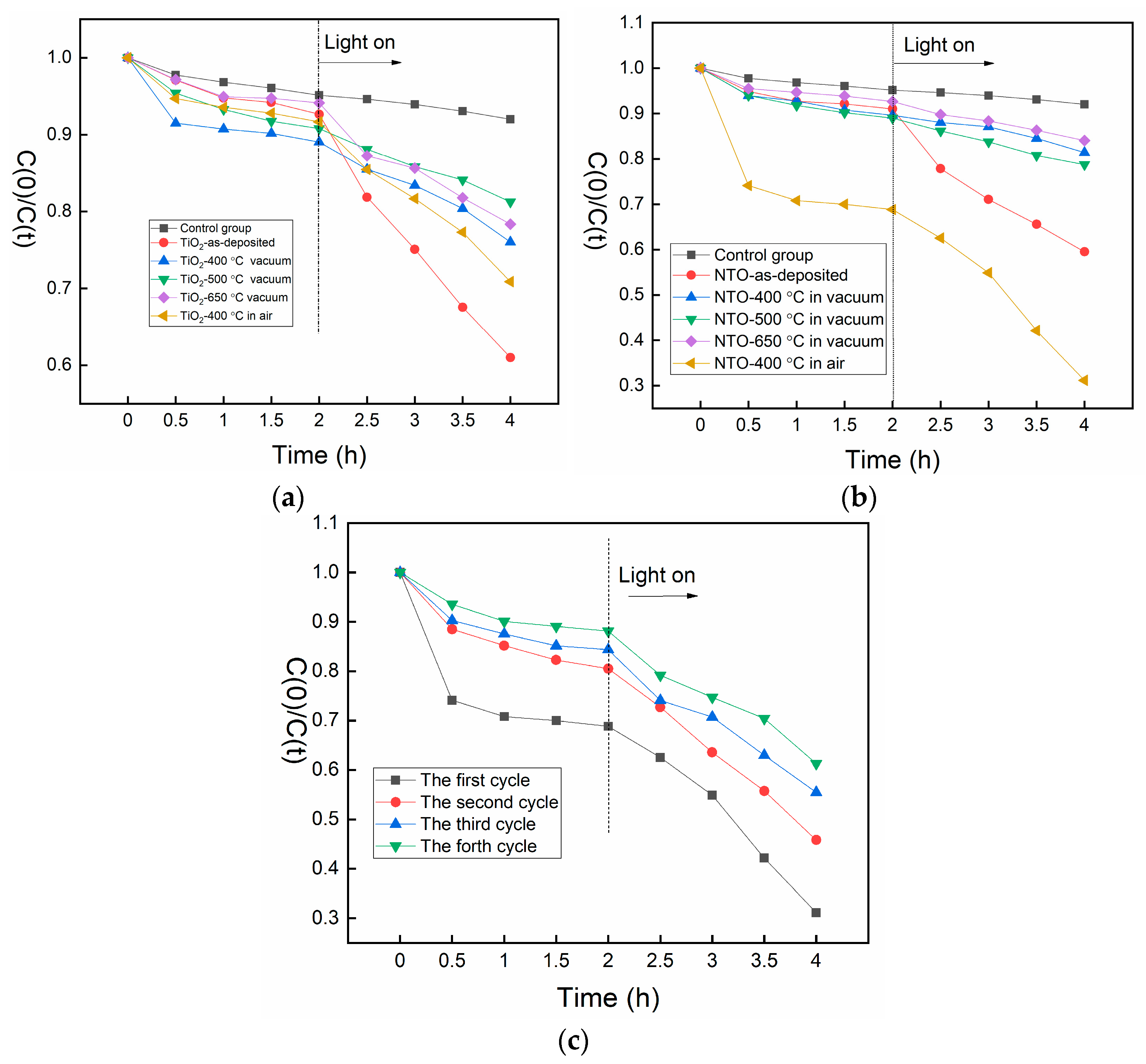
2.4. Photocatalytic Performance Analysis

The photo-induced degradation of aqueous methylene blue (MB) solutions was used to evaluate the photocatalytic activities. The concentrations of MB aqueous solutions were firstly measured per 30 min in the dark for 2 h and were then measured for another 2 h under light illumination. Figure 13a shows that the C(0)/C(t) (C(0) is the initial concentration, and C(t) is the aqueous concentration at time t) of the aqueous MB solution for the undoped film, as well as the films after vacuum heating at 400 °C, 500 °C, and 650 °C; the film after annealing in air at 450 °C was also compared. Compared to the control test (without using TiO2), the unheated and heated films showed enhanced MB adsorption, and they all showed photocatalytic activities under light illumination. It was unexpected that the undoped film had the highest activity, which was decreased after annealing under vacuum and in air. The photocatalytic activity after annealing in air was slightly higher than that after annealing under vacuum. Figure 13b shows the C(0)/C(t) of the aqueous MB solution for the NTO films. In this case, the NTO film annealed in air showed the highest adsorption in the dark, and it also had the highest photocatalytic activity. The as-deposited NTO film showed weak MB adsorption ability, and its photocatalytic activity was slightly lower than that annealed in air. All of the NTO films annealed under vacuum were almost inactive. Therefore, in spite of undoped and NTO film, it can be seen that the vacuum heating greatly decreased the photocatalytic activities; this means that the vacuum heating induced defects had a negative effect on photocatalytic effects, and the Nb doping led to further a decrease in photocatalytic activity. The above optical and electric analysis revealed that the vacuum heating could create more defects in the film, which greatly limit the electron transfer rate; this might lead to the observed decreased photocatalytic activities, such observation was also in agreement with other studies [25,32]. The photocatalytic experiments of the NTO film after annealing in air were repeated four times, as shown in Figure 13c, and it can be seen that, although the adsorption abilities tended to decrease, while the photocatalytic activity almost remained unchanged.

3. Materials and Methods

Initially, radio frequency (RF) magnetron sputtering was employed to deposit pure TiO2 amorphous films and NTO (Nb2O5:TiO2 = 5:95 at.%, 99.9%) amorphous films on quartz glass substrates (25 mm × 25 mm × 1 mm). The target materials used were TiO2 (99.9%) and NTO ceramic targets. Before deposition, the chamber pressure was evacuated to 5 × 10⁻⁶ Torr. Using argon and oxygen as the sputtering and reactive gases, 18 sccm of argon was introduced to pre-sputter the target for 20 min before the actual sputtering process to remove surface organic matter and contaminants. During the actual sputtering, 15 sccm of argon and 0.1 sccm of oxygen were introduced, and the chamber pressure was maintained at 3 mTorr. The pure TiO2 film was deposited at an RF power of 80 W for 7 h, while the NTO film was deposited at an RF power of 100 W for 5 h. During the deposition process, the substrate was not heated. Before deposition, the quartz glass substrates were ultrasonically cleaned twice with high-purity water and alcohol, each time for 30 min. The deposited amorphous TiO2 films and amorphous NTO films were placed in an annealing furnace and underwent vacuum annealing for 1.5 h at different temperatures: 450 °C and 650 °C for the TiO2 films; and 400 °C, 450 °C, 500 °C, 550 °C, 600 °C, and 650 °C for the NTO films, all under a vacuum environment of 5 × 10⁻³ Torr.
The cross-sectional images and surface morphologies of the films were observed using a field emission scanning electron microscope (FE-SEM, S-4800, Hitachi, Tokyo, Japan). The crystal structures of the films were analyzed using a grazing incidence X-ray diffractometer (GIXRD, Empyrean, the Netherlands) with an incident angle of 0.5° and a measurement range of 0–80° at a scan speed of 5°/min, utilizing 4 KW Cu Ka radiation as the X-ray source. Raman scattering spectra were obtained using a Raman spectrometer (InVia, RENISHAW, London, England) excited by a 633 nm laser, with a wavenumber range of 100–1200 cm−1. The valence states and elemental compositions of the films were determined using X-ray photoelectron spectroscopy (XPS) (Model: VG Multilab 2000, Thermo Scientific, Waltham, America). The electrical resistances of the films were measured in a four-probe configuration using a Keithley 2450 digital source meter on an INSTEC cryostage. During the measurement, the temperature of the deposited samples was maintained at 15 °C using the INSTEC temperature control software (v1.0) by adjusting the amount of liquid nitrogen flowing through the system. Dry nitrogen was also introduced to avoid moisture formation on the sample surface. The Hall Effect Tester was employed to determine the carrier concentration and mobility of the films (HMS-7000, Ecopia company, Anyang City, South Korea). The transmittance and reflectance of different samples were tested using a UV-vis-NIR spectrophotometer (UV-2600, Shimadzu, Tokyo, Japan) equipped with an optical integration sphere in the range of 300–1300 nm to obtain the optical bandgaps of the various annealed samples.
The in situ photo currents of the unheated TiO2 and Nb-TiO2 and the films heated were measured on the cryostage with the Keithley 2450 and 7510 digital source meter in a two-probe mode at different temperatures, with the methanol-containing pure N2 continuously flowing through the measurement chamber. The 375 nm laser was used to illuminate the sample surfaces during the measurements, with the laser power kept at 300 mW. In addition, the effect of the light illumination on the transmittance spectra of these films was also measured with a self-designed measurement cell placed in a Shimadzu 2600 UV-vis spectrometer (see our previous study for reference) at ambient temperatures. The methanol-containing pure N2 continuously flowed through the measurement cell during the measurement. The UV-vis-NIR transmittance spectra before and after 15 min and 30 min of light illumination was recorded; the same 375 nm laser was used as the light source, with the laser power being kept 300 mW. Lastly, the differences between the transmittance spectra before and after the laser illumination were obtained to show the effect of light illuminations.
Photocatalytic activities of the TiO2 films were evaluated by degrading the methylene blue (MB) aqueous solution under 365 nm monochromic light illumination. A ϕ 10 cm film was put in a ϕ 12 cm glass container, with 35 mL of 10 mg/4 L MB solution being added; a quartz glass was covered over the MB-solution-containing glass container to avoid the solution evaporation during the light illumination. A Xe lamp (PLS-SXE300) equipped with a 365 nm band-passed filter was used as the light source of the photocatalytic reactions, and the light intensity being 0.5 mW/cm2. The UV-vis absorption spectra of the MB solution in the dark and under light illumination was measured every 30 min.

4. Conclusions

The result showed that both the undoped TiO2 and NTO films were changed to the anatase phase after vacuum heating. Nb doping reduced the thermal stability of the TiO2 lattice, which became easier to be reduced. The electric and optical properties were almost the same for both the undoped and NTO films, and became different after vacuum annealing. It was seen that the resistivity of the NTO films became much lower than that of undoped samples, and the NTO films also showed a higher band tail absorption below the band gap and the free-carrier absorption in the near-IR region, indicating that more defects were created by vacuum heating in the NTO films. The in situ photo-induced conductance and absorption spectra also indicated that the Nb-dopant-induced defects should form gap states for photo-induced electron trapping; this greatly decreased the electron interfacial transfer, and, as a result, the photocatalytic activity was decreased.

Author Contributions

Conceptualization, supervision, and writing—review and editing: B.L.; methodology, investigation, data curation, writing—original draft preparation, M.L. and Y.F. All authors have read and agreed to the published version of the manuscript.

Funding

This research was funded by National Key Research and Development of China (grant number 2017YFE0192600), and the 111 Project (grant number B18038), as well as and the National Natural Science Foundation of China (no. 51772230).

Data Availability Statement

The data that support the findings of this study are available from the corresponding author upon reasonable request.

Conflicts of Interest

The authors declare no conflicts of interest.

References

  1. Fujishima, A.; Honda, K. Electrochemical Photolysis of Water at a Semiconductor Electrode. Nature 1972, 238, 37–38. [Google Scholar] [CrossRef] [PubMed]
  2. Qi, M.Y.; Conte, M.; Anpo, M.; Tang, Z.R.; Xu, Y.J. Cooperative Coupling of Oxidative Organic Synthesis and Hydrogen Production over Semiconductor-Based Photocatalysts. Chem. Rev. 2021, 121, 13051–13085. [Google Scholar] [CrossRef]
  3. Schultz, D.M.; Yoon, T.P. Solar synthesis: Prospects in visible light photocatalysis. Science 2014, 343, 1239176. [Google Scholar] [CrossRef] [PubMed]
  4. Ran, J.; Jaroniec, M.; Qiao, S.Z. Cocatalysts in Semiconductor-based Photocatalytic CO2 Reduction: Achievements, Challenges, and Opportunities. Adv. Mater. 2018, 30, 1704696. [Google Scholar] [CrossRef]
  5. Fang, S.; Rahaman, M.; Bharti, J.; Reisner, E.; Robert, M.; Ozin, G.A.; Hu, Y.H. Photocatalytic CO2 reduction. Nat. Rev. Methods Primers 2023, 3, 61. [Google Scholar] [CrossRef]
  6. Ge, M.; Cai, J.; Iocozzia, J.; Cao, C.; Huang, J.; Zhang, X.; Shen, J.; Wang, S.; Zhang, S.; Zhang, K.-Q.; et al. A review of TiO2 nanostructured catalysts for sustainable H2 generation. Int. J. Hydrogen Energy 2017, 42, 8418–8449. [Google Scholar] [CrossRef]
  7. Hejazi, S.; Mohajernia, S.; Osuagwu, B.; Zoppellaro, G.; Andryskova, P.; Tomanec, O.; Kment, S.; Zboril, R.; Schmuki, P. On the Controlled Loading of Single Platinum Atoms as a Co-Catalyst on TiO2 Anatase for Optimized Photocatalytic H2 Generation. Adv. Mater. 2020, 32, 1908505. [Google Scholar] [CrossRef] [PubMed]
  8. Zhang, Y.; Liu, H.; Gao, F.; Tan, X.; Cai, Y.; Hu, B.; Huang, Q.; Fang, M.; Wang, X. Application of MOFs and COFs for photocatalysis in CO2 reduction, H2 generation, and environmental treatment. EnergyChem 2022, 4, 100078. [Google Scholar] [CrossRef]
  9. Liu, Q.; Huang, J.; Wang, L.; Yu, X.; Sun, J.; Tang, H. Unraveling the Roles of Hot Electrons and Cocatalyst toward Broad Spectrum Photocatalytic H2 Generation of g-C3N4 Nanotube. SolarRRL 2021, 5, 2000504. [Google Scholar]
  10. Yue, X.; Hou, J.; Zhao, H.; Wu, P.; Guo, Y.; Shi, Q.; Chen, L.; Peng, S.; Liu, Z.; Cao, G. Au-Ag alloy nanoparticles with tunable cavity for plasmon-enhanced photocatalytic H2 evolution. J. Energy Chem. 2020, 49, 1–7. [Google Scholar] [CrossRef]
  11. Melchionna, M.; Fornasiero, P. Updates on the Roadmap for Photocatalysis. ACS Catal. 2020, 10, 5493–5501. [Google Scholar] [CrossRef]
  12. Peiris, S.; de Silva, H.B.; Ranasinghe, K.N.; Bandara, S.V.; Perera, I.R. Recent development and future prospects of TiO2 photocatalysis. J. Chin. Chem. Soc. 2021, 68, 738–769. [Google Scholar] [CrossRef]
  13. Piątkowska, A.; Janus, M.; Szymański, K.; Mozia, S. C-,N- and S-Doped TiO2 Photocatalysts: A Review. Catalysts 2021, 11, 144. [Google Scholar] [CrossRef]
  14. Cheng, C.; Fang, W.H.; Long, R.; Prezhdo, O.V. Water Splitting with a Single-Atom Cu/TiO2 Photocatalyst: Atomistic Origin of High Efficiency and Proposed Enhancement by Spin Selection. JACS Au 2021, 1, 550–559. [Google Scholar] [CrossRef] [PubMed]
  15. Spanu, D.; Minguzzi, A.; Recchia, S.; Shahvardanfard, F.; Tomanec, O.; Zboril, R.; Schmuki, P.; Ghigna, P.; Altomare, M. An Operando X-ray Absorption Spectroscopy Study of a NiCu-TiO2 Photocatalyst for H2 Evolution. ACS Catal. 2010, 10, 8293–8302. [Google Scholar] [CrossRef]
  16. Kozlova, E.A.; Kurenkova, A.Y.; Gerasimov, E.Y.; Gromov, N.V.; Medvedeva, T.B.; Saraev, A.A.; Kaichev, V.V. Comparative study of photoreforming of glycerol on Pt/TiO2 and CuOx/TiO2 photocatalysts under UV light. Mater. Lett. 2021, 283, 128901. [Google Scholar] [CrossRef]
  17. Li, X.; Xie, J.; Rao, H.; Wang, C.; Tang, J. Platinum- and CuOx -Decorated TiO2 Photocatalyst for Oxidative Coupling of Methane to C2 Hydrocarbons in a Flow Reactor. Angew. Chem. Int. Ed. 2020, 59, 19702–19707. [Google Scholar] [CrossRef] [PubMed]
  18. Wang, T.; Chen, L.; Chen, C.; Huang, M.; Huang, Y.; Liu, S.; Li, B. Engineering Catalytic Interfaces in Cuδ+/CeO2-TiO2 Photocatalysts for Synergistically Boosting CO2 Reduction to Ethylene. ACS Nano 2022, 16, 2306–2318. [Google Scholar] [CrossRef]
  19. Bhattacharyya, K.; Mane, G.P.; Rane, V.; Tripathi, A.K.; Tyagi, A.K. Selective CO2 Photoreduction with Cu-Doped TiO2 Photocatalyst: Delineating the Crucial Role of Cu-Oxidation State and Oxygen Vacancies. J. Phys. Chem. C 2021, 125, 1793–1810. [Google Scholar] [CrossRef]
  20. Wang, R.; Che, G.; Wang, C.; Liu, C.; Liu, B.; Ohtani, B.; Liu, Y.; Zhang, X. Alcohol Plasma Processed Surface Amorphization for Photocatalysis. ACS Catal. 2022, 12, 12206–12216. [Google Scholar] [CrossRef]
  21. Safeen, K.; Micheli, V.; Bartali, R.; Gottardi, G.; Safeen, A.; Ullah, H.; Laidani, N. Influence of intrinsic defects on the electrical and optical properties of TiO2:Nb films sputtered at room temperature. Thin Solid Films 2018, 645, 173–179. [Google Scholar] [CrossRef]
  22. Naito, R.; Ariga, M.; Makiuchi, K.; Nakamura, A.; Sudare, T.; Nakayama, R.; Shimizu, R.; Kaneko, K.; Sato, Y.; Hitosugi, T.; et al. Fabrication of conductive Nb-doped anatase TiO2 thin films by mist chemical vapor deposition using aqueous solutions of water-soluble Ti and Nb compounds. Jpn. J. Appl. Phys. 2024, 63, 045504. [Google Scholar] [CrossRef]
  23. Tasaki, C.; Oka, N.; Yagi, T.; Taketoshi, N.; Baba, T.; Kamiyama, T.; Nakamura, S.-i.; Shigesato, Y. Thermophysical Properties of Transparent Conductive Nb-Doped TiO2 Films. Jpn. J. Appl. Phys. 2012, 51, 035802. [Google Scholar] [CrossRef]
  24. Akazawa, H. Transparent Conductive Properties of TiOx and Nb-Doped TiOx Films Produced by Reactive Co-Sputtering from Ti and Nb2O5 Targets. Jpn. J. Appl. Phys. 2011, 51, 015803. [Google Scholar] [CrossRef]
  25. Kong, L.; Wang, C.; Zheng, H.; Zhang, X.; Liu, Y. Defect-Induced Yellow Color in Nb-Doped TiO2 and Its Impact on Visible-Light Photocatalysis. J. Phys. Chem. C 2015, 119, 16623–16632. [Google Scholar] [CrossRef]
  26. Kato, M.; Najima, H.; Ozawa, T. Effects of Nb Doping on the Photocatalytic Performance of Rutile TiO2 Single Crystals. J. Electrochem. Soc. 2019, 166, H468–H472. [Google Scholar] [CrossRef]
  27. Miyagi, T.; Kamei, M.; Sakaguchi, I.; Mitsuhashi, T.; Yamazaki, A. Photocatalytic Property and Deep Levels of Nb-doped Anatase TiO2 Film Grown by Metalorganic Chemical Vapor Depostion. Jpn. J. Appl. Phys. 2004, 43, 775–776. [Google Scholar] [CrossRef]
  28. Gomes, G.H.M.; de Jesus, M.A.M.L.; Ferlauto, A.S.; Viana, M.M.; Mohallem, N.D.S. Characterization and application of niobium-doped titanium dioxide thin films prepared by sol-gel process. Appl. Phys. A 2021, 127, 641. [Google Scholar] [CrossRef]
  29. Abdullah, S.A.; Sahdan, M.Z.; Nafarizal, N.; Adriyanto, F.; Saim, H.; Tawil, S.N.M.; Bakri, A.S. Optimization of oxygen on Nb-doped TiO2 using DC and RF magnetron sputtering using composite and metal target. AIP Conf. Proc. 2017, 1788, 030112. [Google Scholar]
  30. Berghuis, W.J.H.; Melskens, J.; Macco, B.; Basuvalingam, S.B.; Verheijen, M.A.; Kessels, W.M.M. Atomic layer deposition of Nb-doped TiO2: Dopant incorporation and effect of annealing. J. Vac. Sci. Technol. A 2020, 38, 022408. [Google Scholar] [CrossRef]
  31. Gardecka, A.J.; Goh, G.K.L.; Sankar, G.; Parkin, I.P. On the nature of niobium substitution in niobium doped titania thin films by AACVD and its impact on electrical and optical properties. J. Mater. Chem. A 2015, 3, 17755–17762. [Google Scholar] [CrossRef]
  32. Mattsson, A.; Leideborg, M.; Larsson, K.; Westin, G.; Osterlund, L. Adsorption and solar light decomposition of acetone on anatase TiO2 and niobium doped TiO2 thin films. J. Phys. Chem. B 2006, 110, 1210–1220. [Google Scholar] [CrossRef]
  33. Yang, X.; Min, Y.; Li, S.; Wang, D.; Mei, Z.; Liang, J.; Pan, F. Conductive Nb-doped TiO2 thin films with whole visible absorption to degrade pollutants. Catal. Sci. Technol. 2018, 8, 1357–1365. [Google Scholar] [CrossRef]
  34. Liu, J.; Zhao, X.; Duan, L.; Cao, M.; Sun, H.; Shao, J.; Chen, S.; Xie, H.; Chang, X.; Chen, C. Influence of annealing process on conductive properties of Nb-doped TiO2 polycrystalline films prepared by sol–gel method. Appl. Surf. Sci. 2011, 257, 10156–10160. [Google Scholar] [CrossRef]
  35. Sato, Y.; Sanno, Y.; Tasaki, C.; Oka, N.; Kamiyama, T.; Shigesato, Y. Electrical and optical properties of Nb-doped TiO2 films deposited by dc magnetron sputtering using slightly reduced Nb-doped TiO2-x ceramic targets. J. Vac. Sci. Technol. A 2010, 28, 851–855. [Google Scholar] [CrossRef]
  36. Manwani, K.; Panda, E. Effect of annealing temperature on the microstructure and optoelectronic properties of niobium-doped anatase TiO2 thin films grown on soda-lime glass substrate. Bull. Mater. Sci. 2022, 45, 213. [Google Scholar] [CrossRef]
  37. Wang, C.; Li, J.; Dho, J. Post-deposition annealing effects on the transparent conducting properties of anatase Nb:TiO2 films on glass substrates. Mater. Sci. Eng. B 2014, 182, 1–5. [Google Scholar] [CrossRef]
  38. Fallah, M.; Zamani-Meymian, M.-R.; Rahimi, R.; Rabbani, M. Effect of annealing treatment on electrical and optical properties of Nb doped TiO2 thin films as a TCO prepared by sol–gel spin coating method. Appl. Surf. Sci. 2014, 316, 456–462. [Google Scholar] [CrossRef]
  39. Manwani, K.; Panda, E. Annealing effected Nb dopant activation and optoelectronic properties in anatase thin films. J. Mater. Sci. Mater. Electron. 2021, 32, 3273–3285. [Google Scholar] [CrossRef]
  40. Zheng, H.; Li, L.; Sun, Z.; Yu, S.; Luo, W. Preferential orientation, microstructure and functional properties of SnO2:Sb thin film: The effects of post-growth annealing. Appl. Surf. Sci. 2016, 362, 230–236. [Google Scholar] [CrossRef]
  41. Wang, F.; Wu, M.Z.; Wang, Y.Y.; Yu, Y.M.; Wu, X.M.; Zhuge, L.J. Influence of thickness and annealing temperature on the electrical, optical and structural properties of AZO thin films. Vacuum 2013, 89, 127–131. [Google Scholar] [CrossRef]
  42. Guillén, C.; Herrero, J. Optical, electrical and structural characteristics of Al:ZnO thin films with various thicknesses deposited by DC sputtering at room temperature and annealed in air or vacuum. Vacuum 2010, 84, 924–929. [Google Scholar] [CrossRef]
  43. Lü, X.; Yang, W.; Quan, Z.; Lin, T.; Bai, L.; Wang, L.; Huang, F.; Zhao, Y. Enhanced Electron Transport in Nb-Doped TiO2 Nanoparticles via Pressure-Induced Phase Transitions. J. Am. Chem. Soc 2013, 136, 419–426. [Google Scholar] [CrossRef]
  44. Lim, H.-D.; Seong, W.M.; Kim, J.; Lee, B.; Kim, D.H.; Kang, K. Nb-doped TiO2 air-electrode for advanced Li-air batteries. J. Asian Ceram. 2018, 3, 77–81. [Google Scholar] [CrossRef]
  45. Pati, S.; Banerji, P.; Majumder, S.B. Properties of indium doped nanocrystalline ZnO thin films and their enhanced gas sensing performance. RSC Adv. 2015, 5, 61230–61238. [Google Scholar] [CrossRef]
  46. Nikam, R.M. Simple Calculation based Method for Lattice Parameters in Tetragonal System using Powder X-Ray Diffraction Data. Int. J. Res. Appl. Sci. Eng. Technol. 2021, 9, 85–88. [Google Scholar] [CrossRef]
  47. Xiao, X.; Wang, J.; Zhu, H.; Liu, L.; Liu, Z.; Tu, J. Effects of Nb concentration on Nb-doped anatase TiO2: DFT + U calculations. Phys. Scr. 2022, 97, 055819. [Google Scholar] [CrossRef]
  48. Quynh, L.M.; Tien, N.T.; Thanh, P.V.; Hieu, N.M.; Doanh, S.C.; Thuat, N.T.; Tuyen, N.V.; Luong, N.H.; Hoang, N.L.H. Optical and electrical responses of magnetron-sputtered amorphous Nb-doped TiO2 thin films annealed at low temperature. Phys. B Condens. Matter 2018, 532, 200–203. [Google Scholar] [CrossRef]
  49. Singh, S.; Sharma, V.; Sachdev, K. Investigation of effect of doping concentration in Nb-doped TiO2 thin films for TCO applications. J. Mater. Sci. 2017, 52, 11580–11591. [Google Scholar] [CrossRef]
  50. Ohsaka, T.; Yamaoka, S.; Shimomura, O. Effect of hydrostatic pressure on the Raman spectrum of anatase TiO2. Solid State Commun. 1979, 30, 345–347. [Google Scholar] [CrossRef]
  51. Ma, W.; Lu, Z.; Zhang, M. Investigation of structural transformations in nanophase titanium dioxide by Raman spectroscopy. Appl. Phys. A-Mater. 1998, 66, 621–627. [Google Scholar] [CrossRef]
  52. Meng, J.; Zou, G.; Ma, Y.; Wang, X.; Zhao, M. Temperature-induced phase transition and morphotropic phase boundary in the nanocrystalline Pb1-xSrxTiO3 system. J. Phys. Condens. Matter. 1994, 6, 6549. [Google Scholar] [CrossRef]
  53. Su, H.; Huang, Y.-T.; Chang, Y.-H.; Zhai, P.; Hau, N.Y.; Cheung, P.C.H.; Yeh, W.-T.; Wei, T.-C.; Feng, S.-P. The Synthesis of Nb-doped TiO2 Nanoparticles for Improved-Performance Dye Sensitized Solar Cells. Electrochim. Acta 2015, 182, 230–237. [Google Scholar] [CrossRef]
  54. Potlog, T.; Dumitriu, P.; Dobromir, M.; Manole, A.; Luca, D. Nb-doped TiO2 thin films for photovoltaic applications. Mater. Design 2015, 85, 558–563. [Google Scholar] [CrossRef]
  55. Cheng, G.; Akhtar, M.S.; Yang, O.B.; Stadler, F.J. Novel preparation of anatase TiO2@reduced graphene oxide hybrids for high-performance dye-sensitized solar cells. ACS Appl. Mater. Inter. 2013, 5, 6635–6642. [Google Scholar] [CrossRef] [PubMed]
  56. Yao, H.-C.; Chiu, M.-C.; Tsai, D.-C.; Huang, C.-J.; Shieu, F.-S. Effect of Annealing on the Nb-Doped TiO2 Films Prepared by DC/RF Cosputtering. J. Electrochem. Soc. 2008, 155, G173–G179. [Google Scholar] [CrossRef]
  57. Zhang, L.; Xiao, X.; Zhou, X.; He, H.; Xu, X.; Lin, Q.; Zhou, H.; Zhang, S.; Zhang, H.; Liu, Q. Structure and stoichiometry evolution of sputtered Nb doped TiO2 films induced by O2 pressure variation during postannealing process. J. Vac. Sci. Technol. A 2016, 34, 051512. [Google Scholar] [CrossRef]
  58. Zhao, W.H.; Wen, L.P.; Liu, B.S. Atmosphere-Dependent Electron Relaxation of the Ag-Decorated TiO2 and the Relations with Photocatalytic Properties. Catalysts 2023, 13, 970. [Google Scholar] [CrossRef]
  59. Krol, R.v.d.; Goossens, A.; Meulenkamp, E.A. Electrical and optical properties of TiO2 in accumulation and of lithium titanate Li0.5TiO2. J. Appl. Phys. 2001, 90, 2235. [Google Scholar] [CrossRef]
  60. Park, J.-H.; Choi, Y.-Y.; Kim, H.-K.; Lee, H.H.; Na, S.-I. The effects of rapid thermal annealing on the electrical, optical, and structural properties of Nb:TiO2 multilayer electrodes with an inserted nanoscale Ag layer for organic solar cells. J. Appl. Phys. 2010, 108, 083509. [Google Scholar] [CrossRef]
  61. Manifacier, J.C.; Gasiot, J.; Fillard, J.P. A simple method for the determination of the optical constants n, k and the thickness of a weakly absorbing thin film. J. Phys. E Sci. Instrum. 1976, 9, 1002. [Google Scholar] [CrossRef]
  62. Park, S.-M.; Ikegami, T.; Ebihara, K.; Shin, P.-K. Structure and properties of transparent conductive doped ZnO films by pulsed laser deposition. Appl. Surf. Sci. 2006, 253, 1522–1527. [Google Scholar] [CrossRef]
  63. Aghamalyan, N.R.; Kafadaryan, E.A.; Hovsepyan, R.K.; Petrosyan, S.I. Absorption and reflection analysis of transparent conductive Ga-doped ZnO films. Semicond. Sci. Tech. 2005, 20, 80–85. [Google Scholar] [CrossRef]
  64. Hou, Q.-Y.; Lv, Z.-Y.; Zhao, C.-W. Effects of Nb doping concentration on TiO2 electricel conductivity and optical performance. Acta Phys. Sin. 2015, 64, 017201. [Google Scholar]
Figure 1. (a) XRD patterns of the unheated TiO2 film and the films annealed at 450 °C and 650 °C; (b) XRD patterns of the unheated NTO film and the films annealed at different temperatures from 400 °C to 700 °C.
Catalysts 15 00166 g001
Figure 2. (a) Crystallite size of the undoped TiO2 heated at 450 °C and 650 °C, and Nb-doped TiO2 films heated at 400–700 °C. (b) Lattice constant of the undoped TiO2 at 450 °C and 650 °C, and Nb-doped TiO2 films at 400–700 °C.
Catalysts 15 00166 g002
Figure 3. FE-SEM images of unheated TiO2 and NTO films and the films annealed at 650 °C. (a) Unheated TiO2; (b) TiO2-650 °C; (c) unheated NTO; (d) NTO-650 °C. (The arrows/dashed lines indicate the film cross-sectional image to determine the thicknesses).
Catalysts 15 00166 g003
Figure 4. (a) Raman spectra of the as-deposited undoped TiO2 films and the films annealed at 450 °C and 650 °C. (b) Raman spectra of the as-deposited NTO film and the films annealed at temperatures from 400 to 700 °C.
Catalysts 15 00166 g004
Figure 5. Ti 2p (a) and O 1s (b) core-level high-resolution XPS spectra of the as-deposited undoped TiO2 film and the film annealed at 650 °C.
Catalysts 15 00166 g005
Figure 6. Ti 2p (a), O 1s (b), and Nd 3d (c) core-level high-resolution XPS spectra of the as-deposited Nb-doped TiO2 film, and the NTO films annealed at 450 °C and 650 °C.
Catalysts 15 00166 g006
Figure 7. (a) V-I plots of the as-deposited TiO2 film and the films annealed at 450 °C and 650 °C; (b) V-I plots of the as-deposited Nb-TiO2 film and the films annealed at 450 °C and 650 °C. (c) The resistivities of the Nb-TiO2 films annealed at 400–700 °C. (d) The resistivity of the TiO2 film at 25 °C, 450 °C, and 650 °C, and the Nb-TiO2 film at 25 °C, 450 °C, and 650 °C.
Catalysts 15 00166 g007
Figure 8. Dependences of the photocurrents under and after the end of 375 nm laser illuminations for the as-deposited undoped TiO2 (a) and NTO, as well as the films annealed at 650 °C (b).
Catalysts 15 00166 g008
Figure 9. (a) Current variations of the undoped TiO2 film heated at 650 °C under and after 375 nm laser illuminations at different temperatures; (b) Normalized currents of (a) after the end of the laser illumination; (c) Current variations in the NTO film heated at 650 °C under and after 375 nm illuminations at different temperatures; (d) Normalized currents of (c) after the end of the laser illumination.
Catalysts 15 00166 g009
Figure 10. (a) Transmittance and reflectance spectra of the as-deposited undoped TiO2 film and the films after vacuum heating at 450 °C and 650 °C. (b) Transmittance and reflectance spectra of the as-deposited NTO films and the films after vacuum heating 450 °C and 650 °C. (c) Corresponding absorption spectra of the unheated and vacuum-heated undoped TiO2 films. (d) Corresponding absorption spectra of the unheated and vacuum-heated NTO films.
Catalysts 15 00166 g010
Figure 11. (a) Dependences of (αhν)1/2 on hν for the unheated TiO2, TiO2-450, and TiO2-650 films. (b) Dependences of (αhν)1/2 on hν for the unheated Nb-TiO2, Nb-TiO2-450, and Nb-TiO2-650 films.
Catalysts 15 00166 g011
Figure 12. UV-vis spectral difference of the unheated undoped TiO2 film: (a) the undoped TiO2 film heated at 650 °C; (b) the unheated NTO film; (c) and the NTO film heated at 650 °C, (d) before and after 15 min and 30 min, at 375 nm laser illumination.
Catalysts 15 00166 g012
Figure 13. (a) The degradation of MB aqueous undoped TiO2 before heating, after vacuum heating at different temperatures, and after the heating in air at 400 °C. (b) The degradation of MB aqueous NTO before heating, after vacuum heating at different temperatures, and after the heating in air at 450 °C. (c) Repeated degradation of the MB aqueous solution for the NTO after air annealing at 450 °C.
Catalysts 15 00166 g013
Disclaimer/Publisher’s Note: The statements, opinions and data contained in all publications are solely those of the individual author(s) and contributor(s) and not of MDPI and/or the editor(s). MDPI and/or the editor(s) disclaim responsibility for any injury to people or property resulting from any ideas, methods, instructions or products referred to in the content.

