Article

Controlled Synthesis and Photoelectrochemical Performance Enhancement of Cu2−xSe Decorated Porous Au/Bi2Se3 Z-Scheme Plasmonic Photoelectrocatalyst

1
Department of Physics, Hunan Normal University, Changsha 410081, China
2
Key Laboratory for Matter Microstructure and Function of Hunan Province, Hunan Normal University, Changsha 410081, China
3
Department of Applied Physics, School of Science, East China Jiao Tong University, Nanchang 330013, China
4
Institute of Mathematics and Physics, Central South University of Forestry and Technology, Changsha 410004, China
5
Department of Physics, Wuhan University, Wuhan 430072, China
*
Authors to whom correspondence should be addressed.
Catalysts 2022, 12(4), 359; https://doi.org/10.3390/catal12040359
Submission received: 11 February 2022 / Revised: 17 March 2022 / Accepted: 21 March 2022 / Published: 23 March 2022
(This article belongs to the Special Issue Plasmon-Assisted Photocatalysis in Hybrid Nanoparticles)

Abstract

:
In this paper, uniform Cu2−xSe-modified Au/Bi2Se3 hybrid nanoparticles with porous shells have been prepared through a cation exchange method. Bi2Se3/Cu2−xSe Z-scheme heterojunction is introduced onto Au nanocube by replacing Bi3+ with Cu2+. Owing to the effective coupling between Au core and semiconductor shells, Au/Bi2Se3/Cu2−xSe hybrids present a broad and strong plasmon resonance absorption in the visible band. More intriguingly, the carrier lifetime of Au/Bi2Se3/Cu2−xSe hybrid photoelectrodes can be further tailored with corresponding Cu2−xSe content. Through parameter optimization, 0.1-Au/Bi2Se3/Cu2−xSe electrode exhibits the longest electron lifetime (86.03 ms) among all the parallel samples, and corresponding photoelectrochemical performance enhancement is also observed in the tests. Compared with that of pure Bi2Se3 (0.016% at 0.90 V vs. RHE) and Au/Bi2Se3 (0.02% at 0.90 V vs. RHE) nanoparticles, the maximum photoconversion efficiency of porous Au/Bi2Se3/Cu2−xSe hybrid photoanodes increased by 5.87 and 4.50 times under simulated sunlight illumination, attributing to the cooperation of Z-scheme heterojunction and plasmon resonance enhancement effects. All the results indicate that Au/Bi2Se3/Cu2−xSe porous hybrids combine eco-friendliness with excellent sunlight harvesting capability and effectively inhibiting the charge recombination, which provide a new idea for efficient solar-driven water splitting.

1. Introduction

With the consumption of non-renewable fossil fuel and the resulting environmental pollution, energy and environmental issues are globally important topics [1,2]. Over several decades, enormous efforts have been made to explore new materials and technologies for converting solar energy into other energies efficiently, owing to the solar energy’s clean, abundant and irreplaceable property [3,4,5,6,7]. Photoelectrochemical (PEC) water splitting based on semiconductor photoactive materials is well recognized as one of the ideal schemes since the initial report on PEC water splitting in 1972 [8,9,10,11]. Metal chalcogenides nanocrystals have attracted tremendous attention due to their tunable and suitable conduction band edges for facile hydrogen evolution reaction [12,13,14,15]. Among them, Bi2Se3 is one of the promising n-type semiconducting material belonging to VB-VIA group, with an appropriate band gap (0.3–2.3 eV), unique topological surface states and eco-friendliness. It has been receiving considerable attention for various applications including photocatalysts, photoelectrocatalysts, thermoelectric and photoelectric devices [16,17,18,19].
Unfortunately, the inherent shortcomings of semiconductors, such as low photoelectric conversion efficiency, high charge transfer resistance, fast recombination speed, hinder their applications in PEC water splitting. In order to overcome those bottlenecks, various strategies have been proposed, such as doping, heterojunction and plasmonic enhancement [20,21,22,23,24]. For instance, N-substituted bismuth selenide material demonstrates a superior performance for degradation of multi-pollutants and the ciprofloxacin and phenol removal rates reach 88.8 and 83.6%, respectively, under irradiation of simulated solar for 2 h [25]. Nonstoichiometric Cu2−xSe, as a p-type and self-doped semiconductor, possesses not only excellent optical properties as its bandgap lies in the range of 1.4–2.2 eV, but also ultrahigh electrical conductivity tailored by x value. These interesting properties creates its importance towards its application in natural sunlight-driven photocatalysis and photoelectrocatalysis [26,27]. In addition, based on two semiconductors with unequal band gaps by physical contact each other, construction of heterogeneous photocatalyst systems is also a set of effective schemes to achieve highly efficient solar energy conversion to chemical energy [28,29,30,31,32]. The narrow band gap semiconductor is introduced into the host semiconductor, which can broaden the practical application of solar spectrum [33,34,35]. Through proper choice of both the semiconductor with respect to energy level alignment and CB/VB edge position, a type-II or Z-scheme heterostructure can be further constructed to improve the transport performance of photogenerated carrier [22,29,36,37]. For example, Bi2Se3 nanoflowers were incorporated onto the TiO2 electrode in Subramanyam’s work, the formation of type-II heterojunction is beneficial to improve the PEC performance of hybrid electrode [38]. In Qu’s report, Cu2−xSe/Bi2Se3 hybrids exhibited the enhanced near-infrared light harvest and photoredox abilities through constructing Z-scheme heterostructure [36]. Beside those, plasmon nanoparticles are often designed as light-trapping units and reaction hot spots in hetero photocatalysts for highly efficient harvesting and utilizing of solar energy. Great efforts have been made to explore plasmon-mediated solar energy conversion mechanisms based on metal-semiconductor nanostructures, such as radiative relaxation of surface plasmon resonance (SPR), hot electron transfer and plasmon-induced resonant energy transfer [21,39,40,41,42,43,44]. Recently, under the resonant surface plasmon excitation of Au nanoparticles, the decently enhanced photoelectrocatalytic performances of Au/Bi2Se3 nanoflowers for the hydrogen evolution reaction was reported by Li and co-workers [43]. In addition, two kinds of plasmonic Au and Cu2−xSe nanocrystals were ingeniously assembled into one system in our previous report, achieving dual-plasmon resonance coupling and enhancement of their photocatalytic performance [44].
However, there are only few studies on integrating the two plasmon nanostructures into Bi2Se3 nanosystem and their cooperation mechanism of enhanced PEC performance, owing to the limitations of synthetic technology. Those provide powerful motivation for our research in this paper. Herein, uniform Cu2−xSe decorated Au/Bi2Se3 hybrid nanoparticles with porous shells are prepared by using a cation exchange method. As an eco-friendly photoelectrocatalysts, the Cu2−xSe-dependent photoelectrochemical performances of Au/Bi2Se3/Cu2−xSe photoelectrodes have been further investigated by PEC tests. Based on the synergistic effect of plasmonic nanostructures and semiconductor heterojunctions, the designed Z-scheme plasmonic photoelectrocatalyst exhibited excellent photoelectrochemical performances.

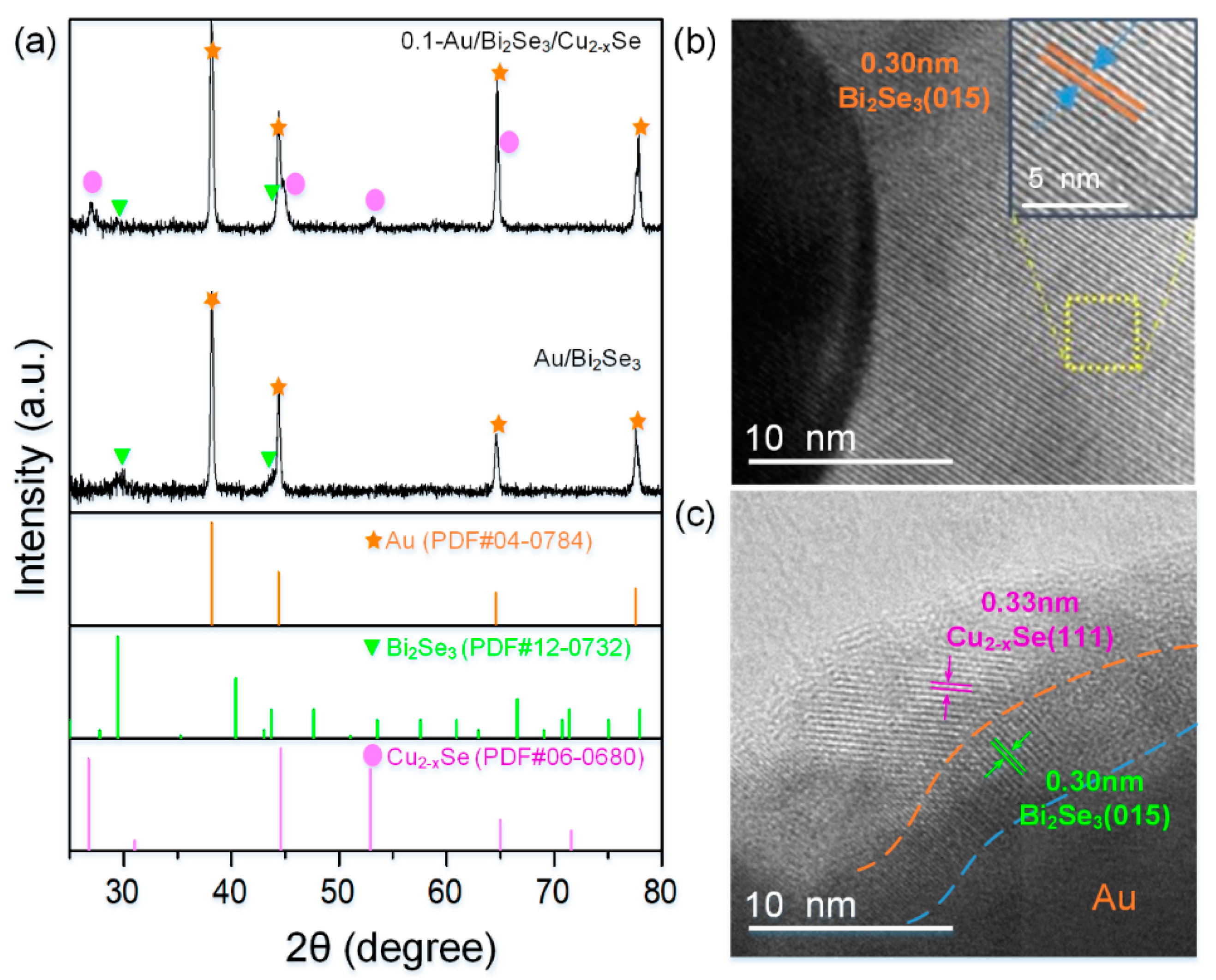
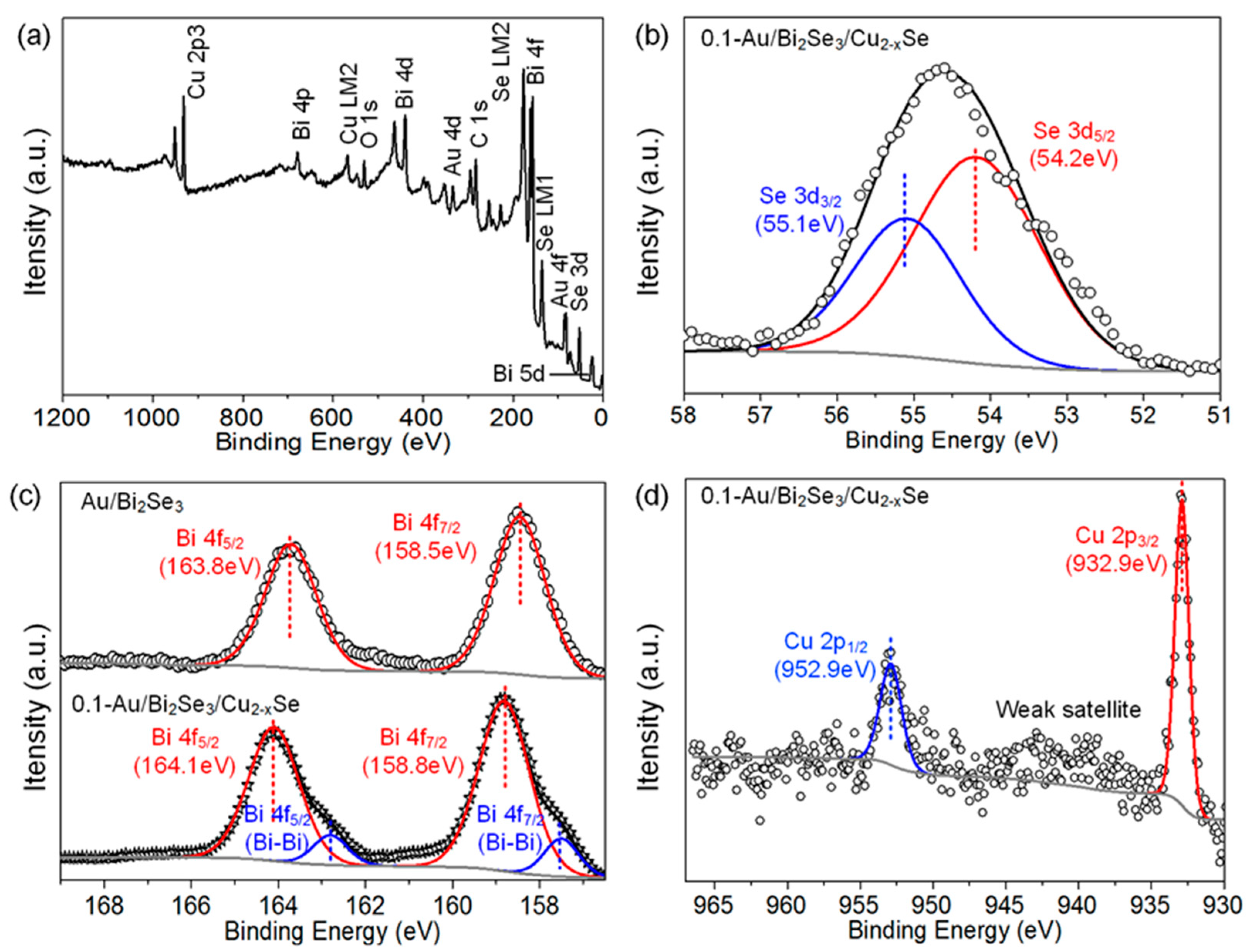
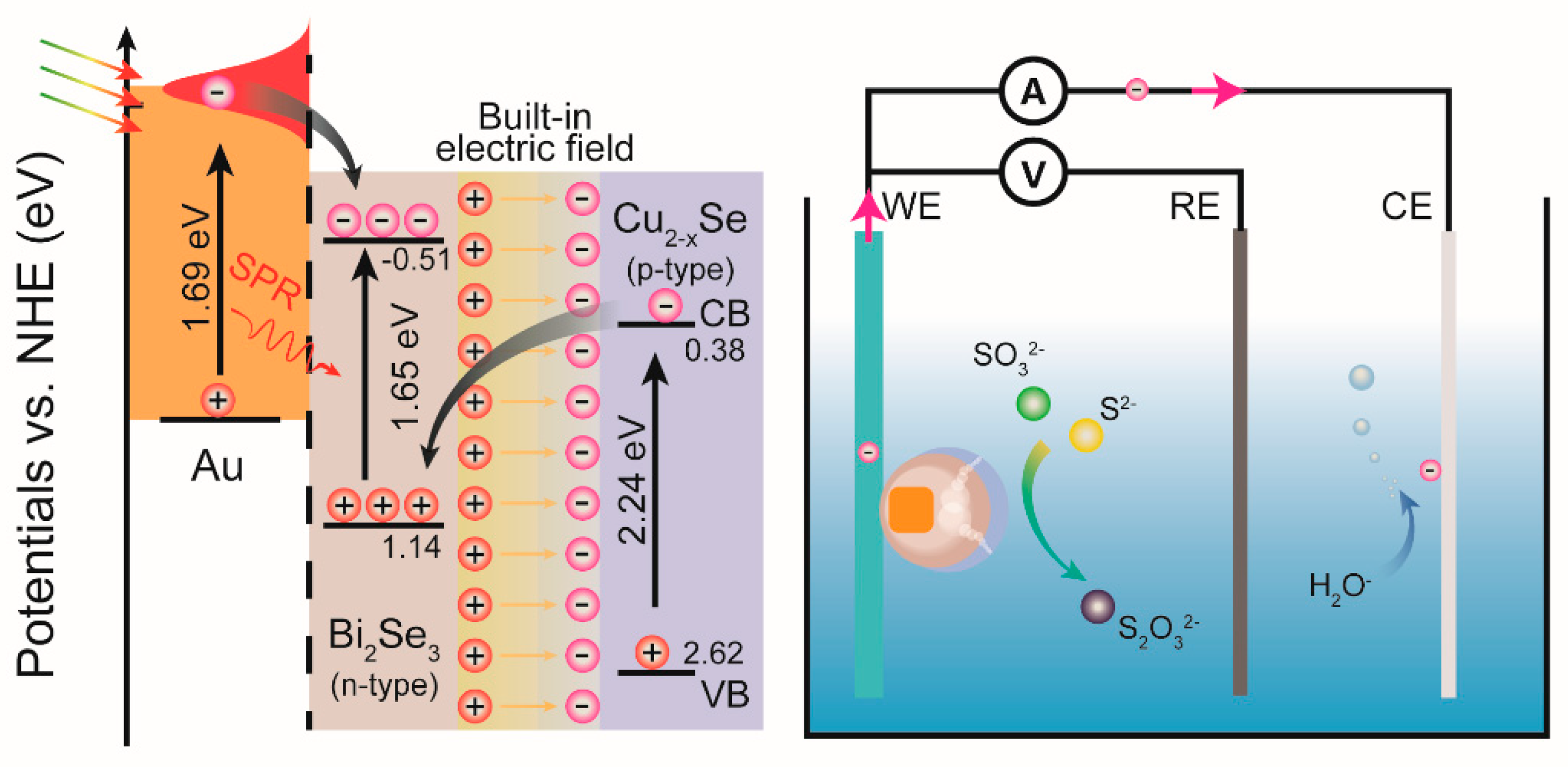
2. Results and Discussion

In this work, employed Au nanocubes (NCs) as the seeds, the porous Au/Bi2Se3/Cu2−xSe nanoparticles were fabricated through a simple three-step method, as illustrated in Figure 1a. Step one is the synthesis of the Au/Se Janus-like nanostructures. Using hexadecyltrimethylammonium bromide (CTAB) as the stabilizer, the Au seeds are coated with an amorphous Se layer by reducing SeO2 with the ascorbic acid (AA), forming Janus-shape Au/Se nanostructures. Step two is the preparation of porous Au/Bi2Se3 hybrid nanostructures with the help of glycine transporter. The detailed mechanism has been discussed in our previous work [21]. Last step is the formation of Bi2Se3/Cu2−xSe heterojunction. Cu2+ can be reduced to Cu+ by reducing agent AA, and then cation exchange reaction with Bi3+ ions in Au-Bi2Se3 solution can be performed to produce Cu2−xSe wetting layer on Au/Bi2Se3. Additionally, the epitaxial growth of Cu2−xSe shells inevitably occurs due to the presence of excess Se. The amount of Cu2−xSe can be further regulated by the initial Cu2+ precursor concentration (in Figure S1). Here, Cu2+ precursor concentration is set as x (x = 0.01 M, 0.1 M, and 0.4 M), and the obtained final product is labeled as x-Au/Bi2Se3/Cu2−xSe. Taking 0.1-Au/Bi2Se3/Cu2−xSe as an example, the corresponding synthesis process are characterized with the transmission electron microscopy (TEM) images in Figure 1b–e. The initial Au NCs synthesized by a seed-mediated method exhibit regular cube shape have an edge length of about 45 nm. Figure 1c clearly confirms forming Au/Se Janus-like nanostructure, the obtained Se layer is ~26 nm. As for the as-synthesized Au/Bi2Se3 nanoparticles in Figure 1d, the average thicknesses of corresponding semiconductor shells are ~27 nm, and some irregular pores are distributed in them. After the overgrowth of Cu2−xSe shells, the semiconductor shell’s thickness of Au/Bi2Se3/Cu2−xSe nanoparticle increases to 36 nm. As we can see in Figure 1e, many semiconductor nanocrystals are attached onto the surface of hybrid nanoparticle, suggesting the formation of Cu2−xSe nanocrystals on Bi2Se3 nanoshell.
The evolution of species and crystal structural for the products obtained at different reaction stages is monitored with corresponding X-ray diffraction (XRD) spectra and high-resolution TEM (HRTEM) images. As shown in Figure 2a, XRD measurement can be used to identify the lattice planes and crystal structure of synthesized Au/Bi2Se3 and Au/Bi2Se3/Cu2−xSe. The data reveal that all the samples have Au phase, and four diffraction peaks at 38.18°, 44.39°, 64.57° and 77.54° are ascribed to (111), (200), (220) and (311) planes of cubic Au according to joint committee on powder diffraction standards (JCPDS) cards no. 04-0784. As for Au/Bi2Se3 nanoparticles, in addition to diffraction peaks of Au phases, two diffraction peaks at 29.45° and 43.69° belong to (015) and (110) planes of rhombohedral Bi2Se3 (JCPDS card no. 12-0732). The sample Au/Bi2Se3/Cu2−xSe has three phases of Au, Bi2Se3 and Cu2−xSe, owing to the formation of Cu2−xSe nanocrystals. Besides the diffraction peaks of Au and Bi2Se3, four distinctive diffraction peaks appeared at 26.75°, 44.60°, 52.91° and 64.98° can be attributed to (111), (220), (311) and (400) planes of cubic Cu2−xSe (JCPDS card no. 06-0680), respectively. In Figure 2b,c, the representative HRTEM images of individual hybrid nanoparticles are further employed to reveal the overgrowth of Cu2−xSe on Au/Bi2Se3 nanoparticles. As we can see, two regions with different contrast can be clearly observed because of the different electron densities of metals and semiconductors, corresponding to Au core and semiconductor shell, respectively. Figure 2b shows the HRTEM image of individual Au/Bi2Se3 nanoparticle at its interface between metal and semiconductor, and the corresponding micro-area EDS result shown in Figure S2 suggests the presence of Au, Bi and Se elements. Uniform lattice fringe distribution is observed in the shell region, the lattice plane spacing of 0.30 nm can be referred to as the (015) lattice planes of rhombohedral Bi2Se3. The HRTEM image at the heterojunction of individual Au/Bi2Se3/Cu2−xSe nanoparticle is displayed in Figure 2c. The lattice spacing of 0.30 nm and 0.33 nm can be indexed as the (015) crystal plane of rhombohedral Bi2Se3 and the (111) crystal plane of cubic Cu2−xSe, respectively. All the results further confirm the overgrowth of Cu2−xSe on Au/Bi2Se3 nanoparticle.
In addition, X-ray photoelectron spectroscopy (XPS) was carried out to analyze the chemical composition and binding states of the sample. Figure 3a shows XPS survey spectrum of the sample Au/Bi2Se3/Cu2−xSe nanoparticles and Au, Se, Bi and Cu can be clearly observed. The corresponding high resolution XPS spectra of Se 3d, Cu 2p and Bi 4p are presented in Figure 3b–d. All XPS peaks were calibrated by C 1s peak at 284.8 eV. As we can see, the Se 3d spectrum in Figure 3b is deconvoluted into a doublet in a 3:2 area ratio, two XPS peaks appeared at 54.2 eV and 55.1 eV are assigned to Se 3d5/2 and Se 3d3/2, respectively, indicating the presence of Se2− species. In Figure 3c, the binding energies at 158.5 eV and 163.8 eV with a splitting of 5.3 eV are ascribed to Bi 4f7/2 and Bi 4f5/2 peaks of Bi2Se3 shells, respectively, which are in agreement with the reported values [45]. The two peaks located at 932.9 eV and 952.9 eV are ascribed to Cu 2p3/2 and Cu 2p1/2, respectively. A weak satellite peak around 942.5 eV lies between these two peaks, indicating the main valence sate of cooper element is Cu+ [26]. The intensity of corresponding XPS peaks enhances with the increasing of Cu2+ concentration in Figure S3, suggesting an increase of Cu2−xSe content. The results are consistent with TEM characterizations in Figure S1. In addition, a slightly positive shift (0.3 eV) of Bi 4f7/2 and Bi 4f5/2 in the Au/Bi2Se3/Cu2−xSe can be observed in Figure 3c. The positive shift of Bi 4f indicates a decrease of the electron density near the Bi element caused by electrons transfer at the interface, forming an internal electric field directing from Bi2Se3 to Cu2−xSe.
Figure 4a shows the evolution of absorption spectra of the samples in the different experimental stages. The absorption spectra of plasmonic metal nanocrystals are often strongly correlated to their morphologies and surrounding environments. The original Au NCs displays a strong resonance absorption band centered at 531 nm due to its surface plasmon resonance (SPR) behavior. After the formation of Janus-like Au/Se hetero nanostructures, the corresponding SPR peak shifts to 632 nm, attributing to the high refractive index of the amorphous Se shells. Subsequently, the SPR band of Au/Bi2Se3 hybrids further present an about 51 nm red shift. Meanwhile, a new absorption shoulder appears in the region of 420 to 450 nm, which can be ascribed to the formation of Bi2Se3 shells [46]. With the overgrowth of Cu2−xSe on Au/Bi2Se3 hybrids, the resonance absorption band of the sample appears red shift and broaden, which may be attributed to the effective coupling between Au core and semiconductor shells. In addition, the influence of initial Cu2+ precursor concentration on the absorption spectra of Au/Bi2Se3/Cu2−xSe hybrids was also presented in Figure 4b. All the obtained samples show the SPR peak centered at about 733 nm. As Cu2+ concentration increases from 0.05 M to 0.1 M, the corresponding resonance absorption peak becomes stronger and wider. Such a wide and strong spectral resonance absorption band matches well with the solar spectrum, allowing for their potential solar applications.
To evaluate the PEC water splitting performance of the obtained Au/Bi2Se3/Cu2−xSe hybrids, pure Bi2Se3, Au/Bi2Se3 and Au/Bi2Se3/Cu2−xSe NPs are loaded onto FTO working electrodes in a standard three-electrode electrochemical system, respectively. For comparison purposes, all samples have the same mass of corresponding components. Typical linear sweep voltammograms curves for five parallel electrodes are shown in Figure 5a. Under the simulated solar light, the photocurrent densities of the samples increase with the increase in applied potential. The photocurrent density of Au/Bi2Se3 electrode is 0.138 mA/cm2 at the applied potential of 1.20 V vs. the reversible hydrogen electrode (RHE), which is 1.58 times that of pure Bi2Se3 electrode (0.089 mA/cm2 at 1.20 V vs. RHE). Impressively, the photocurrent densities of 0.1-Au/Bi2Se3/Cu2−xSe, 0.4-Au/Bi2Se3/Cu2−xSe and 0.8-Au/Bi2Se3/Cu2−xSe electrodes are 0.375, 0.706 and 0.237 mA/cm2 at the applied potential of 1.20 V vs. RHE, respectively. 0.1-Au/Bi2Se3/Cu2−xSe photoanode presents the highest photocurrent density among the surveyed samples, which implies efficient photoelectron generation and interface transfer processes. In an illuminated three-electrode cell, the obtained current–voltage data can be useful to assess the solar conversion efficiency of photoelectrodes, which allows us to optimize and identify the champion nanostructure for high performance photoelectrochemical water splitting. The photoconversion efficiency (η) of samples can be calculated by using the following equation:
η = I (1.23 − U)/Jlight
where I is the photocurrent density (mA/cm2), U is the applied potential vs. RHE and Jlight is the irradiance intensity of incident light (100 mW/cm2). In Figure 5b, the maximum photoconversion efficiency of the samples increases in the order of Bi2Se3, Au/Bi2Se3 and x-Au/Bi2Se3/Cu2−xSe electrodes. A significant enhancement of photoconversion efficiency can be observed for Au/Bi2Se3 electrode by the introduction of Au NPs, owing to the plasmon-enhanced light harvesting. With the increasing of x, the maximum photoconversion efficiency of x-Au/Bi2Se3/Cu2−xSe electrode first increases and then decreases. 0.1-Au/Bi2Se3/Cu2−xSe electrode shows the optimal value of 0.11% at 0.95 V vs. RHE, which is 6.87 and 5.50 times that of Bi2Se3 (0.016% at 0.90 V vs. RHE) and Au/Bi2Se3 (0.02% at 0.90 V vs. RHE), demonstrating an excellent PEC water splitting performance.
To understand the enhanced mechanism of photocurrent response, photocurrent tests of the as-prepared Bi2Se3, Au/Bi2Se3 and x-Au/Bi2Se3/Cu2−xSe electrodes were performed at an applied potential of 1.23 V vs. RHE, respectively. As shown in Figure 6a, it shows the I-t curves for three parallel electrodes under white-light (AM 1.5 G, 100 mW/cm2). The photocurrents of all electrodes present a transient increase after illumination and a clear photo-switching behavior. The stable photocurrents of 0.122 and 0.181 mA/cm2 were correspondingly obtained for Bi2Se3 and Au/Bi2Se3 electrodes. By contrast, all x-Au/Bi2Se3/Cu2−xSe electrodes exhibit a significant photocurrent enhancement. More notably, the photocurrent density of 0.1-Au/Bi2Se3/Cu2−xSe electrode is 0.741 mA/cm2. Compared with Bi2Se3 and Au/Bi2Se3 electrodes, 0.1-Au/Bi2Se3/Cu2−xSe electrode presents 5.07 and 3.09 times of photoresponse enhancement, respectively. Combined with absorption spectrum in Figure 4a, the observed photoresponse enhancement may be attributed to plasmon-induced absorption enhancement and hot-electron injection. However, when x increases from 0.05 to 0.4, the photocurrent response of x-Au/Bi2Se3/Cu2−xSe electrodes do not continue to increase with the light absorption enhancement but increases first and then decreases. The results indicate that there is another mechanism to improve the photoelectrochemical properties of the samples besides the enhanced light absorption. During the testing process, time-dependent photocurrent, XRD spectra and corresponding photo images of the sample are further recorded in Figure S4. The data show that the photocurrent density and crystal structure of the Au/Bi2Se3/Cu2−xSe electrode remains almost unchanged, indicating the structural stability for potential applications. Subsequently, electrochemical impedance spectroscopy (EIS) experiments were carried out at open circuit potential under white light illumination to get further insight into the charge transfer and recombination processes. As shown in Figure 6b, Rs denotes the contact resistances of the electrochemical device, CPE denotes the capacitance phase element, Rct denotes the interfacial charge transfer resistance and the arc radius on Nyquist plot is primarily proportional to the charge transfer resistance Rct. The values of Rct are calculated to be 1229, 668 and 432 Ω for pure Bi2Se3, Au/Bi2Se3 and 0.1-Au/Bi2Se3/Cu2−xSe electrodes, respectively. Au/Bi2Se3/Cu2−xSe electrode shows the lowest arc radius, indicating a lower charge transfer resistance. These results can be attributed to the formation of Au/Bi2Se3 and Bi2Se3/Cu2−xSe multi-interface heterojunctions improving charge carries separation and transfer. The electron lifetime ( τ n ) is related to the characteristic frequency peaks f m a x in Bode phase plots diagrams, that is τ n = 1 / 2 π f m a x [47]. As shown in Figure 6c, the characteristic peak values for pure Bi2Se3, Au/Bi2Se3 and Au/Bi2Se3/Cu2−xSe electrodes (below 100 Hz) are 96.42, 37.76 and 1.89 Hz, respectively. The corresponding τ n values are 1.65, 4.21 and 86.03 ms in turn. Besides that, we further compare the photoelectron transport performance in interfaces of x-Au/Bi2Se3/Cu2−xSe electrodes. As shown in Figure 6d, the radius of arch in the impedance spectra appears decrease first and then increase along with the x value increasing. The data indicates that the right-sized Cu2−xSe in Au/Bi2Se3/Cu2−xSe is non-negligible to their photoelectrochemical properties. The corresponding characteristic frequency peak values in Bode phase plots are 1.85 Hz, 2.73 Hz and 4.44 Hz for 0.05, 0.1 and 0.4-Au/Bi2Se3/Cu2−xSe electrodes, respectively. The electrons lifetime in 0.1-Au/Bi2Se3/Cu2−xSe electrode is the longest among them, which means the FTO substrate possesses more opportunities to collect electrons produced by the electrode. As thus, all the results suggest that Au/Bi2Se3/Cu2−xSe can effectively inhibit the charge recombination for superior solar-driven water splitting performance.
In addition, the Mott–Schottky diagrams and absorption spectra of pure Bi2Se3 and Cu2−xSe NPs prepared at the same conditions are displayed in Figure S5. The pure Bi2Se3 and Cu2−xSe are presented with a positive and negative slope in the Mott–Schottky diagrams, implying that Bi2Se3 is a p-type semiconductor and Cu2−xSe is an n-type semiconductor. From the x-intercepts of linear extrapolations, the flat-band potentials of Bi2Se3 and Cu2−xSe can be determined to be −0.21 V vs. RHE and 2.32 V vs. RHE, respectively. Their band gap energies (Eg) can be estimated as 1.65 and 2.24 eV from the Tauc plots (in Figure S4), respectively. Based on the above results, the direct Z-scheme migration pathway of the photogenerated carriers for Au/Bi2Se3/Cu2−xSe electrode can be depicted in Figure 7. Here, when p-type Cu2−xSe encounters with n-type Bi2Se3, electrons on the Bi2Se3 will migrate to Cu2−xSe to obtain a Fermi level equilibrium, leaving an internal electric field from Bi2Se3 to Cu2−xSe at the interface. Upon light irradiation, photoelectrons at the interface will be driven into the Bi2Se3 by the internal electric field, accelerating the charge carrier separation according to the direct Z-scheme mechanism. Considering the Fermi level of Au and the Schottky barrier (≈0.9 eV) at the Au-Bi2Se3 interface, the plasmon-induced hot electrons (1.69 eV) in Au core have sufficient energy to surmount the Schottky barrier and injected into the conduction band of Bi2Se3 shell. Simultaneously, the SPR band of Au/Bi2Se3/Cu2−xSe hybrids lies in the same spectral region as the Bi2Se3 absorption edge, which will induce a resonance coupling between Au with Bi2Se3 and effectively promote the harvesting of visible light of the photoelectrode. Furthermore, the hollow and porous nanoshells not only maintain the independence of the plasmon nanostructures, but also provide a channel for the connection between the Au core and the solution. Therefore, hot holes can be rapidly eliminated by the hole scavengers to recycle the photoreduction/oxidation reactions.

3. Materials and Methods

3.1. Chemicals and Materials

Chloroauric acid (HAuCl4·H2O, 99.99%), hexadecyltrimethylammonium bromide (CTAB, 99%), sodium borohydride (NaBH4,96%), L-ascorbic acid (AA, 99.7%), glycine acid (Gly, 99.5), selenium dioxide (SeO2, 99%), bismuth (III) nitrate pentahydrate (Bi(NO3)3·5H2O), copper(II) sulfate pentahydrate (CuSO4·5H2O, 99%), sodium sulfite anhydrous (Na2SO3, 97%), sodium sulfide nonahydrate (Na2S·9H2O, 98%) was purchased from Sinopharm Chemical Reagent Co. Ltd. (Shanghai, China). All chemicals were used as received and without further purification. All aqueous solutions were freshly prepared in the water obtained by ultra-pure water system from ZOOMWO Co. Ltd. (Hunan, China).

3.2. Synthesis of the Au Nanocubes

Au NCs were prepared by using a seed-mediated growth method [48]. The seed solution for Au NCs growth was prepared as follows: 0.25 mL of chloroauric acid (5.0 mM) and 3.75 mL of CTAB (0.1 M) was added into a vial at room temperature. One-hundred-and-fifty microliters of fresh-prepare and ice-cold NaBH4 (0.01 M) was rapidly injected with vigorous stirring. Subsequently, the mixture was kept on gently stirring for 1 h. To prepare the growth solution, 12.8 mL of CTAB (0.1 M) and 1.6 mL of HAuCl4 (0.01 M) were added into a 100 mL round-bottom flask with 62.4 mL deionized water. After then, 7.6 mL of ascorbic acid (0.1 M) was injected to the flask with gentle mixing. The color of the mixed solution changed from gold to colorless. Finally, 40 μL of 10 times diluted Au seed solution was added to the round-bottom flask and mix it gently for 30 s. The solution was allowed to stand in the flask overnight at 37 °C without stirring.

3.3. Synthesis of Porous Au/Bi2Se3 Nanoparticles

First, 60 mL of CTAB-stabilized Au nanocubes was centrifuged at 8000 rpm for 10 min to synthesize Au/Se intermediates. Second, the supernatant was removed, and the obtained precipitate was redispersed into a test tube with 20 mL of CTAB (0.2 M). Then, 0.2 mL of SeO2 (0.1 M) and 1 mL of AA (0.1 M) were added successively. The solution was stirred for 5 h at 40 °C water bath. To prepared porous Au/Bi2Se3 nanoparticles, the mixture was transferred to 60 °C oil bath subsequently. Twenty milliliters of glycine (0.2 M), 1 mL of AA (0.1M) and 1.6 mL of Bi (NO3)3 (0.01 M, dissolved by 0.35 M HNO3) were rapidly injected to the reaction solution. The mixed solution was kept at 80 °C under vigorously stirring for 5 h. The final products were washed by deionized water and collected by centrifugation at 8000 rpm for 10 min.

3.4. Synthesis of the Porous Au/Bi2Se3/Cu2−xSe Nanoparticles

The obtained Au/Bi2Se3 nanoparticles were dispersed into the mixed solvents of 40 mL of CTAB (0.1 M) and 20 mL glycine (0.2 M). Next, a freshly prepared mixture of CuSO4 (0.1 M) and AA (0.1 M) aqueous solution (the volume ratio of CuSO4/AA was 1:4) was added under vigorous stirring. The mixture was allowed to react under vigorous stirring at 60 °C for 90 min. The obtained products were centrifuged at 8000 rpm for 9 min, and then redispersed in ultra-pure water for further use.

3.5. Photoelectrochemical (PEC) Tests

The PEC measurements were performed using a standard three-electrode potentiostat system on Instruments CS350 electrochemical workstation (Corrtest, Wuhan, China) with a working electrode, Pt counterelectrode and Ag/AgCl reference electrode. FTO substrate (1 cm × 2 cm) was first cleaned with ethanol and then water. In order to enhance the photoelectron collecting ability and stability of the electrode, the surface of FTO was modified by conductive silver adhesives. Then, the working electrode was prepared by depositing active films of the sample on the modified FTO substrate. The surface area of the sample exposed to the electrolyte was fixed at 1 cm2. An aqueous solution containing 0.2 M of Na2S and 0.2 M of Na2SO3 (pH ≈ 12.4) was used as the electrolyte to maintain the stability of the electrodes. Linear Sweep Voltammetry (LSV) curves had a scan rate of 10 mV s−1. Chronoamperometry was applied at the potential of 1.23 V vs. RHE. Electrochemical impedance spectroscopy (EIS) was measured under open circuit conditions (AC amplitude).

3.6. Morphology and Structure Characterizations

TEM and HRTEM observations were performed with a FEI Tecnai F20 transmission electron microscope operated at 200 kV (FEI Company, Hillsboro, OR, USA) The XRD analyses were performed on a Bruker D8-advance X-ray diffractometer (Bruker AXS, Billerica, Germany) with Cu kαirradiation (λ = 1.5406 Å). Absorption spectra of the samples were measured using a TU-1810 UV-Vis’s spectrophotometer (Purkinje General Instrument Co. Ltd., Beijing, China). XPS (Thermo Fisher Scientific, USA) was recorded by a Thermo Fisher Scientific Esca lab 250Xi X-ray photoelectron spectrometer with a monochromatic Al Ka irradiation.

4. Conclusions

In summary, we have prepared Cu2−xSe decorated Au/Bi2Se3 porous nanoparticles by a simple three-step method. Bi2Se3/Cu2−xSe z-scheme heterojunction was introduced onto Au nanocube through a cation exchange method. The obtained Au/Bi2Se3/Cu2−xSe hybrids possessed a broad and strong plasmon resonance absorption in the visible bands, owing to the effective coupling between Au core and semiconductor nanoshells. More intriguingly, the carrier lifetime of Au/Bi2Se3/Cu2−xSe hybrid photoelectrodes could be further tailored with corresponding Cu2−xSe content. Through parameter optimization, 0.1-Au/Bi2Se3/Cu2−xSe hybrid photoanodes exhibited the longest electron lifetime (86.03 ms) among all the survey samples and demonstrated a decent photoelectrochemical performance enhancement in the tests. Compared with the pure Bi2Se3 (0.016% at 0.90 V vs. RHE) and Au/Bi2Se3 (0.02% at 0.90 V vs. RHE) nanoparticles photoanodes, the maximum photoconversion efficiency of porous Au/Bi2Se3/Cu2−xSe hybrid photoanodes increased by 5.87 and 4.50 times under simulated sunlight illumination, all the results could be attributed to the synergistic effect of Z-scheme heterojunction and plasmon resonance enhancement. All the results suggest that Au/Bi2Se3/Cu2−xSe porous nanostructures combine eco-friendliness with excellent sunlight harvesting capability and effectively inhibiting the charge recombination, which provide a new opportunity for efficient solar-driven water splitting.

Supplementary Materials

The following supporting information can be downloaded at: https://www.mdpi.com/article/10.3390/catal12040359/s1, Refs [49,50], Figure S1: TEM images of the obtained Au/Bi2Se3/Cu2−xSe porous hybrid nanostructures with initial Cu2+ precursor concentration of (a) 0.05 M, (b) 0.1 M and (c) 0.4 M; Figure S2: The EDS spectrum of Au/Bi2Se3 hybrid nanoparticle recorded at the area shown in Figure 2b; Figure S3: Cu 2p XPS spectra of Au/Bi2Se3/Cu2−xSe porous hybrid nanostructures with initial Cu2+ precursor concentration of 0.05 M, 0.1 M and 0.4 M.; Figure S4: (a) The time-dependent photocurrent, (b) XRD spectra and corresponding photo images of the sample are recorded during the testing process; Figure S5: (a) Absorption spectra and (b) corresponding (αhν)2 versus hν curves of pure Bi2Se3 and Cu2−xSe nanocrystals. Mott–Schottky diagrams tested at an AC frequency of 1 kHz in the dark for pure (c) Bi2Se3 and (d) Cu2−xSe nanocrystals; Approximate band structure analysis.

Author Contributions

The manuscript was written through contributions of all authors. Conceptualization, S.L. and L.Z.; methodology and investigation, L.H., W.C. and X.L.; visualization, L.H. and Y.L.; data curation, L.H. and S.L.; writing—original draft preparation, S.L., J.L. and L.Z.; writing—review and editing, S.L., Z.C. and L.Z. All authors have read and agreed to the published version of the manuscript.

Funding

This research was funded by the Natural Science Foundation of Hunan Province (Grant Nos. 2019JJ50367, 2020JJ4935) and undergraduate Student Innovation Experiment Project of Hunan normal university (Grant No. 2019132).

Data Availability Statement

The data are available upon request from the corresponding author.

Acknowledgments

The authors thank M. Jiang, Y. Yin and X. Zhong (school of physics and electronics, Hunan Normal University, Changsha 410081, China) for their help.

Conflicts of Interest

The authors declare no conflict of interest.

References

  1. Dresselhaus, M.S.; Thomas, I.L. Alternative energy technologies. Nature 2001, 414, 332–337. [Google Scholar] [CrossRef] [PubMed]
  2. Chu, S.; Majumdar, A. Opportunities and challenges for a sustainable energy future. Nature 2012, 488, 294–303. [Google Scholar] [CrossRef] [PubMed]
  3. Yamaguchi, Y.; Kudo, A. Visible light responsive photocatalysts developed by substitution with metal cations aiming at artificial photosynthesis. Front. Energy 2021, 15, 568–576. [Google Scholar] [CrossRef]
  4. Tasleem, S.; Tahir, M. Recent progress in structural development and band engineering of perovskites materials for photocatalytic solar hydrogen production: A review. Int. J. Hydrogen Energy 2020, 45, 19078–19111. [Google Scholar] [CrossRef]
  5. Hong, J.; Xu, C.; Deng, B.; Gao, Y.; Zhu, X.; Zhang, X.; Zhang, Y. Photothermal chemistry based on solar energy: From Synergistic Effects to Practical Applications. Adv. Sci. 2021, 9, e2103926. [Google Scholar] [CrossRef] [PubMed]
  6. Gaya, U.I.; Abdullah, A.H. Heterogeneous photocatalytic degradation of organic contaminants over titanium dioxide: A review of fundamentals, progress and problems. J. Photochem. Photobiol. C 2008, 9, 1–12. [Google Scholar] [CrossRef]
  7. Chen, S.; Huang, D.; Xu, P.; Xue, W.; Lei, L.; Cheng, M.; Wang, R.; Liu, X.; Deng, R. Semiconductor-based photocatalysts for photocatalytic and photoelectrochemical water splitting: Will we stop with photocorrosion. J. Mater. Chem. A 2020, 8, 2286–2322. [Google Scholar] [CrossRef]
  8. Yao, T.; An, X.; Han, H.; Chen, J.Q.; Li, C. Photoelectrocatalytic materials for solar water splitting. Adv. Energy Mater. 2018, 8, 1800210. [Google Scholar] [CrossRef]
  9. Tournet, J.; Lee, Y.; Karuturi, S.K.; Tan, H.H.; Jagadish, C. III–V semiconductor materials for solar hydrogen production: Status and prospects. ACS Energy Lett. 2020, 5, 611–622. [Google Scholar] [CrossRef]
  10. Niu, F.; Wang, D.; Li, F.; Liu, Y.; Shen, S.; Meyer, T.J. Hybrid photoelectrochemical water splitting systems: From interface design to system assembly. Adv. Energy Mater. 2019, 10, 1900399. [Google Scholar] [CrossRef]
  11. Fujishima, A.; Honda, K. Electrochemical photolysis of water at a semiconductor electrode. Nature 1972, 238, 37–38. [Google Scholar] [CrossRef] [PubMed]
  12. Zeng, C.; Dai, L.; Jin, Y.; Liu, J.; Zhang, Q.; Wang, H. Design strategies toward transition metal selenide-based catalysts for electrochemical water splitting. Sustain. Energy Fuels 2021, 5, 1347–1365. [Google Scholar] [CrossRef]
  13. Wang, M.; Wang, S.; Zhang, Q.; Pan, S.; Zhao, Y.; Zhang, X. Controlling the crystallographic orientation of Sb2Se3 film for efficient photoelectrochemical water splitting. Sol. RRL 2021, 2100798. [Google Scholar] [CrossRef]
  14. Wang, H.; Xia, Y.; Wen, N.; Shu, Z.; Jiao, X.; Chen, D. Surface states regulation of sulfide-based photoanode for photoelectrochemical water splitting. Appl. Catal. B-Environ. 2022, 300, 120717. [Google Scholar] [CrossRef]
  15. Chandrasekaran, S.; Yao, L.; Deng, L.; Bowen, C.; Zhang, Y.; Chen, S.; Lin, Z.; Peng, F.; Zhang, P. Recent advances in metal sulfides: From controlled fabrication to electrocatalytic, photocatalytic and photoelectrochemical water splitting and beyond. Chem. Soc. Rev. 2019, 48, 4178–4280. [Google Scholar] [CrossRef]
  16. Xiao, L.; Liu, Q.; Zhang, M.; Liu, L. Photoelectric properties of Bi2Se3 films grown by thermal evaporation method. Mater. Res. Express 2020, 7, 016429. [Google Scholar] [CrossRef]
  17. Liao, G.; Zhou, Y.; Huang, Z.; Ma, Q.; Luo, S.; Liu, Y.; Qi, X. Bi2Se3 nanosheets hybridized with reduced graphene oxide for enhanced photoelectrochemical activity. Appl. Phys. A 2021, 127, 705. [Google Scholar] [CrossRef]
  18. Li, M.; Zhang, Y.; Zhang, T.; Zuo, Y.; Xiao, K.; Arbiol, J.; Llorca, J.; Liu, Y.; Cabot, A. Enhanced thermoelectric performance of n-type Bi2Se3 nanosheets through Sn doping. Nanomaterials 2021, 11, 1827. [Google Scholar] [CrossRef] [PubMed]
  19. Li, D.; Fang, M.; Jiang, C.; Lin, H.; Luo, C.; Qi, R.; Huang, R.; Peng, H. Size-controlled synthesis of hierarchical bismuth selenide nanoflowers and their photocatalytic performance in the presence of H2O2. J. Nanopart. Res. 2018, 20, 228. [Google Scholar] [CrossRef]
  20. Wang, C.C.; Shieu, F.S.; Shih, H.C. Photosensing and characterizing of the pristine and In-, Sn-Doped Bi2Se3 nanoplatelets fabricated by thermal V-S Process. Nanomaterials 2021, 11, 1352. [Google Scholar] [CrossRef]
  21. Tang, L.; Liang, S.; Li, J.B.; Zhang, D.; Chen, W.B.; Yang, Z.J.; Xiao, S.; Wang, Q.Q. Controlled synthesis of Au nanocrystals-metal selenide hybrid nanostructures toward plasmon-enhanced photoelectrochemical energy conversion. Nanomaterials 2020, 10, 564. [Google Scholar] [CrossRef] [PubMed] [Green Version]
  22. Liu, X.-D.; Chen, B.; Wang, G.-G.; Ma, S.; Cheng, L.; Liu, W.; Zhou, L.; Wang, Q.-Q. Controlled growth of hierarchical Bi2Se3/CdSe-Au nanorods with optimized photothermal conversion and demonstrations in photothermal therapy. Adv. Funct. Mater. 2021, 31, 2104424. [Google Scholar] [CrossRef]
  23. Liu, D.; Chen, S.; Li, R.; Peng, T. Review of Z-scheme heterojunctions for photocatalytic energy conversion. Acta Phys.-Chim. Sin. 2020, 37, 2010017. [Google Scholar] [CrossRef]
  24. Kudo, A.; Miseki, Y. Heterogeneous photocatalyst materials for water splitting. Chem. Soc. Rev. 2009, 38, 253–278. [Google Scholar] [CrossRef]
  25. Wang, Y.; Shuai, X.; Zhang, J.; Zhao, R.; Guo, T.; Du, J.; Zheng, J.; Li, J. Engineering of band structure of bismuth selenide ultrathin nanosheets as multifunctional material for photocatalytic application. Adv. Mater. Interfaces 2022, 2102417. [Google Scholar] [CrossRef]
  26. Liu, Y.; Shen, S.; Zhang, J.; Zhong, W.; Huang, X. Cu2−xSe/CdS composite photocatalyst with enhanced visible light photocatalysis activity. Appl. Surf. Sci. 2019, 478, 762–769. [Google Scholar] [CrossRef]
  27. Marbella, L.E.; Gan, X.Y.; Kaseman, D.C.; Millstone, J.E. Correlating carrier density and emergent plasmonic features in Cu2−xSe nanoparticles. Nano Lett. 2017, 17, 2414–2419. [Google Scholar] [CrossRef]
  28. Xu, Q.; Zhang, L.; Cheng, B.; Fan, J.; Yu, J. S-scheme heterojunction photocatalyst. Chem 2020, 6, 1543–1559. [Google Scholar] [CrossRef]
  29. Wang, W.; Ma, S.; Chen, K.; Wang, P.-F.; Liu, Q.-Y.; Zhou, L.; Wang, Q.-Q. Controlled growth of Cu2−xS sheet-like nanoshells and Cu2−xS-CdS p-n junctions on Au nanorods with coupled plasmon resonances and enhanced photocatalytic activities. J. Mater. Chem. C 2020, 8, 3058–3068. [Google Scholar] [CrossRef]
  30. Thongam, D.D.; Chaturvedi, H. Advances in nanomaterials for heterogeneous photocatalysis. Nano Express 2021, 2, 012005. [Google Scholar] [CrossRef]
  31. Ng, B.J.; Putri, L.K.; Kong, X.Y.; Teh, Y.W.; Pasbakhsh, P.; Chai, S.P. Z-scheme photocatalytic systems for solar water splitting. Adv. Sci. 2020, 7, 1903171. [Google Scholar] [CrossRef] [PubMed]
  32. Liu, Z.; Wang, L.; Yu, X.; Zhang, J.; Yang, R.; Zhang, X.; Ji, Y.; Wu, M.; Deng, L.; Li, L.; et al. Piezoelectric-effect-enhanced full-spectrum photoelectrocatalysis in p-n heterojunction. Adv. Funct. Mater. 2019, 29, 1807279. [Google Scholar] [CrossRef]
  33. Wu, Z.; Yuan, D.; Lin, S.; Guo, W.; Zhan, D.; Sun, L.; Lin, C. Enhanced photoelectrocatalytic activity of Bi2S3–TiO2 nanotube arrays hetero-structure under visible light irradiation. Int. J. Hydrogen Energy 2020, 45, 32012–32021. [Google Scholar] [CrossRef]
  34. Moniz, S.J.A.; Shevlin, S.A.; Martin, D.J.; Guo, Z.-X.; Tang, J. Visible-light driven heterojunction photocatalysts for water splitting—A critical review. Energy Environ. Sci. 2015, 8, 731–759. [Google Scholar] [CrossRef]
  35. Baviskar, V.S.; Salunkhe, D.B.; Patil, G.P.; Jadhav, C.D.; Nerkar, D.M.; Baviskar, P.K.; Patil, R.S. Effect of deposition time on photoelectrochemical performance of chemically grown Bi2Se3-sensitized TiO2 nanostructure solar cells. Acta Phys.-Chim. Sin. 2020, 31, 17440–17450. [Google Scholar] [CrossRef]
  36. Wang, Y.; Wang, W.; Sang, D.; Yu, K.; Lin, H.; Qu, F. Cu2−xSe/Bi2Se3@PEG Z-scheme heterostructure: A multimode bioimaging guided theranostic agent with enhanced photo/chemodynamic and photothermal therapy. Biomater. Sci. 2021, 9, 4473–4483. [Google Scholar] [CrossRef]
  37. Chen, S.; Ma, G.; Wang, Q.; Sun, S.; Hisatomi, T.; Higashi, T.; Wang, Z.; Nakabayashi, M.; Shibata, N.; Pan, Z.; et al. Metal selenide photocatalysts for visible-light-driven Z-scheme pure water splitting. J. Mater. Chem. A 2019, 7, 7415–7422. [Google Scholar] [CrossRef] [Green Version]
  38. Subramanyam, P.; Meena, B.; Suryakala, D.; Subrahmanyam, C. TiO2 photoanodes sensitized with Bi2Se3 nanoflowers for visible–near-infrared photoelectrochemical water splitting. ACS Appl. Nano Mater. 2021, 4, 739–745. [Google Scholar] [CrossRef]
  39. Zhuang, T.T.; Liu, Y.; Sun, M.; Jiang, S.L.; Zhang, M.W.; Wang, X.C.; Zhang, Q.; Jiang, J.; Yu, S.H. A unique ternary semiconductor-(semiconductor/metal) nano-architecture for efficient photocatalytic hydrogen evolution. Angew. Chem. Int. Ed. 2015, 54, 11495–11500. [Google Scholar] [CrossRef]
  40. Cai, X.; Chen, Q.; Wang, R.; Wang, A.; Wang, J.; Zhong, S.; Liu, Y.; Chen, J.; Bai, S. Integration of plasmonic metal and cocatalyst: An efficient strategy for boosting the visible and broad spectrum photocatalytic H2 evolution. Adv. Mater. Interfaces 2019, 6, 1900775. [Google Scholar] [CrossRef]
  41. Chen, K.; Gong, L.-L.; Ding, S.-J.; Liu, J.; Ma, S.; Wang, J.-H.; Yang, D.-J.; Pan, G.-M.; Hao, Z.-H.; Zhou, L.; et al. Tunable charge transfer and dual plasmon resonances of Au@WO3−x hybrids and applications in photocatalytic hydrogen generation. Plasmonics 2019, 15, 21–29. [Google Scholar] [CrossRef]
  42. Chen, W.-B.; Hu, L.-Y.; Meng, F.; Tang, L.; Liang, S.; Li, J.-B. Dual-plasmon-induced photocatalytic performance enhancement in Au-PbS-CdS nanodumbbells with double Au caps on the ends. Opt. Mater. 2021, 117, 111210. [Google Scholar] [CrossRef]
  43. Li, D.; Lao, J.; Jiang, C.; Luo, C.; Qi, R.; Lin, H.; Huang, R.; Waterhouse, G.I.N.; Peng, H. Plasmonic Au nanoparticle-decorated Bi2Se3 nanoflowers with outstanding electrocatalytic performance for hydrogen evolution. Int. J. Hydrogen Energy 2019, 44, 30876–30884. [Google Scholar] [CrossRef]
  44. Ma, S.; Chen, K.; Qiu, Y.-H.; Gong, L.-L.; Pan, G.-M.; Lin, Y.-J.; Hao, Z.-H.; Zhou, L.; Wang, Q.-Q. Controlled growth of CdS–Cu2-xS lateral heteroshells on Au nanoparticles with improved photocatalytic activity and photothermal efficiency. J. Mater. Chem. A 2019, 7, 3408–3414. [Google Scholar] [CrossRef]
  45. Li, D.; Lao, J.; Jiang, C.; Shen, Y.; Luo, C.; Qi, R.; Lin, H.; Huang, R.; Waterhouse, G.I.N.; Peng, H. Heterostructured MoS2@Bi2Se3 nanoflowers: A highly efficient electrocatalyst for hydrogen evolution. J. Catal. 2020, 381, 590–598. [Google Scholar] [CrossRef]
  46. Mohammadniaei, M.; Lee, T.; Bharate, B.G.; Yoon, J.; Choi, H.K.; Park, S.J.; Kim, J.; Kim, J.; Choi, J.W. Bifunctional Au@Bi2Se3 core−shell nanoparticle for synergetic therapy by SERS-Traceable AntagomiR delivery and photothermal treatment. Small 2018, 14, 1802934. [Google Scholar] [CrossRef]
  47. Pang, Y.; Zang, W.; Kou, Z.; Zhang, L.; Xu, G.; Lv, J.; Gao, X.; Pan, Z.; Wang, J.; Wu, Y. Assembling of Bi atoms on TiO2 nanorods boosts photoelectrochemical water splitting of semiconductors. Nanoscale 2020, 12, 4302–4308. [Google Scholar] [CrossRef]
  48. Liu, X.-L.; Liang, S.; Li, M.; Yu, X.-F.; Zhou, L.; Wang, Q.-Q. Facile synthesis of Au nanocube-CdS core-shell nanocomposites with enhanced photocatalytic activity. Chin. Phys. Lett. 2014, 31, 064203. [Google Scholar] [CrossRef]
  49. Bai, S.; Jiang, J.; Zhang, Q.; Xiong, Y. Steering charge kinetics in photocatalysis: Intersection of materials syntheses, characterization techniques and theoretical simulations. Chem. Soc. Rev. 2015, 44, 2893–2939. [Google Scholar] [CrossRef] [PubMed]
  50. Zhang, L.; Ran, J.; Qiao, S.Z.; Jaroniec, M. Characterization of semiconductor photocatalysts. Chem. Soc. Rev. 2019, 48, 5184–5206. [Google Scholar] [CrossRef]
Figure 1. (a) Schematic illustration of synthetic process for porous Au/Bi2Se3/Cu2−xSe hybrid nanoparticles by three-step strategy. TEM images of (b) Au nanocubes, (c) Au/Se, (d) Au/Bi2Se3, and (e) Au/Bi2Se3/Cu2−xSe hybrid nanoparticles.
Catalysts 12 00359 g001
Figure 2. (a) XRD spectra of Au/Bi2Se3 and Au/Bi2Se3/Cu2−xSe nanoparticles. Corresponding HRTEM images of individual (b) Au/Bi2Se3 and (c) Au/Bi2Se3/Cu2−xSe nanoparticles at their interfaces. The white arrows indicate the regions of nanopores.
Catalysts 12 00359 g002
Figure 3. (a) XPS survey spectrum of Au/Bi2Se3/Cu2−xSe nanoparticles and high-resolution XPS spectra of Au/Bi2Se3 and Au/Bi2Se3/Cu2−xSe hybrids at binding energies corresponding to (b) Bi 4f, (c) Se 3d (d) and Cu 2p, respectively.
Catalysts 12 00359 g003
Figure 4. (a) UV–Vis absorption spectra of as-synthesized Au NCs, Au/Se, Au/Bi2Se3 and Au/Bi2Se3/Cu2−xSe nanoparticles. (b) UV–Vis spectra of Au/Bi2Se3/Cu2−xSe nanoparticles with different amount of Cu2−xSe, and the added Cu2+ concentrations are 0.05, 0.1 and 0.4 M, respectively.
Catalysts 12 00359 g004
Figure 5. (a) Linear sweep voltammogram measurements and (b) calculated photoconversion efficiencies of Bi2Se3, Au/Bi2Se3 and x-Au/Bi2Se3/Cu2−xSe electrodes under the chopped sunlight illumination.
Catalysts 12 00359 g005
Figure 6. (a) Time-dependent photocurrent intensity, (b) Nyquist and (c) Bode phase plots for FTO photoanodes loaded with Bi2Se3, Au/Bi2Se3 and x-Au/Bi2Se3/Cu2−xSe at 1.23 V vs. RHE with white-light irradiation (AM 1.5 G, 100 mW/cm2). (d) Corresponding electrochemical impedance spectroscopy tests for four Au/Bi2Se3/Cu2−xSe photoanodes with different initial Cu2+ concentration.
Catalysts 12 00359 g006
Figure 7. Schematic illustration of device configuration and proposed energy band structure of FTO photoelectrode sensitized with Au/Bi2Se3/Cu2−xSe hybrids.
Catalysts 12 00359 g007
Publisher’s Note: MDPI stays neutral with regard to jurisdictional claims in published maps and institutional affiliations.

