Abstract
A Ring Oscillator Physical Unclonable Function (RO PUF) is an application-constrained hardware security primitive that can be used for authentication and key generation. PUFs depend on variability during the fabrication process to produce random outputs that are nevertheless stable across multiple measurements. Though industry has a growing need for PUF implementations on Field Programmable Gate Arrays (FPGA) and Application-Specific Integrated Circuits (ASIC), the bit errors in PUF responses become a bottleneck and limit the usage. In this work, we comprehensively evaluate the RO PUF’s stability on FPGAs, and we propose a phase calibration process to improve the stability of RO PUFs. We also make full use of the instability of PUFs to provide a novel solution for authentication. The results show that the bit errors in our PUFs are reduced to less than 1%.
1. Introduction
Physical Unclonable Functions (PUF) have been studied to authenticate integrated circuits and generate cryptographic keys []. As a physical component, PUFs are very hard to duplicate or predict due to the results of random uncontrollable variables in the manufacturing process. Therefore, they are applied as a source of random, but reliable data for applications such as generating unique IC identification numbers or encryption keys. A PUF can be broadly classified as a “strong PUF” or a “weak PUF”. The fundamental difference between weak and strong PUFs is the number of unique challenges that the PUF can process []. Rather than storing secrets in non-volatile memories, PUFs can provide significantly higher physical security by generating these secrets from unique PUF responses []. When PUF receives a challenge, it reacts with a response, which is known as a Challenge-Response Pair (CRP). An ideal PUF-based CRP provides strong advantages in that each response gives negligible information on the responses from different challenges to the same PUF or even identical challenges on different PUFs [].
It is essential that given the same challenge, the PUF response should be deterministic. However, most PUF constructions cannot offer reliable responses without post-processing algorithms. Thus, they are barely used directly in industry. The high Raw Bit Error Rate (RBER) in the responses of PUFs requires strong Error Correcting Codes (ECC) to guarantee a low false negative rate in the authentication process. Nevertheless, a strong ECC requires large memory space and high calculation complexity. When the decoding demands are large enough, electronics systems with limited computation and storage capabilities may not be able to afford the burden. As a result, traditional PUFs do not offer enough reliability for industrial applications [].
In this paper, we focus on a practical PUF design on FPGAs. We thereby make the following contributions:
- We improve the accuracy of Ring Oscillator (RO) frequency measurement on FPGAs. The proposed phase calibration solution provides efficient estimation of RO frequencies.
- We improve the PUF stability with limited hardware resources. The cost is half of the traditional RO PUFs.
- We provide a variable output width of responses. Thus, our PUFs are more flexible for different applications.
- We explore the instability feature of PUF responses. A new design is provided by converting unstable RO pairs to the stable output.
- We show an obfuscation strategy by using the instability of Phase-Calibrated PUF (PCPUF) responses.
- We discuss the authentication application based on the novel PCPUFs.
The remainder of the paper is organized as follows: Section 2 describes the related work on RO PUFs. Section 3 introduces our RO PUF design and implementation on FPGAs. Section 4 discusses the phase calibration process on our PUFs. Section 5 gives a further improved solution of stable response generation and talks about the applications of our PUF. Section 6 shows the experimental results of our PUFs. We close with conclusions in Section 7.
2. The RO PUF and Related Work
The RO PUF was introduced by Suh and Devadas in 2007 []. Figure 1 shows the traditional design of an RO PUF, which contains an array of Ring Oscillators (RO), two Multiplexers (MUXes), two counters and a comparator. Because of manufacturing variations, the wire delay and inverter delays in each RO are not controllable, which leads to different frequencies of the RO output. By selecting two ROs according to the PUF input, we can measure the pulses in a defined unit time with the counters. For example, if the first counter holds a larger value than the second one, the PUF output is ‘1’. Otherwise, the PUF output is ‘0’. Ideally, the RO PUF will always output the same bit value given a certain input, but in reality, bit errors and bias are involved in the output. Though the systematic or correlated process variation and the environmental noise caused by the voltage and temperature variations degrade the output stability [], the bit errors of FPGA-based PUFs are directly generated by a selected pair of ROs with close frequencies, which lead to the unstable measurement in the counters and the flipped output in the comparator. In [], RO PUFs are characterized over 125 FPGAs. To improve the quality of ROs, the surrounding logic effect on the oscillator frequencies was studied, and a strategy was proposed by placing and comparing ROs in a chain-like structure []. A reliability-improvement technique was used in the pre-quantization phase of RO PUFs to reduce the noise in PUF responses []. More optimized approaches were mentioned in [] by introducing configurable ROs. They also suggested to compare adjacent RO pairs by controlled RO placement, but the FPGA implementations were not clear. A group-based RO PUF was introduced in [], which described a new framework to filter the systematic variation and improve the hardware efficiency. However, it still required ECC to improve the stability of PUF responses.
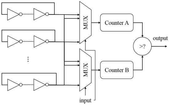
Figure 1.
The architecture of a traditional Ring Oscillator Physical Unclonable Function (RO PUF).
Few papers have discussed the impact of bias in RO PUF responses [], which is the favoring of RO PUFs to be either one or zero. According to our tests, we found that the counter design in the traditional RO PUF can contribute significantly to this bias. When and hold the same value, the comparator must make a choice of how to treat this case; in our example, the comparator puts this “equivalent” case in the “smaller” group. The “larger” group, on the other hand, can be active only when receives more pulses than in the given clock cycles. Therefore, the output will contain more zeroes than ones. If ROs are placed more regularly, the frequencies may end up being closer, thus causing more “equivalent” cases. This is aggravated especially when the counter size is limited. Regardless of the count cycles, the bias caused by the counter design is still as high as 5.03%. As a result, the bit error rate and the bias are intensified by the design fault and inaccurate measurement. Another problem of this RO PUF design is the inefficiency of hardware resource utilization. To generate only one bit of output, the design requires a -bit input and N oscillators. A transient effect of the ring oscillator PUF was proposed with a good ratio of PUF response variability to response length, but the intra-device variation increased to 1.7% [], compared to [], with 0.86% intra-device variation. In this paper, we will discuss a practical phase calibration technique to improve the quality of RO pairs’ comparison, which achieves a trade-off between the cost, stability and flexibility.
3. RO PUF Improvement and Implementation on FPGAs
Though RO PUFs have been heavily studied, there are still possibilities of improvement particularly with respect to implementations on FPGAs. In this section, we will discuss some practical hardware optimizations for RO PUFs.
3.1. RO PUF Design Improvement
While PUFs have been primarily targeted towards Application-Specific Integrated Circuits (ASIC) designs, in this paper, we explore their potential on FPGAs. According to our tests on the Kintex-7 FPGA [], the frequency of a five-stage inverter chain RO is approximately 475 MHz when the system clock is 200 MHz. In the crossing timing domain between the ROs and PUF control logic circuit, a high RO frequency adds to the instability of measurements. As with all oscillators, the rate of oscillation is determined by the length of a delay implemented in a loop. Thus, to reduce the frequency, more inverters can be added in the ROs, but this requires more hardware resources. In this work, we choose a design that takes advantage of the Lookup Tables (LUTs) of the Configurable Logic Blocks (CLBs) and the general purpose interconnect [] on the FPGA. As shown in Figure 2, the first part consists of a four-LUT delay and a one-LUT inverter. The reset signal is to control the enable timing of all LUTs. In the second part, a single inverter in the loop implements a high gain inverting amplifier. The output frequency is divided by two in order to eliminate output glitches. Overall, this architecture only needs six LUTs and a D-type Flip-flop (FD).
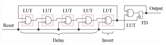
Figure 2.
The RO architecture for an FPGA implementation. FD, D-type Flip-flop.
In order to generate variable length responses, we choose a design as shown in Figure 3. This example uses 128 ROs to provide 128-bit CRPs. Once a challenge is received, it is stored in a shift register. We select the first seven bits from the register as the input of the upper decoder and MUX in order to select an RO from the array. Likewise, another RO is selected using the next seven bits from the challenge shift register. If the addresses are the same, the second seven-bit address is added by one to avoid selecting the same RO for comparison. Next, we shift the challenge register to select a new RO pair. The shift pattern can be complex for security consideration. To make it easy to understand, we shift one bit to the left each time. If the challenge is 128 bits, we can generate a 128-bit response with 127 shift operations.
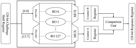
Figure 3.
Architecture of our RO PUF.
Alternatively, the shift register can be replaced by a non-cryptographic hash function. Compared to cryptographic hash functions, which have one-way, collision resistant and deterministic properties, a non-cryptographic hash function is significantly faster and low cost. It is also easy implement on FPGAs. Algorithm 1 shows the ElfHashexecution progress in our PUF:
| Algorithm 1 ElfHash process. |
|
In the traditional design, metastability can exist at the input of the counters. This occurs when the counters receive a clock rising edge for comparison. If the RO output happens to flip when a counter value is changing, the result of the comparison will not be larger, smaller or equal, but instead, a metastable state. We have verified this scenario on our FPGA implementations. Because of the metastability, the bit errors in the responses increase. Note that the counters receive RO output in the asynchronous timing, while their enable and disable are controlled by the system clock. Thus, the counter value becomes invalid if the measurement window closes at the input edge. The comparison result thus drops to the metastability state. Our solution is to use two registers to store the counter values. By involving a register that is in the same clock domain with the comparator, the counter can always provide a valid value before comparison. Therefore, the metastability is safely eliminated. Only larger, small and equal states are measured by the comparator. The corresponding result is recorded in the response register as an output bit.
3.2. RO PUF Implementation on an FPGA
Few papers have clear descriptions on how the RO PUF is implemented on FPGAs [,,]. Incorrect HDL coding can lead to logic unit rebuilding during synthesis, which results in functionality failure. For example, inverters built with inv(1) <= not inv(0); statements will be optimized out and cannot be placed as RO arrays. Therefore, to implement the ring oscillators on FPGAs, we use the LUTs directly in our code and add element placement constraints to fix the LUTs with a certain delay. In our work, we used the Vivado development kit and the Kintex-7 FPGA provided by Xilinx to show the RO PUF implementation on FPGAs [,]. In the Kintex-7, a CLB contains a pair of slices, and each slice is composed of four six-input LUTs and other elements []. By setting the initial value to “01”, a one-input LUT (LUT1) can perform the same function as a digital inverter. An example of the traditional RO implementation is shown in Figure 4. We place one LUT3 (three-input LUT) in the left slice and four LUT1s in the right slice. These five LUTs and the white connections form a basic RO. Apart from the feedback input of another inverter, LUT3 also includes a reset input and an enable input. The left LUTs in a CLB are reserved for other logic of the RO.
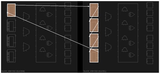
Figure 4.
LUT-based RO placement example.
Figure 5 shows the RO placement given by Figure 2. Four delay LUT2s are placed in the left slice, and the invert LUT is located in the right slice. The output of the first stage oscillator is connected to the FD, which builds another oscillator with another LUT2 in the right slice. Since the delay LUTs contain no logic, ‘keep’ attributes are required in the design to stop logic optimization by the synthesis tool. Additionally, a combinatorial loop in the FPGA is considered bad design practice in most cases, which increases the number of cycles by infinitely going around the circle in the same path. To avoid unnecessary errors during synthesis and bitstream generation, some constraints are applied to let Vivado ignore these loops.
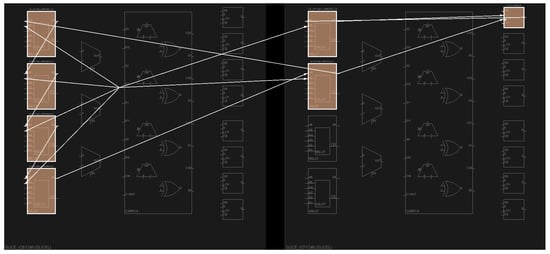
Figure 5.
Improved LUT-based RO placement example.
Figure 6 shows the manual placement of one RO PUF. To maintain the randomness and uniqueness, all the timing critical Flip-Flops (FFs)and LUTs must be placed carefully. One hundred twenty eight ROs are listed in six columns regularly in order to maximize the manufacturing differences between PUFs. Between columns, two slices are reserved for the relevant logic between ROs and the control unit. LUTs and FFs of the Finite-State Machine (FSM) are placed at the bottom of the RO array. Other primitives with no effects on the performance are placed by Vivado automatically.
Figure 6.
RO PUF manual placement overview.
However, manual placement of PUFs can be very time-consuming. In our example, each RO array contains 768 LUTs and 128 FFs. If the hardware specification is modified, it may lead to a reconstruction of the architecture. As a result, most of the cells have to be placed again. To make the progress more efficient, we show an automatic code generation process in Figure 7. The hardware specification module defines the length of CRPs, performance requirements and usable platforms. The information is translated to an acceptable format for the Shell script so that the code generation script knows the scale of the RO array. With pre-defined templates, we are able to generate the code and constraints automatically.
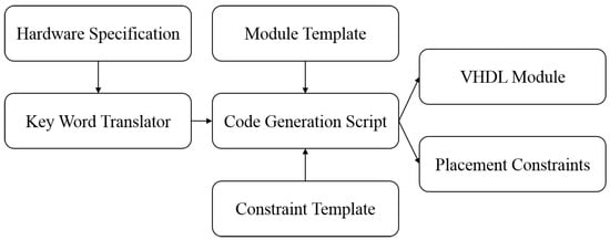
Figure 7.
RO PUF code generation.
On the other hand, improper routing also affects the uniqueness of PUFs. Though our LUT and FF placement constraints have fixed the internal routing path of each RO, the other parts are routed by Vivado automatically. The critical path is between the RO array enable and the counter enable. If the RO array enable has a long delay while the counter enable has a short delay, it indicates that the timing to generate RO pulses is postponed and the counter is enabled in advance. As a consequence, the window for measurement may not match the RO output well, which leads to the potential issues of uniqueness and bias. To eliminate the effect of unexpected delay, we adjust the unsatisfied wire delay by changing paths manually in the Vivado implementation user interface, which is saved in the constraints.
A key metric of any PUF is its reliability. In order to evaluate the stability, we have implemented three RO PUFs on the FPGA, which are based on Figure 3. We generated 100,000 random challenges and applied the challenge twice to each PUF. The two responses for each PUF were compared, and the Hamming distance between the two responses were recorded. Ideally, there should be no difference between the two responses because the challenge was the same and the Hamming distance should be zero. Figure 8 shows the Hamming distance distribution for the three PUFs. Without any error correction or fault tolerance methodology, there are about 10 bit errors in each 128-bit response. It is clear that a 7.81% bit error rate is unsatisfactory for authentication. Without very strong ECC, we will have a high false negative rate. To address the instability of PUFs, we will introduce a phase calibration process in the next section.
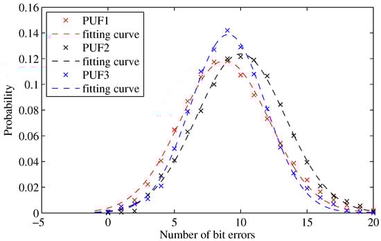
Figure 8.
Intra-PUF Hamming distance without ECC.
4. Phase Calibrated PUF
Improving the stability of PUFs requires an accurate measurement of the RO frequency. With the traditional RO PUF, theoretically, one could use a longer measurement time to count RO pulses and thus improve the measurement accuracy. However, we found that extending the measurement time from 16 clock cycles to 512, in order to get larger samples, had limited improvement on the stability. Since the ROs are not driven by the system clock and each enable signal has its own delay, the output can be unstable when the counter is enabled and disabled []. As a result, the count may be off by one or two. Previously, we discussed adding a counter register to eliminate the unknown state; this does not address the correctness due to instabilities at the boundaries of the measurement cycle. Due to this unpredictable behavior, even though we tested some “stable” RO pairs 1000 times and got the same results every time, the next measurement might still produce a different value with a small probability. In this section, we propose an efficient solution instead of the repeated testing, which can solve this problem with limited cost.
4.1. Phase Calibration Process
The Phase Calibration Process (PCP) is a critical part of our solution, which aims to measure the frequency of ROs quickly and accurately. The basic idea is to shift the phase of the RO output signal in order to eliminate asynchronous timing measurement error. To implement it on FPGAs, we use a primitive that offers a programmable delay function, i.e., Xilinx provides an input delay resource called IDELAYE2 []. It can be accessed directly from the FPGA logic and allows incoming signals to be delayed on an individual input pin basis. Figure 9 shows the IDELAYE2 primitive, which offers a variable delay mode that can control the delay value after configuration by manipulating the control signals CEand INC. When CE goes high, the increment/decrement operation begins on the next positive clock edge. The programmable delay taps into the IDELAYE2 primitive wrap-around. When the last tap delay is reached (Tap 31), a subsequent increment function will return to Tap 0. In Figure 9, a reset is detected (LDis High) in the first clock event, causing the output DATAOUT to select Tap 0 as the output from the 31-tap chain. In the second clock event, a pulse on CE and INC is captured on the rising edge of C. This indicates an increment operation. The output changes without glitches from Tap 0 to Tap 1. In the third clock event, CE and INC are no longer asserted, thus completing the increment operation. The output remains at Tap 1 indefinitely until there is further activity on the LD, CE or INC pins.
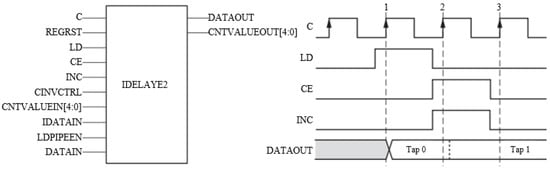
Figure 9.
Input delay resource and timing diagram.
The architecture of our Phase-Calibrated PUF (PCPUF) is shown in Figure 10. It mainly consists of a 128-RO array, a control unit, a comparison unit, a pair of decoders, MUXes, IDELAYE2s and counters. The tap control is to control the delay of IDELAYE2. Since PCP requires a strict RO enable timing, only one selected RO pair is enabled in the measurement period. Otherwise, the control unit resets all the ROs.
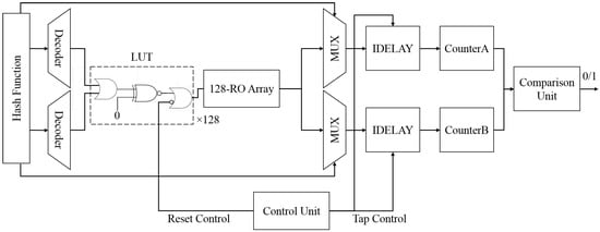
Figure 10.
Architecture of Phase-Calibrated PUF (PCPUF).
Algorithm 2 shows the details of the PCP. In order to generate a one-bit response, the first two seven-bit values of the challenge register are loaded to the register and register . After checking the values, we reset and . The tap value is loaded to IDELAYE2 primitives before being added by one. By default, the tap value is zero. When the delay is set, the control unit enables the selected RO pair and starts testing. Each measurement takes 16 clock cycles. Then, the tap value is added by one, and the new measurement starts. Between two measurements, the selected RO pair is kept disabled before the delay is set. When we complete the test from Tap 0 to Tap 31, a one-bit output is generated by comparing the counter values. Then, the challenge register shifts its value and launches the next response generation. Though the PCP slows down the response generation compared to the traditional RO PUFs, the PCPUF still keep an output speed of 625,000 bit/s.
| Algorithm 2 PUF phase calibration process. |
|
4.2. Analysis of Phase Calibration Efficiency
Considering the calculable factors of FPGA, the accuracy of frequency estimation by using the phase calibration process depends on the skew rate, threshold voltage and the relevant signal cycle. The skew rate and the threshold voltage determine the skew between the system clock and the counters. When the control unit enables or disables the counters at the beginning or at the end of the phase calibration process, the RO outputs may change between the voltage thresholds, and . This may lead to a metastable state of the counter value. According to the I/O buffer specification model of the Kintex-7, if the FFs are in the same bank, the skew should be 50 ps to 100 ps. The internal signal voltage of the Kintex-7 is designed to swing between −0.5 and 1.1 volts, with anything below 0.4 volts considered a ‘0’ and anything above 0.7 volts considered a ‘1’ []. In the worst case, the metastability duration of each rising edge or falling edge is 18.75 ps. Since the RO output phase at the beginning of the window is unpredictable, we can calculate the probability of the metastability occurrence in Figure 11 as:
in which 4210 ps is the average RO cycle. Though the rising edge and falling edge have the same probability, they are not independent events for any RO within one tap delay. Now, we focus on the entire process in Figure 11. We create a window of 16 system clock cycles (80 ns), within which the counters of the RO PUF become active. Due to the wire delay, the selected RO pair may not be enabled at the same time. The delay between each RO and the related counter depends on a tap ranging from zero to 31. Since each tap of IDELAYE2 offers a 78-ps delay in the normal environment, we can have as much as a 2.418-ns delay of the RO output, which is long enough to find the metastability. Ideally, these 32 taps’ phase shift will not affect the RO frequency measurement. However, some measurements show different counter values due to the metastability. According to our simulation, one metastability occurrence at one edge of the window has a probability of 0.00775. The probability of two metastability occurrences at both edges of the window is 0.00113. There is no possibility of any more unpredictable states as the window only has two edges. Thus, the expected value of metastability is:
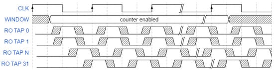
Figure 11.
PUF phase calibration timing.
Therefore, among the 32 taps’ shift cases, most of the counter values reflect the frequency of the selected RO correctly. The metastability only happens with a very low possibility.
Apart from the calculable factors, measurement errors are also generated by the noise margin, which is the amount by which the signal exceeds the threshold for a proper ‘0’ or ‘1’. Being affected by uncontrollable factors such as temperature, voltage and aging effects, we can hardly calculate the fault tolerance capability of the phase calibration process directly []. However, we are able to obtain the probability of bit flipping after PCP through large amounts of tests. Next, we estimate the efficiency of PCP by computing the intra-PUF Hamming distance.
4.3. Estimation of Intra-PUF Hamming Distance
The bit error rate is one of the most critical characteristic of PUFs. To estimate the RBER of PCPUFs, we need to know the intra-PUF Hamming distance first, which can be calculated through the distributions of RO frequencies and the Bit Flipping Rate (BFR). As we mentioned, when the frequencies of two ROs are closer, temperature, voltage and aging effects during operation lead to higher BFR. We begin with measuring the rising edges of ROs in the unit time and show the probability distribution in Figure 12. The unit time is set to 80 ns (16 clock cycles). Since we add the measured data from Tap 0 to Tap 31 and compute the average value, the results may not be integral. A fitting Gaussian curve is generated according to the discrete data, which are used to provide an ideal discrete distribution for our computation.
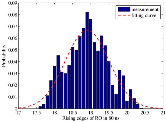
Figure 12.
Distribution of RO rising edges on average.
We define a specific bit flipping rate according to the difference of the discrete data. Marked as and , the frequencies of two ROs determine the probability of bit flipping. A measured in Figure 13 shows the statistical BFR results, which follows part of a normal distribution . When two ROs have a larger than one, their output is very stable. However, the BFR increases sharply when the difference range is less than 0.5. To further improve the reliability of PUFs, these RO pairs can be blocked from the RO pair selection sets.
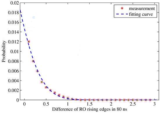
Figure 13.
Distribution of one-bit RO output flipping rate.
For any single bit, the probability of error occurrence can be computed as:
The probability that 128-bit responses contain exactly n bit errors is:
According to Equation (4), the ideal intra-PUF Hamming distance is shown in Figure 14. Therefore, we can calculate the average number of errors, which is 0.3688 in a 128-bit response.
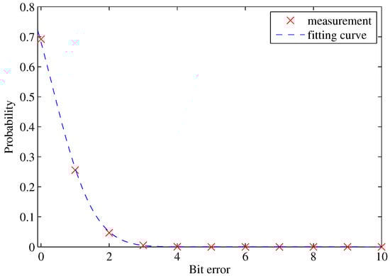
Figure 14.
Expected intra-PUF Hamming distance.
5. PCPUF Application
PUFs are well known to be used for authentication. In this section, we explore the feature of PCPUFs and propose new strategies to generate secure responses. We also discuss their authentication application.
5.1. Unstable-Stable Response
Modeling and machine learning attacks are well known for PUF adversaries. The successful prediction is due to the accurate calculation and measurement of physical parameters such as delay and frequency. To achieve a secure PUF-based solution against those attacks, we propose a novel method to generate responses, which uses the instability of PUFs. Since the unstable bits in the RO PUF response are hard to predict, they provide a better security guarantee than the stable ones. In the past, these unstable bits have been simply considered for random number generation applications. For other scenarios, only stable bits are usually required. In our work, we find the possibility to transfer unstable bits to stable bits and apply them to PUF responses, which are presented as Unstable-Stable Responses (USR), a more stable and secure response.
Figure 15 shows how to generate USR with a PCPUF. We set another hash function module out of the PCPUF, which can provide multiple sub-challenges with only one challenge input. Once a sub-challenge is created, it is sent to the challenge register for temporary storage. By reading the value from the register, PCPUF selects two RO pairs and keeps outputting the one-bit response to the first address of the unstable bit counter 1000 times. The accumulated value in the counter reflects the stability of this output. A number that is close to zero or 1000 is known to be stable, while 500 is regarded as the most unstable. With the help of the internal hash function module, the model generates a 128-bit raw response and stores it in the counter. Since PCPUFs provide good stability in their responses, the obvious unstable bits become so limited that less than one unstable bit can be found in 128 bits. In the unstable bit counter, we mark the unstable bits as ‘1’ and stable ones as ‘0’. The counter records the number of ones and sends the 128 bits to the response register. Obviously, a 128-bit response marked with only unstable bits is highly-biased towards zeroes. Therefore, the counter enables the hash function module in order to launch the next progress with a different internal challenge. Another raw response is generated and transferred to an internal response in the counter. We apply a bitwise OR operation to this internal response and the one that was previously stored in the response register. After updating the register value, the new response should have a higher probability of containing more ones. By repeating the same process, the response in the register will eventually reach a balance between ‘1’ and ‘0’. Now, it is ready to serve as the final response.
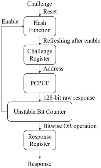
Figure 15.
Generating stable responses by using unstable raw responses.
Note that the current design cannot guarantee a static threshold of how many times the process should be executed. The first reason is that the unstable bits selected by the hash function module are not controllable. Secondly, the ones in two responses may be overlapped. Thus, the amount of ones is reduced by the OR operation. To estimate the threshold, we define u as the number of unstable bits in the 128-bit internal response. The probability that a certain bit is not set to ‘1’ in one process is . If we assume that the process in Figure 15 is repeated n times, the probability that the bit is not set to ‘1’ after n process iterations is:
The probability that it is ‘1’ is therefore:
Given the 128 bits in the complete response, we should have on average 64 ones and 64 zeroes. Since the 128 bits are independent, we can calculate the expected number of ones as . In order to have the expected 64 ones, should thus equal . Plugging in Equation (6), we can calculate that n should be:
By solving the equation, we are able to set a reasonable threshold in order to control the bias. When the unstable bits is 0.5%, n is about 138. Though it is possible to control the bias with a dynamic adjustment, the required logic resources will increase significantly. This strategy can be applied to different PUFs for stability improvement.
5.2. USR-Based Authentication
As a well-known application of PUFs, authentication does not require a very low bit error rate of the PUF responses. Thus, we can apply our USRs directly to the solution. For the simplest authentication, we compare two responses and check if the mismatched bits are larger than a threshold t. In this application, the false negative rate and false positive rate are critical for performance evaluation. Given a bit error rate e in 128-bit USRs, the false negative should be:
On the other side, the false positive is:
in which p is the probability of a random collision in 128 trials. Ideally, the value is close to 0.5.
Apart from the accuracy, we also need to estimate the cost of this solution. One important aspect is the utilization of the memory space. In the simplest solution, we do not require ECC as the bit error rate in USRs is very low. Thus, there is no additional overhead except the CRPs. Given the CRP length of n, the memory cost is 2n bits per CRP. This is acceptable for small amounts of authentication requests. However, as the requests grow, the memory cost increases linearly. A lightweight solution is to record the instability information of PUFs instead of CRPs. The assumption is that we trust the security of the database, which contains some sensitive information of PUFs. In that case, we can calculate the USRs with the known hash function, instability RO pairs and the corresponding challenges.
As we mentioned above, an effective solution is based on the assumption that the database is secure. However, we must consider the scenario that the information is disclosed to attackers. The typical solution is to encrypt the database. Alternatively, we can choose a solution that combines the ECC and Bloom filter [], which is both secure and efficient.
5.3. Obfuscation-Based Authentication
Since some authentication applications require a higher security level, we provide another scheme for our PUFs with a strong obfuscation. Our prime goal is that even if a current response is disclosed, it does not leak non-negligible information about the next responses with the same challenge, which means attackers cannot use the replay attack to pass the authentication when a repeated challenge is applied. Secondly, the scheme has strong modeling attack resistance by involving unstable bits in the responses, but the authentication accuracy will not be affected in the database. Furthermore, though probe attacks can obtain the information, the final response is still unpredictable.
The scheme starts from the N-bit challenge register in Figure 16. Before launching the challenges, a PCPUF stability model is created in the hardware memory. It records the stable RO pairs and unstable ones. After a challenge is received from the database, the register value will not be updated until the final response is generated. In the first loop, the challenge is hashed by a one-way hash function module with an initial seed. The hash value is sent to the secure address generator as a secure challenge. By mapping the generated addresses to the PCPUF stability model, we select stable bits and one very unstable RO pair. We enable the unstable RO pair in order to generate one-bit output for obfuscation. The position of the inserted unstable bit depends on the hash value. The N-bit temporary response is saved in . Then, we apply the exclusive or operation to the value between and and store the result in . In the first loop, the value in is zero as it is reset along with a new challenge. Since the secure address generator knows the selected stable bits, they are sent to the one-way hash function module and hashed as the secure challenge of the second loop. Before the hash operation, a one-bit ‘0’ is added to the end of the stable bits to ensure that the input length is N-bit. This process repeats T times to generate the final response. In the loop t, the secure address generator still selects stable bits and one unstable RO pair, which is stored in . However, there are t accumulated unstable bits in , given the different inserted positions by the secure address generator. As Algorithm 3 showed, the final response contains T unstable bits.
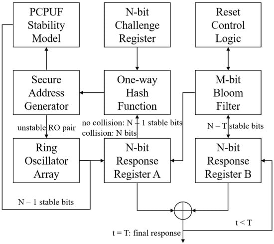
Figure 16.
Secure obfuscation-based authentication solution.
To check the collision, we involve a Bloom filter and its reset control logic module in our scheme. A Bloom filter is a space-efficient probabilistic data structure that is used to test whether an element is a member of a set. With an obfuscation bit mask from the secure address generator, the stable bits are sent from to the Bloom filter. After being added by T-bit zeroes, the string is hashed by k hash functions, and the hashed values are stored in an M-bit Non-Volatile Memory (NVM) Bloom filter. The NVM should be tamper resistant against any malicious reset. Whenever a final response is generated, we check the Bloom filter first to ensure that the response has never been released before. If there is no collision, we update the Bloom filter with the k hash values and output as the final response. However, once a collision is found, the final response will be stalled in . As a further obfuscation, we rerun this process for T times to generate a new response. However, this time, we switch the hash function input to the entire , which means the unstable bit is included in the one-way hash input. After T loops, the final response will hardly disclose any information of the PUF state and pattern.
Due to memory space limitation, it is not possible to store infinite hash values in the NVM. Therefore, we use a reset control logic to clean the Bloom filter when the false positive reaches a preset threshold. According to our scheme, the PUF is not allowed to generate the same response twice within the threshold times. Modeling attacks are also inefficient as stable response bits, and the internal state is obfuscated by the unstable bits, one-way hash function and the Bloom filter. Even if the Bloom filter is reset, the pattern cannot be detected due to the T times one-way hashing. The complexity of our scheme also makes probe attacks useless since the next final response is unpredictable given a known PCPUF model, Bloom filter content and the current register value. Since the attackers cannot try all input patterns when N is large, our scheme is secure.
To authenticate our PUFs in a secure way, we avoid recording any data in the database that may disclose the information of the PUFs. Instead, we use Bloom filters for authentication, in which the hash functions provide strong resistance against software reverse engineering. When a PUF is manufactured, we test the PUF and store the PCPUF stability model in the database. Then, we redo the response generation process by software, with our challenge set and the known initial seed in the PUF. Since we cannot predict the unstable bits in the response, all the possibilities must be generated by an authentication tree, as shown in Figure 17. The responses of are generated after the first loop of calculations according to the challenge . and are based on the assumption that the obfuscating unstable bit is ‘0’ and ‘1’. In the second loop, the responses of are generated with the stable bits from , and the unstable bits lead to four combinations. By following this progress, we obtain possibilities of the final response. With the same challenge , the final response of this PUF must belong to the set of . Thus, all the responses in this set need to be recorded in the Bloom filter with as one-time CRP. As we apply nonce to the challenge set, it is not necessary to calculate and store the final response set of the second T loop. By mapping the response set with one-way hash functions, we can guarantee the data security in the database.
| Algorithm 3 Secure authentication scheme. |
|
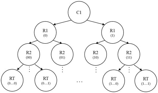
Figure 17.
PUF authentication tree in the database.
This security scheme sacrifices hardware resources, however. For instance, after generating one million responses, the Bloom filter will be reset to maintain a false positive of . The size of NVM and the number of hash functions are calculated as:
In the database, the false positive rate of the Bloom filter affects the authentication accuracy. Thus, it needs to be much lower than that in the PUF. If we set it to , the size of Bloom filter for one million CRPs is:
Obviously, the cost is higher than the USR-based authentication solution. In summary, there is always a trade-off between the cost and the security. Those low-cost solutions are suitable for a large amount of chips, while this scheme enhances the security level for some critical applications.
6. Experimental Results
In this section, we present the measured data from six implemented PCPUFs on two KC705 boards, as shown in Figure 18. The temperature of FPGAs was controlled at 30 °C according to the on-chip sensor, and the voltage was 1.008 V. Table 1 lists the post-implementation primitive utilization of the traditional RO PUF with the shift register and the optimized PCPUF. We excluded the UART and FIFO module in the design to make a fair evaluation. The overall utilization of our PCPUF was 0.58% of the look-up tables and 0.05% of the flip-flops on the Kintex-7 FPGA. We cannot compare our PC PUF design with a traditional RO PUF architecture (Figure 1), because only 35 RO arrays can be placed on a Kintex-7 FPGA, which means four FPGAs are required to provide enough area for a 128-bit traditional RO PUF implementation. By using a shift register or hash function in our design, we are able to easily generate 128-bit responses in a fraction of a single FPGA.
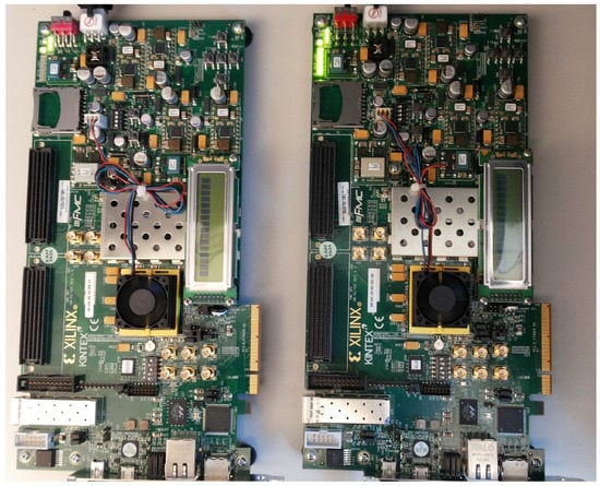
Figure 18.
PCPUF tests on KC705 boards.

Table 1.
FPGA resource usage of the shift-register RO PUF and the optimized PCPUF implementations for a 128-bit response. Traditional RO PUF cannot be implemented on FPGAs for 128 bits. CLB, Configurable Logic Block.
6.1. Randomness
We applied 15 NIST randomness tests to evaluate the randomness of our PCPUF responses. The p-values and proportions are listed in Table 2. As the p-values were all larger than 0.01, we accepted the responses as random []. Though we used a pseudorandom number generator to generate challenges, the proportions showed that at least 98% of sequences passed the tests.
Table 2.
Results of NIST randomness tests.
6.2. Uniqueness
The evaluation of the uniqueness of PCPUFs is shown in Figure 19, which compares three groups of 100,000 128-bit responses. The responses were generated by downloading the same bitstream to two different Kintex-7 FPGAs. The fitting curves had a converging to 64; thus, there were 50% bits flipped on average. Therefore, the responses were unique. Moreover, we have compared the responses from six PUFs on two FPGAs, and they all followed a normal distribution.
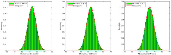
Figure 19.
Inter-PUF Hamming distance.
6.3. Stability
As shown in Section 4, the average number of errors was 0.3688 in 128-bit responses, which means the theoretical bit error rate was 0.29%. To verify that, we generated challenges with a pseudorandom number generator. Each challenge was used twice in order to provide two responses for comparison. The test was repeated 100,000 times. Figure 20 shows the measured intra-PUF Hamming distance of our PCPUFs. Compared to the corresponding results with no ECC and phase calibration in Figure 8, the fitting curves for PCPUFs have an obvious shift to the left and approach the ideal bound in Figure 14.
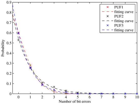
Figure 20.
Intra-PUF Hamming distance with phase calibration.
Table 3 shows the average bit error rate of three shift register-based RO PUFs and six PCPUFs. Compared to RO PUFs, PCPUFs have an obvious improvement on the response stability. Though the bit error rates were higher than the ideal bound, all the results were smaller than 1.00%. This is still acceptable if we take the measurement errors into consideration. Since we did not apply ECC in our PUFs, the bit error rate was low enough for authentication purposes. Within the temperature range of a normal testing environment, we observed no significant changes of the bit error rate.
Table 3.
Bit Error Rate (BER) of RO PUFs and PCPUFs.
We compare the stability of PCPUF with four novel FPGA-based PUF implementations in Table 4. The improved configurable RO PUF is known for ID generation with a strict Hamming distance []. The composite PUF was developed for a larger challenge space and superior quality metrics with acceptable resource requirements []. Another improved RO PUF was proposed in [], which was capable of generating multiple output bits from each RO pair and allowed one to create a higher number of pairs of ROs. The last one applies the Full Scan Technique (FST) on different numbers of RO stages to determine the one with the highest diverseness of RO frequencies []. Compared to these RO PUF designs with their own advantages, our work focused on the improvement of stability. Therefore, it provided a lower bit error rate in the responses.
Table 4.
Bit error rate Comparison of different PUF implementations on FPGAs.
6.4. Bias
Ideally, there should be 50% ones and 50% zeroes in a response. However, our RO PUF implementation on Kintex-7 FPGAs had a bias ranging from 41% to 58% according to our tests. As a comparison, we list the bias of PCPUFs in Table 5. Each result was based on the mean of 100,000 128-bit responses. Without any post-processing, all six PUFs produced bias within ±2% of ideal, which proves the effectiveness of the phase calibration on the improvement of the RO PUF bias.
Table 5.
Bias of RO PUFs and PCPUFs.
6.5. Authentication Application
The performance of USR-based authentication is shown in Table 6. Compared to the measured raw response of PCPUFs, USRs had a lower bit error rate. When we set the threshold to 20, all three PCPUFs had a low false positive and false negative rate in theory. We also verified the bound by measuring 300,000 CRPs on an FPGA. The results showed that no false positive or false negative was detected.
Table 6.
False positives and false negatives of USR-based authentication.
Table 7 shows the other authentication solutions with Hamming ECC and Bose-Chaudhuri-Hocquenghem (BCH)ECC. Hamming(255,247) could correct one bit error in 128-bit responses, while BCH(255,128,15) had a correct capability of as many as 15. However, the overhead of BCH ECC was much larger than that of Hamming ECC. We applied both ECCs to the shift register-based RO PUFs and our PCPUFs. Compared to the poor performance on RO PUFs, the lower bit error rate of PCPUFs took better advantage of ECCs. When those 100,000 CRPs were tested with BCH ECC, no false negative was detected. Though it is hard to estimate the accurate false negatives of BCH ECC-based authentication on PCPUFs, we can compare the overhead of these solutions in order to find a better trade-off. The codeword of BCH ECC was almost the same size as the key, while our USR-based solution had no additional overhead at all. Therefore, USR-based authentication is recommended when the memory space becomes a critical bottleneck.
Table 7.
Performance of ECC-based authentications.
7. Conclusions
In this paper, we demonstrated a practical design and implementation of RO PUFs on FPGAs. Our main contribution was the phase calibration process, which focused on improving the frequency measurement techniques in the crossing clock domain area. By using a phase calibration process, the 7.81% bit error rate was reduced to less than 1%. Another contribution was the application of instability in PCPUFs. By using the unstable RO pairs as stable responses and obfuscation, we improved the stability and security of PCPUF-based authentication.
Author Contributions
Conceptualization, Y.W. and C.J. Methodology, Y.W. Software, Y.W. Validation, Y.W. and C.J. Formal analysis, Y.W. Investigation, Y.W. Resources, Y.W. Data curation, Y.W. Writing, original draft preparation, Y.W. Writing, review and editing, C.J. Visualization, C.J. Supervision, C.J. Project administration, C.J. Funding acquisition, C.J.
Funding
This research was funded by National Science Foundation grant number DGE-1318964. Any opinions, findings and conclusions or recommendations expressed in this material are those of the authors and do not necessarily reflect those of the National Science Foundation.
Conflicts of Interest
The authors declare no conflict of interest.
References
- Suh, G.E.; Devadas, S. Physical Unclonable Functions for Device Authentication and Secret Key Generation. In Proceedings of the 44th ACM/IEEE Design Automation Conference, San Diego, CA, USA, 4–8 June 2007; pp. 9–14. [Google Scholar]
- Herder, C.; Yu, M.D.; Koushanfar, F.; Devadas, S. Physical Unclonable Functions and Applications: A Tutorial. Proc. IEEE 2014, 102, 1126–1141. [Google Scholar] [CrossRef]
- Gassend, B. Physical Random Functions. Ph.D. Thesis, Massachusetts Institute of Technology, Cambridge, MA, USA, 2003. [Google Scholar]
- Guajardo, J.; Kumar, S.; Schrijen, G.J.; Tuyls, P. FPGA Intrinsic PUFs and Their Use for IP Protection. In Cryptographic Hardware and Embedded Systems—CHES 2007; Lecture Notes in Computer Science; Paillier, P., Verbauwhede, I., Eds.; Springer: Berlin/Heidelberg, Germany, 2007; Volume 4727, pp. 63–80. [Google Scholar]
- Kumar, S.S.; Guajardo, J.; Maes, R.; Schrijen, G.J.; Tuyls, P. The butterfly PUF protecting IP on every FPGA. In Proceedings of the IEEE International Workshop on Hardware-Oriented Security and Trust, HOST 2008, Anaheim, CA, USA, 9 June 2008; pp. 67–70. [Google Scholar]
- Rahman, M.T.; Forte, D.; Rahman, F.; Tehranipoor, M. A pair selection algorithm for robust RO-PUF against environmental variations and aging. In Proceedings of the 2015 33rd IEEE International Conference on Computer Design (ICCD), New York, NY, USA, 18–21 October 2015; pp. 415–418. [Google Scholar]
- Maiti, A.; Casarona, J.; McHale, L.; Schaumont, P. A large scale characterization of RO-PUF. In Proceedings of the 2010 IEEE International Symposium on Hardware-Oriented Security and Trust (HOST), Anaheim, CA, USA, 13–14 June 2010; pp. 94–99. [Google Scholar]
- Merli, D.; Stumpf, F.; Eckert, C. Improving the quality of ring oscillator PUFs on FPGAs. In Proceedings of the 5th Workshop on Embedded Systems Security, Scottsdale, AZ, USA, 24 October 2010; p. 9. [Google Scholar]
- Yu, H.; Leong, P.H.W.; Hinkelmann, H.; Moller, L.; Glesner, M.; Zipf, P. Towards a unique FPGA-based identification circuit using process variations. In Proceedings of the 2009 IEEE International Conference on Field Programmable Logic and Applications, Prague, Czech Republic, 31 August–2 September 2009; pp. 397–402. [Google Scholar]
- Maiti, A.; Schaumont, P. Improving the quality of a physical unclonable function using configurable ring oscillators. In Proceedings of the 2009 IEEE International Conference on Field Programmable Logic and Applications, Prague, Czech Republic, 31 August–2 September 2009; pp. 703–707. [Google Scholar]
- Yin, C.E.; Qu, G.; Zhou, Q. Design and implementation of a group-based RO PUF. In Proceedings of the Conference on Design, Automation and Test in Europe, Grenoble, France, 18–22 March 2013; EDA Consortium: San Jose, CA, USA, 2013; pp. 416–421. [Google Scholar]
- Bossuet, L.; Ngo, X.T.; Cherif, Z.; Fischer, V. A PUF based on a transient effect ring oscillator and insensitive to locking phenomenon. IEEE Trans. Emerg. Top. Comput. 2014, 2, 30–36. [Google Scholar] [CrossRef]
- Xilinx. 7 Series FPGAs Configuration User Guide; Rev. 1; Xilinx: San Jose, CA, USA, 2016. [Google Scholar]
- Xilinx. Frequency Counter for Spartan-3E Starter Kit; Rev. 2014.1; Xilinx: San Jose, CA, USA, 2006. [Google Scholar]
- Machida, T.; Yamamoto, D.; Iwamoto, M.; Sakiyama, K. A New Arbiter PUF for Enhancing Unpredictability on FPGA. Sci. World J. 2015. [Google Scholar] [CrossRef] [PubMed]
- Wild, A.; Becker, G.T.; Güneysu, T. On the problems of realizing reliable and efficient ring oscillator PUFs on FPGAs. In Proceedings of the 2016 IEEE International Symposium on Hardware Oriented Security and Trust (HOST), McLean, VA, USA, 3–5 May 2016; pp. 103–108. [Google Scholar]
- Xilinx. Vivado Design Suite User Guide; Rev. 1; Xilinx: San Jose, CA, USA, 2014. [Google Scholar]
- Xilinx. 7 Series FPGAs Configurable Logic Block User Guide; Rev. 1.7; Xilinx: San Jose, CA, USA, 2014. [Google Scholar]
- Xilinx. 7 Series FPGAs SelectIO Resources User Guide; Rev. 1.6; Xilinx: San Jose, CA, USA, 2015. [Google Scholar]
- Xilinx. Kintex-7 FPGAs Data Sheet: DC and AC Switching Characteristics; Rev. 2.15; Xilinx: San Jose, CA, USA, 2015. [Google Scholar]
- Maiti, A.; McDougall, L.; Schaumont, P. The Impact of Aging on an FPGA-Based Physical Unclonable Function. In Proceedings of the 2011 International Conference on Field Programmable Logic and Applications (FPL), Chania, Greece, 5–7 September 2011; pp. 151–156. [Google Scholar]
- Yan, W.; Tehranipoor, F.; Chandy, J.A. A Novel Way to Authenticate Untrusted Integrated Circuits. In Proceedings of the IEEE/ACM International Conference on Computer-Aided Design, Austin, TX, USA, 2–6 November 2015; IEEE Press: Piscataway, NJ, USA, 2015; pp. 132–138. [Google Scholar]
- National Institute of Standards and Technology. A Statistical Test Suite for Random and Pseudorandom Number Generators for Cryptographic Applications; Rev. 1a; National Institute of Standards and Technology: Gaithersburg, MD, USA, 2010.
- Xin, X.; Kaps, J.P.; Gaj, K. A configurable ring-oscillator-based PUF for Xilinx FPGAs. In Proceedings of the 2011 14th IEEE Euromicro Conference on Digital System Design (DSD), Oulu, Finland, 31 August–2 September 2011; pp. 651–657. [Google Scholar]
- Sahoo, D.P.; Saha, S.; Mukhopadhyay, D.; Chakraborty, R.S.; Kapoor, H. Composite PUF: A new design paradigm for Physically Unclonable Functions on FPGA. In Proceedings of the 2014 IEEE International Symposium on Hardware-Oriented Security and Trust (HOST), Arlington, VA, USA, 6–7 May 2014; pp. 50–55. [Google Scholar]
- Kodỳtek, F.; Lórencz, R.; Buček, J. Improved ring oscillator PUF on FPGA and its properties. Microprocess. Microsyst. 2016, 47, 55–63. [Google Scholar] [CrossRef]
- Mustapa, M.; Niamat, M. Relationship between Number of Stages in ROPUF and CRP Generation on FPGA. In Proceedings of the International Conference on Security and Management (SAM), Las Vegas, NV, USA, 21–24 July 2014; p. 1. [Google Scholar]
© 2018 by the authors. Licensee MDPI, Basel, Switzerland. This article is an open access article distributed under the terms and conditions of the Creative Commons Attribution (CC BY) license (http://creativecommons.org/licenses/by/4.0/).