1. Introduction
The continuous growth of modern computing applications including digital signal processing, embedded systems, microsystems, artificial intelligence hardware, and high-performance computing has substantially raised the demand on low and energy-efficient arithmetic units [
1,
2]. Multiplication is one of the most basic arithmetic operations in most computational tasks, such as filtering, image processing, cryptographic algorithms and computations of neural networks [
3]. Since these applications often have many multiplication operations, optimizing the architecture of efficient multiplier design has been a significant research area in advanced computing systems [
4].
Signal processing is fundamental across many areas of engineering because it enables extracting meaningful information from raw signals through interpretation, filtering, and analysis [
5]. It is highly popular in multimedia, real-time embedded processing platforms, industrial monitoring, and communications and sensing systems [
6]. Due to the ubiquity of edge and IoT devices, signal-processing tasks are being performed with strict limits on both latency, power, and hardware area, and computational efficiency is becoming a key design goal [
7]. Practically, interference, quantization effects, and environmental variations will often corrupt signals; consequently, advanced processing methods are needed to maintain the level of reliability and make downstream decisions that can be trusted. Here, effective arithmetic, especially multiplication, is critical to the realization of major kernels including filtering, correlation, transforms and feature extraction [
8].
Real-world signals can be susceptible to environmental sources of interference. These degradations have the potential of greatly impairing the accuracy of interpretation and thus necessitate robust digital signal-processing methods to obtain credible information from the data obtained [
9]. The filtering and feature extraction, specifically, require the use of efficient arithmetic hardware, and in particular, multiplier units due to the presence of numerous core operations dominated by computations [
10]. In the past, the procedure of digital signal processing has been based on the usage of complementary metal-oxide-semiconductor (CMOS)-based multipliers, although this type of circuit is associated with high power usage, bigger transistor density, and non-trivial signal propagation delay, which restricts scaling in energy- and area-constrained real-time systems [
11]. Moreover, sustained high-throughput computation under strict energy budgets further exposes the limitations of conventional CMOS technology for next-generation compact and low-power platforms.
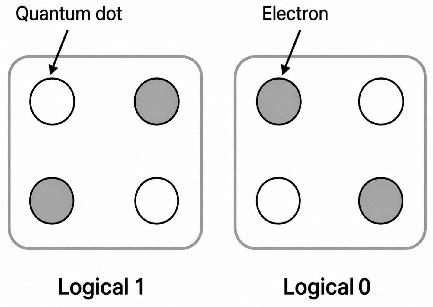
Quantum-dot cellular automata (QCA) is a potential alternative, offering ultra-low power consumption, high-speed switching, and smaller circuit area due to the absence of conventional transistors and the use of Coulombic interactions among quantum dots [
12]. In QCA, the data stored is encoded via the polarization of the quantum dots, where two different charge configurations are mapped to logic ‘1’ and logic ‘0’ as illustrated in
Figure 1 [
12]. Unlike conservative transistor-based logic, which can only achieve such through the merit of higher transistor counts, QCA depends on Coulombic connections among quantum dots to perform computations, leading to far reduced power consumption and higher processing speeds [
12].
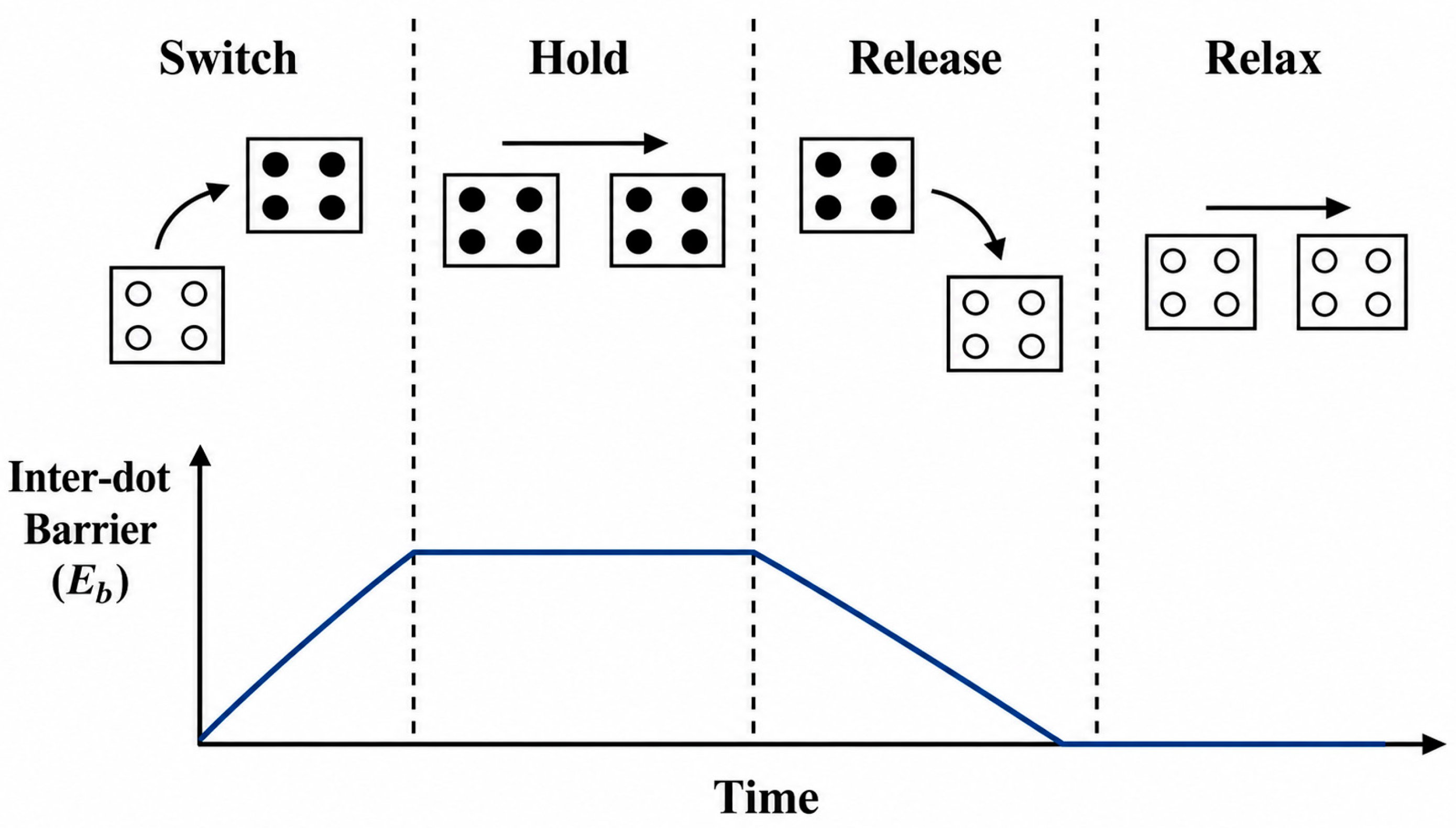
QCA clocking is a compactly designed clock mechanism that controls the flow and synchronization of data in QCA circuits. In contrast to conventional clocking in CMOS, a four-phase clocking arrangement is used in QCA: Switch, Hold, Release, and Relax, as illustrated in
Figure 2 [
13]. In particular, the phases set the polarization of the quantum dots to ensure signal propagation while also preventing unwanted interference. In addition to allowing the data to move similarly, the QCA clock also reduces latency by allowing for pipelining. Clocking zones also aid in defining circuit timing, decreasing latency, and improving fault tolerance in the complex QCA architecture [
14,
15].
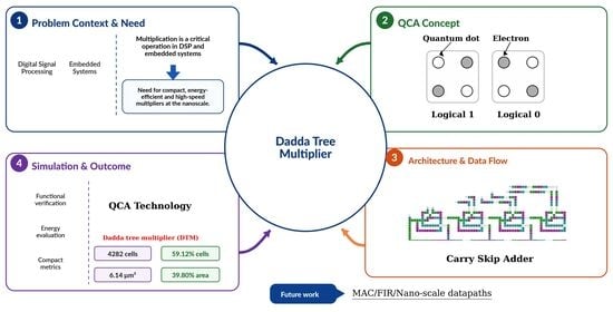
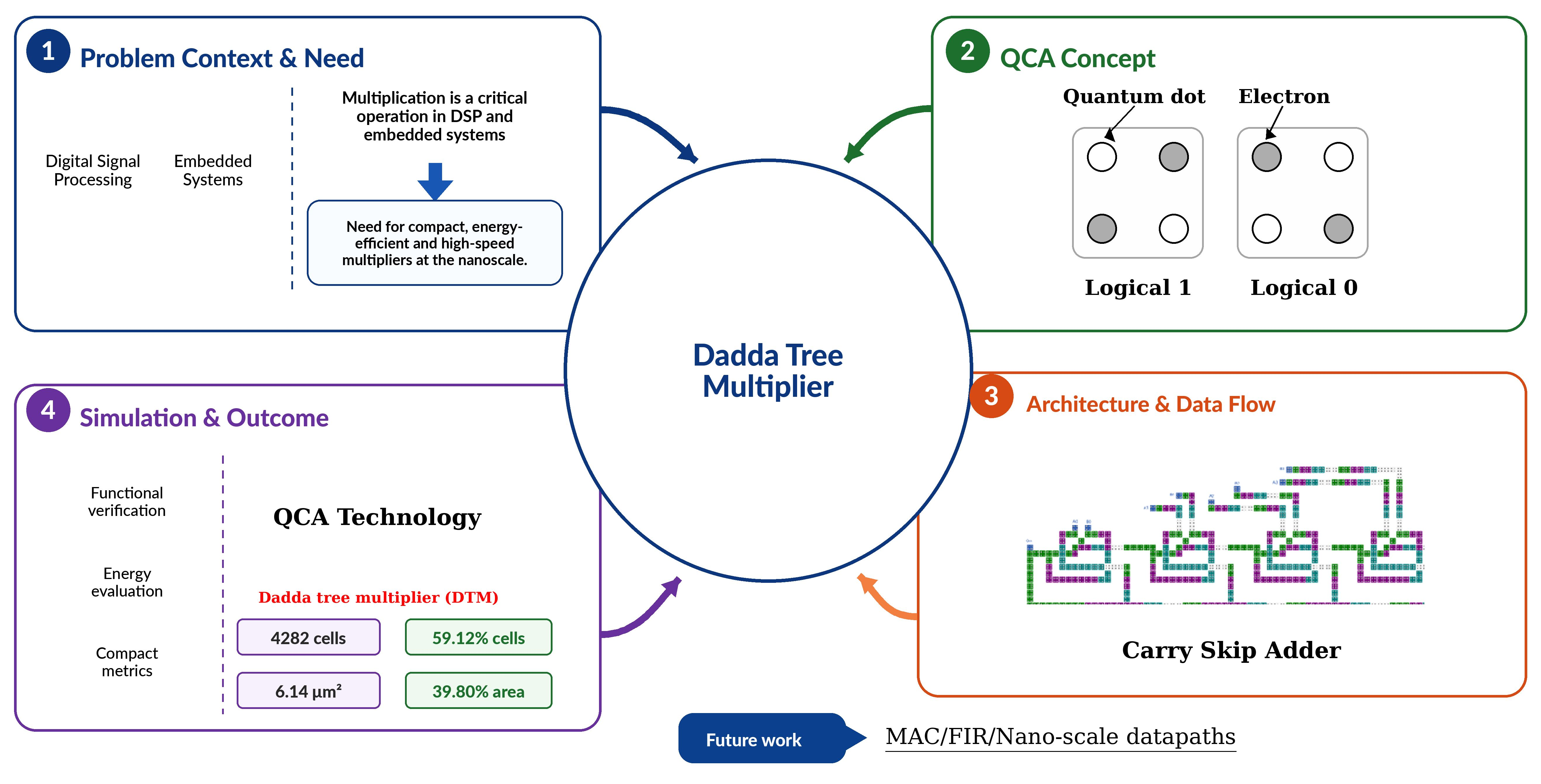
This work highlights the capability of QCA-based arithmetic circuits to satisfy the strict requirements of next-generation nanoscale computing platforms, where area, energy, and latency must be simultaneously optimized. We proposed a scalable nanoscale Dadda Tree Multiplier (DTM) designed for high-throughput signal-processing workloads in embedded systems. The architecture follows a designed partial-product reduction strategy and is realized using a layout-aware integration of an optimized carry-skip adder stage, together with efficient full adder (FA), half-adder (HA), and XOR modules, enabling faster accumulation with reduced routing overhead and shortened critical paths. The suggested DTM is designed and verified in QCADesigner 2.0.3 resulting in a small implementation of 4282 cells on 6.14 μm2. Compared with a recent compact QCA multiplier baseline, the design delivers a 59.12% reduction in cell count and a 39.80% reduction in occupied area, while maintaining fast propagation characteristics suitable for nanoscale arithmetic. These results confirm that the proposed QCA-DTM provides a practical and efficient multiplication core for emerging nano-computing and real-time signal-processing systems. This article’s main contributions are summarized below:
A compact single-layer QCA-based DTM is designed for nanoscale arithmetic and embedded signal-processing workloads.
A layout-aware integration strategy is developed by combining compact HA, FA, XOR, and CSA modules to reduce routing overhead and propagation delay in a single-layer realization.
The Dadda reduction process is implemented in QCA by organizing partial-product compression and final accumulation stages under clock-aware layout constraints.
The proposed design is functionally verified using QCADesigner 2.0.3, and its energy behavior is evaluated using QCADesigner-E.
A comparative analysis is provided in terms of cell count, occupied area, clocking latency, cost, energy, power, and Power-Delay Product (PDP) against representative QCA arithmetic designs.
The rest of the paper is structured as follows:
Section 2 reviews related work on QCA-based multiplier circuits.
Section 3 presents the recommended designs consisting of adder circuits, CSAs and DTMs. Moreover,
Section 4 briefly explains simulation results and comparative analysis. Lastly,
Section 5 concludes the manuscript and discusses possible future enhancements.
2. Related Work
Patali and Kassim [
16] developed two signed exact multipliers and two approximate multipliers by first redesigning the partial-product array of a modified Baugh–Wooley scheme to maximize NAND-based generation (49 of 64 partial products via NAND for 8 × 8), then accelerating partial-product reduction using inverting-input 3:2 counters and a 4:2 inverting-input compressor (ICOMP), and finally creating two exact variants, EM-1 (area/power oriented) and EM-2 (delay/energy oriented) where EM-2 reduces the critical path further by using a delay-efficient carry-propagate adder (MSCA). They then derive approximate multipliers (APM-1/APM-2) by replacing exact compressors with two new low-error approximate 4:2 compressors (AIC-1/AIC-2) obtained via logic decomposition and Boolean term sharing, where AIC-2 explicitly removes one of AIC-1’s error cases to reduce overall error. Finally, they demonstrate system-level impact by implementing a 127-tap ECG denoising FIR combo filter to remove power-line interference, and comparing filters built with their exact/approximate multipliers to quantify the performance trade-offs.
Pudi and Sridharan [
17] proposed low-complexity QCA realizations of binary adders by first deriving new/optimized majority-logic results and then mapping them into layout-level designs: they proved that a 1-bit full adder can be implemented with only three majority gates and one inverter (reducing inverter count versus earlier logic forms) and used this as a building block to bound and minimize majority-gate usage in wider adders. They then developed efficient QCA implementations for an n-bit ripple-carry adder and several prefix adders, highlighting the Brent–Kung structure, deriving gate-count bounds, and showing (via their optimized majority logic and wiring) that the proposed Brent–Kung adder achieves the lowest delay among the studied QCA adders. Their evaluation was supported by QCADesigner Coherence-Vector simulations with explicitly stated physical/simulation parameters and robustness checks indicating the Brent–Kung design remains stable under significant variations in relaxation time and temperature.
De and Das [
18] proposed a novel 4-bit CSA in QCA to make multi-operand (3- and 4-input) addition more efficient than cascading two-input adders, and they built the CSA around a new full adder realized with a 5-input majority gate where
and s
achieving a layout that avoids wire-crossing while reducing cell count (~11.76%) and latency (~33.33%) versus representative prior full adders; using this FA, they also present an improved 4-bit ripple-carry adder (RCA) and then provide complete QCADesigner (Coherence Vector) layouts and simulations for the three-input and four-input 4-bit CSA, reporting that CSA’s pseudo-sum/pseudo-carry generation is bit-width independent and that overall CSA-based addition yields a large cost advantage (they state ~80% reduction in overall circuit cost versus cascaded two-input 4-bit adder approaches for adding three 4-bit numbers), positioning their CSA layout as a first-of-its-kind QCA implementation for compact multi-operand addition.
Erniyazov and Jeon [
19] introduced an inverter-chain-based coplanar (single-layer) QCA full adder and then used it as the core block to implement both a CSA and a carry-lookahead adder (CLA), aiming to reduce area, latency, and energy by exploiting QCA’s inherent pipelining so that key computations can be compacted into a single block. Their proposed full adder uses a compact XOR plus cell-based inverter gates, is implemented with 61 cells, and produces SUM/CARRY in two clock pulses (noting potential reliability concerns from extended vertical wires). Building on this FA, they realized a CSA that uses four proposed FAs plus an RCA, reporting 696 cells, a 0.66 μm
2 area, and 2.25 clock cycles to generate outputs.
Pudi and Sridharan [
20] presented an efficient QCA realization of the classical Baugh–Wooley two’s-complement multiplier by deriving new majority-logic results and then using them to minimize the multiplier’s dominant building block (the full adder): they prove
(Proposition 1) and, leveraging this identity, show that a 1-bit full adder can be implemented using only three majority gates and one inverter (Proposition 2), which directly improves the ripple-carry style Baugh–Wooley array built primarily from FA and implemented with multilayer crossover for wire crossings. They validate the full adder and 4-bit multiplier layouts in QCADesigner using the Coherence Vector engine (18 nm × 18 nm cells, 5 nm dot diameter, 20 nm cell spacing; default Euler/randomized simulation settings).
Kim and Swartzlander [
21] proposed quasi-modular, fully parallel QCA multiplier trees by building an
multiplier from four
sub-multipliers (and recursively to smaller modules), using 4 × 4 Wallace and Dadda multipliers as the base blocks, and then summing the final two reduction rows with a
-bit adder; they implemented all blocks in single-layer coplanar QCA layouts (half/full adders, 4 × 4 trees and 8 × 8 composed design) and evaluated delay, area, and complexity in QCADesigner, showing that despite the expected structural scalability, the practical 8 × 8 quasi-modular layouts suffer heavy wiring/“white space” overhead; 4 × 4 Wallace/Dadda have 10/12 clocks with 3295/3384 cells, while quasi-modular 8 × 8 Wallace/Dadda rise to 36/38 clocks and ~26.5 k/27.0 k cells with ~82 μm
2 area, and they quantify that 33.8% of the latency in the quasi-modular case is due to long interconnects, leading them to emphasize that future speed gains depend primarily on solving layout/wiring problems.
Balaji and Padmaja [
22] suggested a multiplier and used a Finite Impulse Response (FIR) filter to implement it. Several adders, such as the carry-lookahead adder (CLA), Kogge–Stone adder (KSA), and the suggested adder architectures, were constructed to maximize the efficiency of the Residue Number System (RNS)-based FIR filter. Hardware resource use (Logic Elements) was reduced by 5.97% in the 16-tap, 32-bit configuration and by 7.60% in the 32-tap, 16-bit configuration in comparison to the suggested adder with a LUT multiplier. Furthermore, the suggested adder with a LUT multiplier demonstrated an Fmax improvement of 19.28% when compared to the 32-tap, 4-bit word length and 29.74% when compared to the 32-tap, 16-bit instance.
Mahankali and Durga [
23] presented a design of a linear-phase low-pass FIR filter (LPFF) based on an efficient hybrid multiplier known as the Hybrid Vedic Dadda multiplier. The LPFF was found to be superior to the prior Hybrid Vedic Wallace Tree Multiplier (HVWTM) FIR filter and provided better results, with a 5.5 per cent area reduction, an 8.5% decrease in power consumption, a 2.2% reduction in delay and a saving of about 9.5 per cent in EPT. The worth of the proposed FIR filter was tested with the Intel DSP Builder and implemented and synthesized with the RTL compiler in 90 nm technology.
Existing studies have proposed compact QCA adders, carry-save structures, and multiplier architecture. However, many QCA multiplier designs still suffer from high routing overhead, large, occupied area, clock-zone complexity, and limited discussion of how compact arithmetic blocks can be integrated into a complete multiplier layout. Moreover, several previous works optimize isolated arithmetic modules but provide less emphasis on multiplier-level layout organization, routing compactness, and energy-aware evaluation. This gap motivates the proposed QCA-based DTM, which focuses on layout-aware integration of HA, FA, XOR, and CSA modules for compact nanoscale arithmetic.
3. Proposed Framework
This section presents the implementation of DTM architecture and its realization in QCA. First, the proposed multiplier structure is described, emphasizing the partial-product generation and the structured reduction strategy used to minimize the critical path in the embedded systems. Then the building blocks needed by the reduction and final accumulation steps, comprising the HA, FA, XOR module, and the suggested CSA integration, are presented and evaluated regarding the layout efficiency and propagation properties. Multiplication is among the most computation-intensive processes in digital signal processing and real-time embedded workloads, as it is the dominant operation in important kernels in filtering, feature extraction, transforms, and correlation [
10]. In practice, sensors, analog front ends, and electromagnetic interference may cause effects on the acquired signals, and as such, signal conditioning and feature extraction can be time-constrained on latency, area, and energy in embedded systems.
Next, the building blocks required for the reduction and final accumulation stages, including the HA, FA, XOR module, and the proposed CSA integration, are introduced and analyzed in terms of layout efficiency and propagation characteristics. Multiplication is one of the most computation-intensive operations in digital signal processing and real-time embedded workloads, where it dominates key kernels such as filtering, feature extraction, transforms, and correlation [
10]. In practical scenarios, acquired signals may be affected by interference originating from sensors, analog front ends, and electromagnetic sources; therefore, signal conditioning and feature extraction often require sustained multiply–accumulate operations under tight constraints on latency, area, and energy in embedded systems.
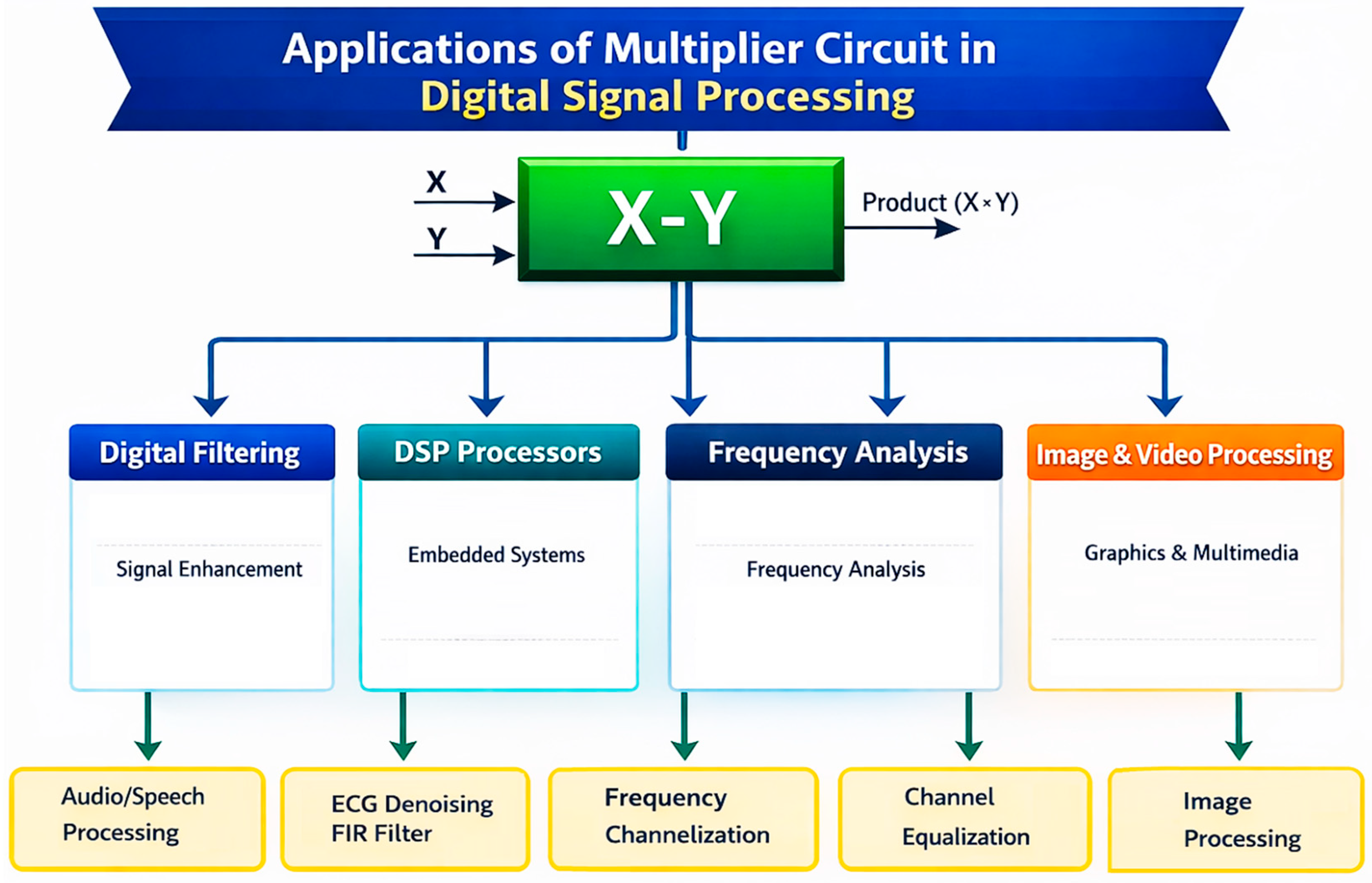
These requirements motivate the development of efficient multiplier architectures with reduced delay and hardware overhead, making compact DTM-based designs a strong candidate for high-throughput nanoscale arithmetic. The general applications of the multiplier for signal processing are illustrated in
Figure 3. In addition, the main processes of digital filtering, frequency analysis and signal enhancement are facilitated through efficient multipliers and find extensive applications in audio/speech processing, biomedical signal denoising and embedded DSP systems. The value also reflects the suitability of multipliers in frequency-domain processing and image and video processing, such as channelization, equalization, and image processing. Since these applications are very dependent on repeated multiply-accumulate operations, tailored multiplier architectures are the only way to get high performance, low latency, and energy-efficient DSP implementations.
Low-latency, low-energy multiplication operations are essential for efficient signal-processing pipelines, including filtering, feature extraction, and classification. In many real-time systems, sampled data are digitized and processed through stages such as preprocessing (e.g., denoising and normalization), feature extraction, and decision-making algorithms, where multipliers are repeatedly used in convolution, correlation, and transforming computations. Therefore, improving multiplier efficiency directly contributes to higher throughput and reduced power consumption in next-generation embedded and nanoscale computing platforms [
4].
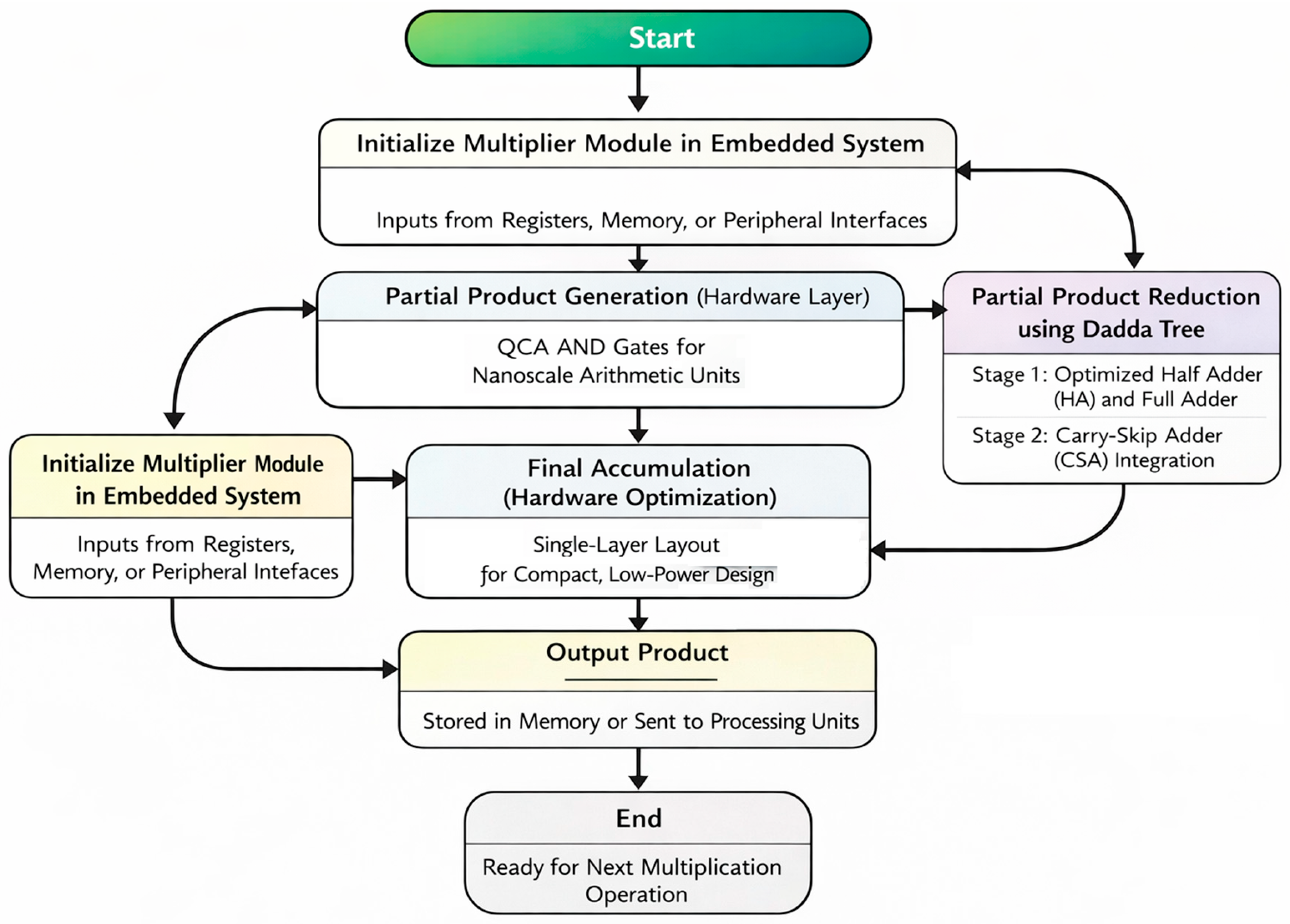
The flow chart illustrated in
Figure 4 demonstrates the end-to-end workings of the proposed QCA-based DTM in embedded hardware and microsystems. It starts with the steps of initializing the multiplier module, and getting input operands in registers, memory or peripheral interfaces. The arithmetic layer of nanoscale is then represented by developing the partial products using QCA AND gates. A Dadda tree is an effective way to minimize these products with optimized HA, FA and CSA in such a way that the propagation and circuit complexity are minimized. The final accumulation is performed in a one-layer format to offer compactness and reduced power consumption to generate the final product of output that can be saved or transmitted to processing units. The flow shows the focus of the proposed framework on high-speed, area-efficient and low-power embedded microsystem multiplication.
3.1. The Full Adder Design
FA is one of the basic components of arithmetic circuits and is common with digital systems [
24], particularly those based on multiplication and accumulation structures [
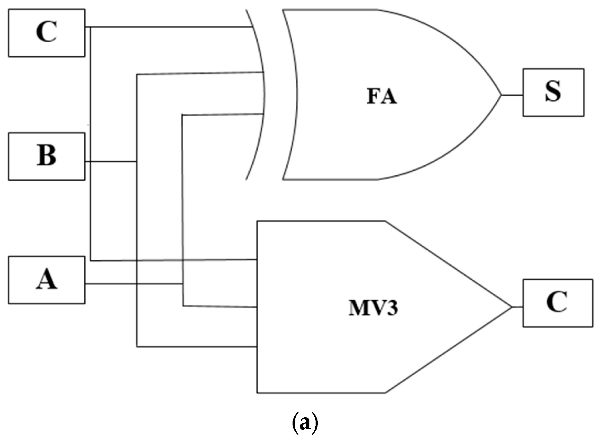
25]. It is a combinational circuit, which calculates the addition of three 1-bit inputs A, B, and C (carry-in) and generates two outputs namely sum and carry [
26]. The behavior of the FA can be described as follows: when any two out of three inputs are logic one and the remaining input is logic one then the carry output will be logic one at the same time as the Sum output will be the odd parity of the inputs. The logical expression of FA is provided in the form of logical expressions in the form of Equations (1) and (2) [
24].
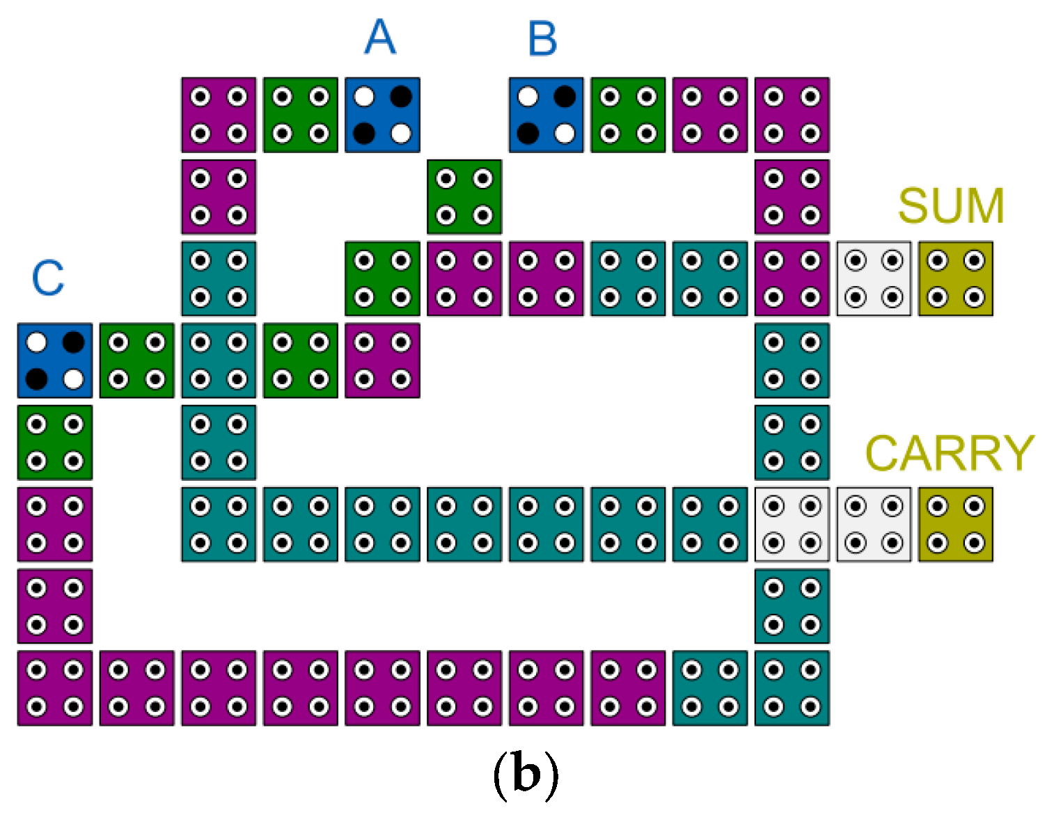
Figure 5(a and b) respectively represent the gate-level representation and the QCA layout [
25].
The implemented FA contains 51 QCA cells and occupies an area of 0.037 μm
2. Its basic logic structure follows the FA reported in [
25]; therefore, this paper does not claim the FA as a completely new primitive. Instead, the FA is used as a compact arithmetic building block and is further adapted at the layout and clocking level to improve its compatibility with the proposed DTM. In particular, minor layout and clock-zone refinements were applied to reduce routing overhead and improve signal propagation balance. Therefore, the contribution of this work is positioned at the multiplier architecture and layout-integration level, supported by an optimized use of the FA block rather than by claiming a fully new FA design.
where
and
are one-bit operands,
is the carry input,
is the parity output,
is the majority output, and
denotes the three-input majority function.
3.2. The Recommended Carry-Skip Adder
A CSA, also referred to as a carry adder bypass, is a type of adder that aims at reducing the time lag in ripple-carry adders [
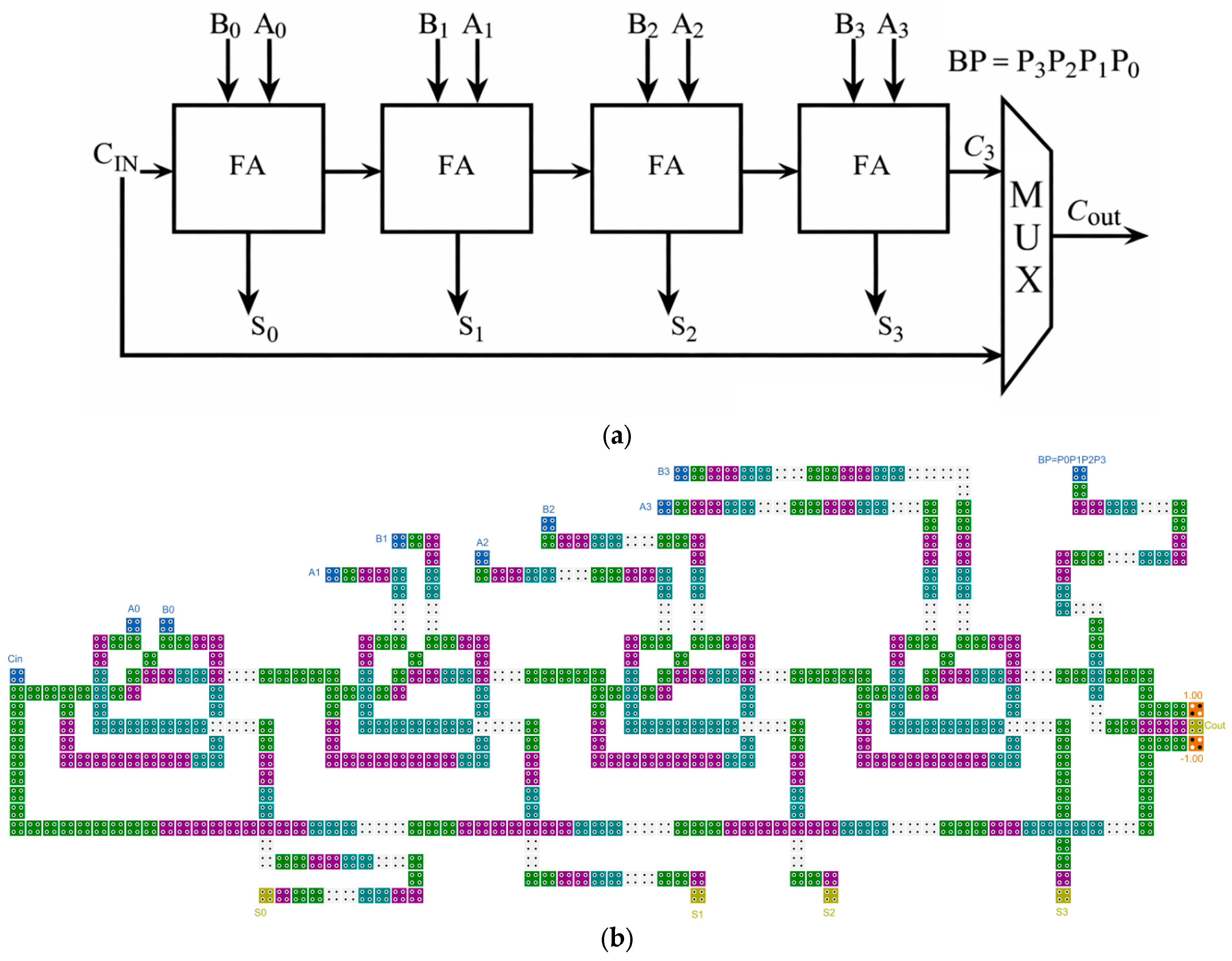
27]. The CSA speeds up the addition process, allowing for skipping the carry through a set of bits. It aims to minimize the time taken to stabilize the carry input and to reach the final value of the output. A CSA with n bits consists of a multiplexer, a chain of n-bit carry-ripple, and an n-input AND gate, as shown in
Figure 6a [
28]. The partial products are added together in an efficient manner within a CSA in DTMs, minimizing the carry propagation delays. This enhances the effectiveness and speed of the multiplier. The architecture of the Dadda tree reduces adders as much as possible, reducing area and power usage over other designs such as Wallace trees. By integrating CSAs at various levels, the multiplier achieves rapid addition and high throughput during multiplication [
29]. Moreover, the suggested QCA-based layout of CSA is depicted in
Figure 6b, which consists of 525 cells occupying an area of 0.74 μm
2 with a delay of 4.5 clock phases.
3.3. The Recommended Dadda Tree Multiplier
An effective hardware solution for multiplying two unsigned integers is the DTM, which was first presented by Luigi Dadda in 1965 [
30]. Moreover, carefully positioning FA and HA in the critical route minimizes the number of stages required to reduce partial products. The Dadda multiplier can be relatively faster than the other multipliers and usually requires less hardware because it uses fewer counters [
31]. However,
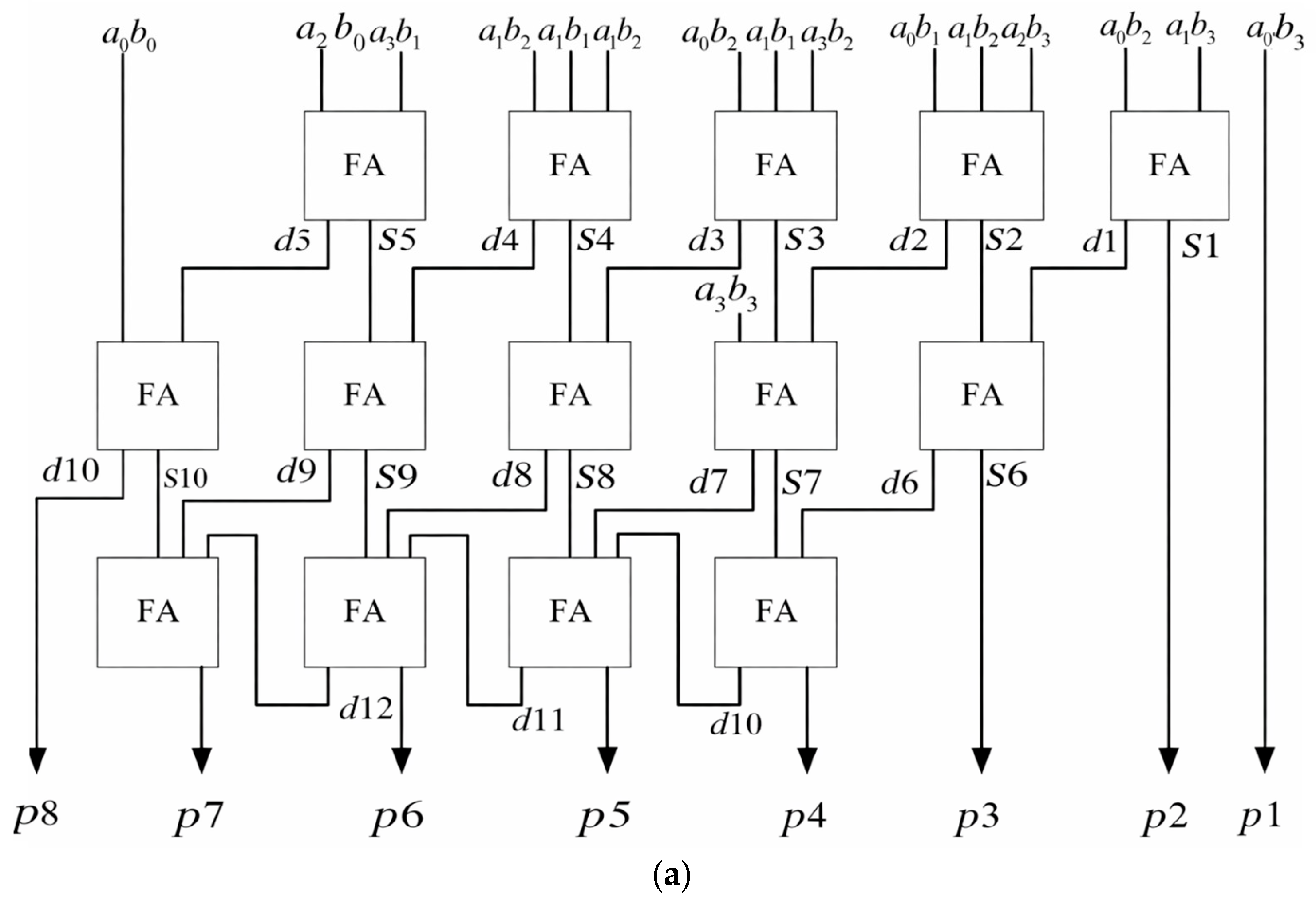
Figure 7a illustrates the architecture of the DTM [
32], and
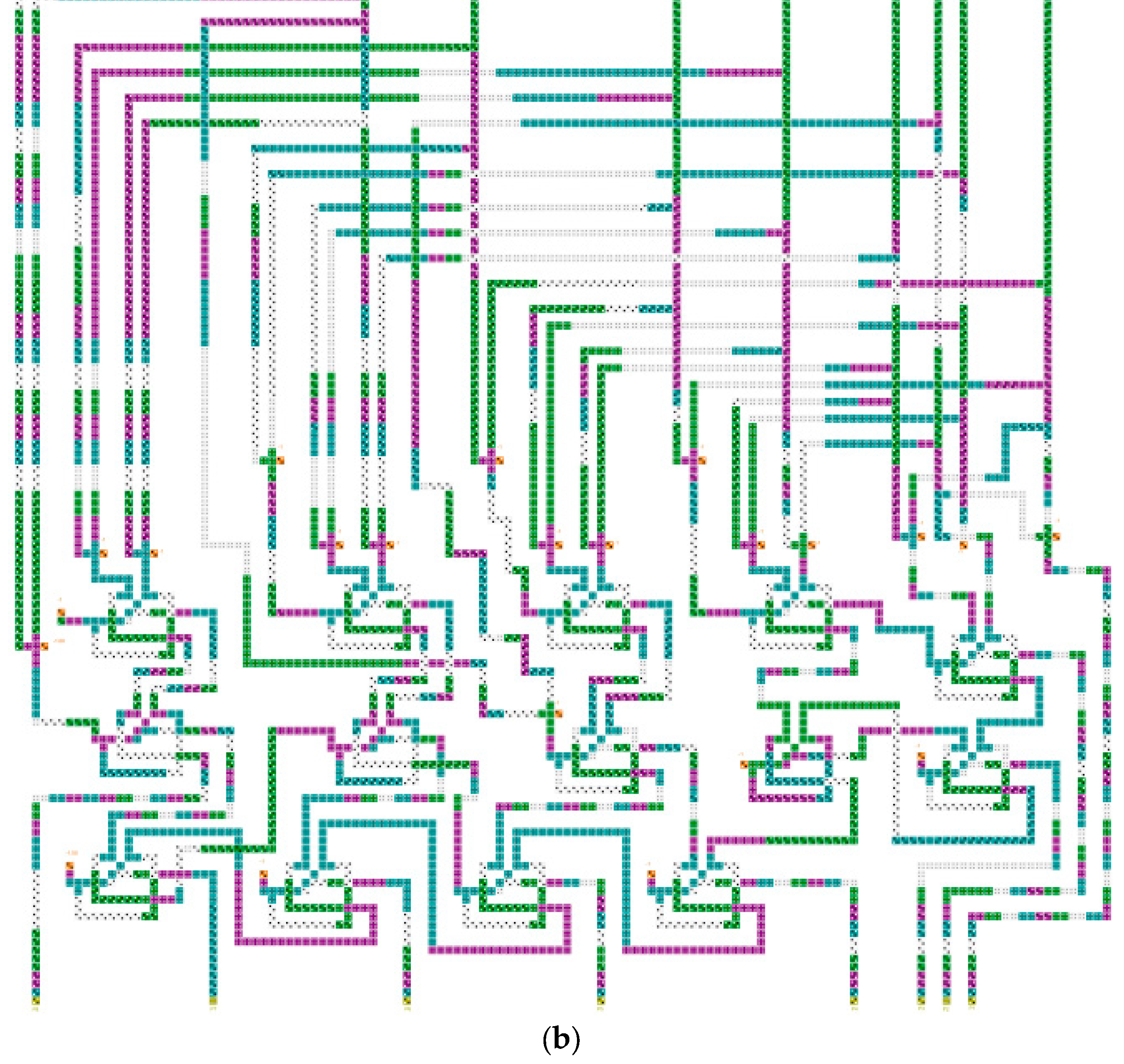
Figure 7b illustrates the QCA-based layout of the DTM which contains 4282 cells with an area of 6.14 μm
2. In the DTM, partial products are minimized to two rows using the minimal number of reduction stages. Moreover, for an N-bit multiplicand and multiplier, the operation generates N × N partial products, which are organized in a matrix. The DTM progressively reduces the matrix height to two rows over a series of reduction stages [
32].
In the Dadda multiplier, the partial-product matrix is reduced according to a predefined sequence of target heights. Starting from the final two-row matrix height
, the next target heights are generated as mentioned in Equation (3):
where
denotes the reduction-level index and
represents the floor operation. Based on this rule, the Dadda height sequence becomes
. For an
multiplier, the largest target height not exceeding the initial partial-product matrix height is selected, and the matrix is progressively compressed through successive reduction stages until only two final rows remain. During compression, full adders and half adders are selectively inserted to ensure that the height of each partial-product column does not exceed the selected Dadda target height. The sum output of each adder remains in the same column for the next reduction stage, whereas the carry output is transferred to the next higher-weight column [
32].
Compared with more aggressive compression schemes, the Dadda multiplier reduces the number of required counters by delaying some reductions until later stages. This strategy can lower hardware complexity and area consumption, although the final accumulation stage remains important because the summation of the last two rows determines the overall propagation delay. Therefore, efficient organization of the final adder and routing structure is essential for achieving a compact and high-performance DTM in QCA.
In addition,
Table 1 explains the major architectural stages of the proposed design flow, including partial-product generation, Dadda reduction scheduling, building-block integration, clock-zone planning, single-layer routing strategy, final accumulation, and verification methodology. The purpose of this explanation is to demonstrate that the proposed work follows a structured architectural optimization methodology rather than a straightforward block-level composition approach. Additionally, it also highlights how each design stage contributes toward compact layout realization, reduced routing overhead, synchronization stability, and scalable nanoscale arithmetic implementation.
3.4. Design Rationale and Cell-Reduction Mechanism
The reduction in cell count and occupied area is achieved through a combination of architectural and layout-level decisions. First, the Dadda reduction strategy minimizes the number of HA and FA elements required at each compression level. Instead of compressing all columns aggressively, the Dadda method delays some reductions and inserts only the adders needed to satisfy the selected target column height. This avoids unnecessary intermediate logic and reduces hardware overhead.
Second, the proposed layout reduces routing cells by placing arithmetic modules close to their corresponding partial-product columns. In QCA circuits, routing cells often contribute significantly to total cell count; therefore, shortening inter-module wires directly reduces the final layout size. Third, the use of a single-layer coplanar organization avoids multilayer crossing overhead and simplifies clock-zone assignment. These factors explain why the proposed DTM reduces cell count and occupied area compared with representative QCA multiplier layouts.
4. Simulation Results
This section presents the simulation environment, verification strategy, functional waveforms, comparative evaluation, and energy/power analysis of the proposed QCA circuits. To address both functional correctness and energy-aware behavior, the proposed circuits were evaluated using QCADesigner 2.0.3 [
33] and QCADesigner-E 2.2 [
34]. QCADesigner 2.0.3 was used for layout-level functional verification, mainly through the Bistable Approximation engine, while QCADesigner-E 2.2 was used for energy-aware analysis using the Coherence Vector with energy engine. Where computationally feasible, the Coherence Vector engine was also considered for polarization-level verification of smaller or representative circuit blocks.
The Bistable Approximation engine provides efficient logic-level validation for large QCA layouts, whereas the Coherence Vector model offers more detailed polarization-level analysis by considering cell interactions more accurately. The Coherence Vector with energy mode in QCADesigner-E further enables the estimation of energy dissipation, power, and PDP under the same QCA modeling assumptions. Therefore, the verification strategy combines functional validation, polarization-level checking, and energy-aware evaluation, as summarized in
Table 2.
Although this multi-mode verification improves the reliability of the simulation analysis, all results remain within the QCADesigner/QCADesigner-E modeling framework. Therefore, the results should not be interpreted as technology-aware validation for molecular QCA, SiDB logic, or other field-coupled nanotechnologies without additional redesign and simulation using platform-specific tools.
Since QCA computation is controlled by clock phases, timing consistency was considered for the main majority-voter and adder branches. In QCA layouts, unequal arrival times at a majority voter can lead to unstable or incorrect evaluations. Therefore, the proposed layout was arranged so that inputs entering the majority-based logic stages reach the evaluation region in compatible clock phases. For the large DTM structure, representative reduction paths and the final accumulation path were checked to confirm the intended clock-zone order. This clock-aware verification is summarized in
Table 3.
This timing check does not replace technology-aware clock-field modeling; rather, it confirms that the proposed QCA layout follows a consistent clock-zone ordering within the QCADesigner/QCADesigner-E simulation framework.
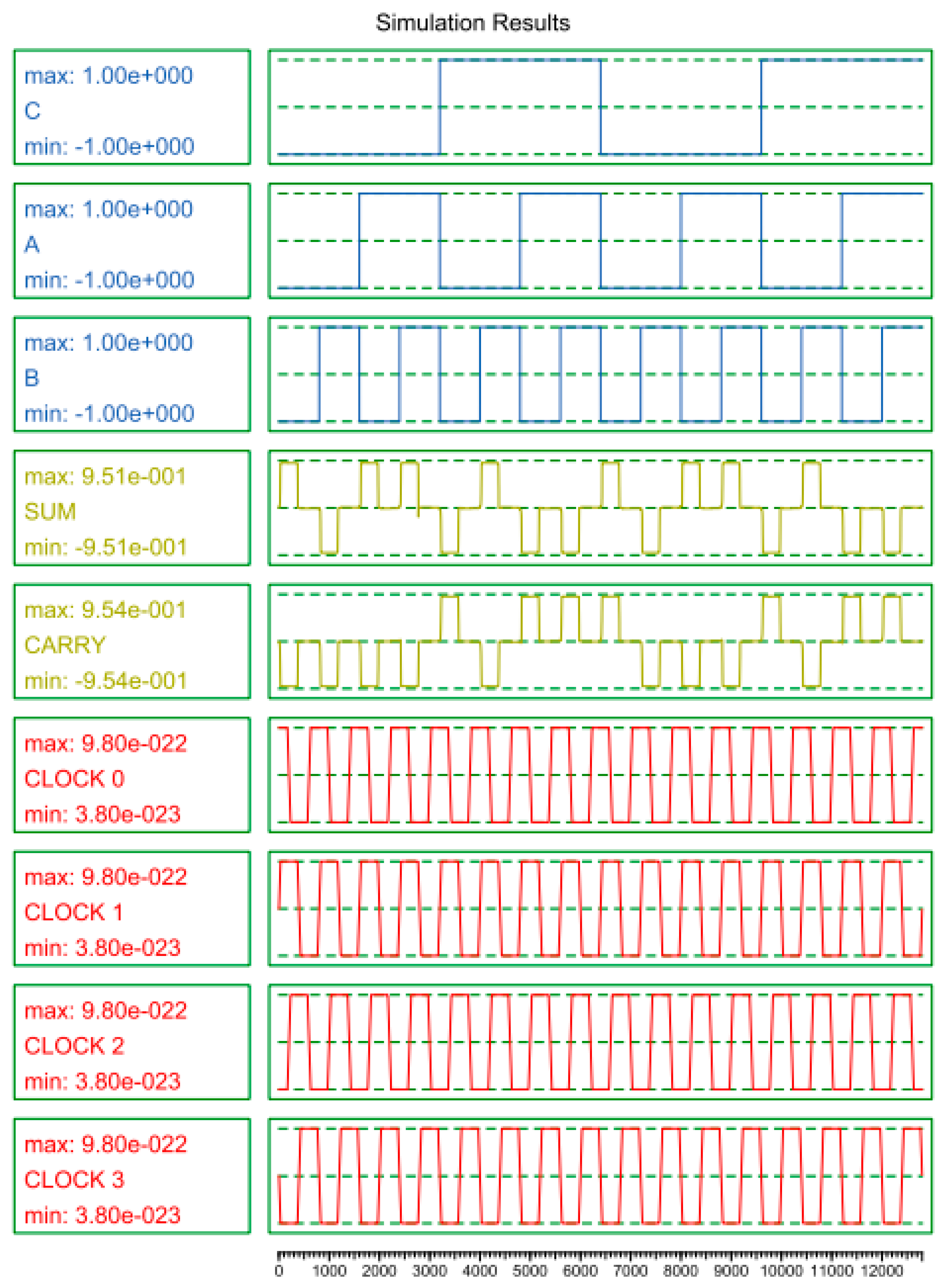
The implemented FA simulated output waveforms are presented in
Figure 8 and exhibit proper sum and carry behavior in all combinations of inputs. The layout characteristics of the FA are reported in
Table 4, and the comparison shows that the implemented coplanar implementation has a compact implementation that can be integrated into more coplanar circuits in larger arithmetic architectures.
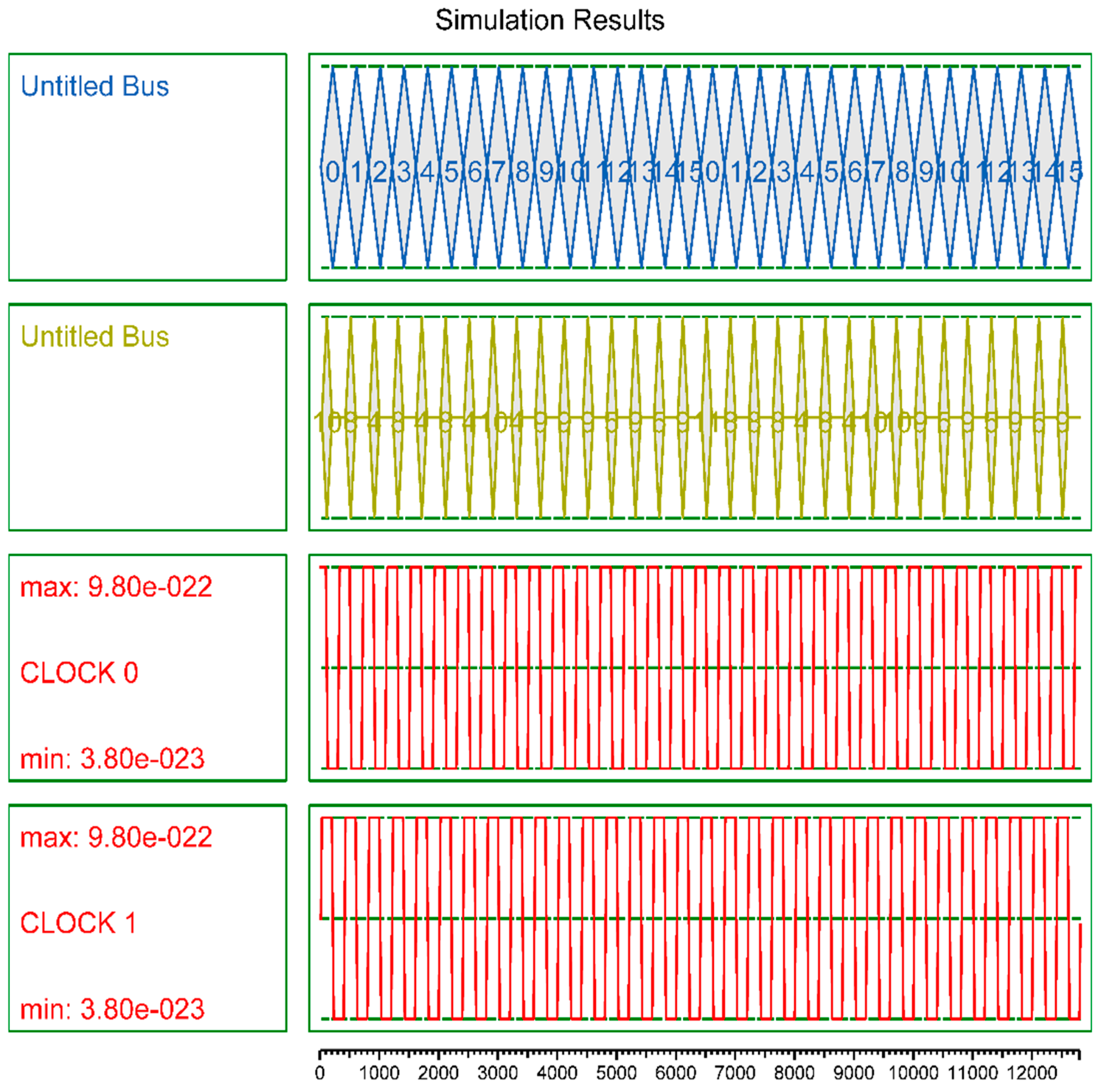
In
Figure 9, the simulated waveform of the suggested CSA is shown. The waveform colors correspond to the standard display format of the simulation software, where the labeled traces represent the corresponding input, output, and clock signals.
Furthermore, as reported in
Table 4, the proposed structure demonstrates measurable reductions in cell count and occupied area compared with the reference design [
35], indicating improved layout efficiency. The implemented FA consists of 51 cells and occupies 0.037 μm
2. The design follows a coplanar (single-layer) layout approach, which avoids multi-layer routing and reduces wire-crossing overhead; consequently, it provides a practical path toward higher clocking feasibility and more scalable QCA arithmetic blocks.
The proposed QCA-based DTM is mainly optimized for reducing cell count, occupied area, and layout complexity. Therefore, the comparison emphasizes area-oriented efficiency while also reporting clocking latency to show the resulting tradeoff.
In comparison with the earlier reported designs, the proposed DTM shows improvements of ~84%, ~93%, and ~69% in terms of cell count, area, and clocking when compared to Design #01 in [
21]. A similar trend is observed for Design #02 in [
21], where the proposed DTM also achieves substantial reductions in cell count, occupied area, and clocking latency.
Table 4.
Comparison table of proposed designs with previous designs.
Table 4.
Comparison table of proposed designs with previous designs.
| Designs | In | Cells | Area (μm2) | Clocking |
|---|
| FA | [36] | 145 | 0.162 | 1.25 |
| [37] | 105 | 0.172 | 1.25 |
| [38] | 102 | 0.0971 | 2 |
| [39] | 95 | 0.098 | 1.5 |
| [35] | 73 | 0.044 | 0.75 |
| Proposed Design | 51 | 0.037 | 1 |
| CSA | [33] | 815 | 0.738 | 4 |
| [17] | 698 | 0.618 | 4 |
| [18] | 665 | 0.65 | 2.5 |
| [19] | 696 | 0.66 | 2.5 |
| Proposed Design | 525 | 0.74 | 4.5 |
| DTM | [21] Design #01 | 26,973 | 82.19 | 38 |
| [21] Design #02 | 26,499 | 82.18 | 36 |
| [20] | 10,475 | 10.2 | 10.25 |
| Proposed Design | 4282 | 6.14 | 11.75 |
Compared with representative QCA multiplier baselines, the proposed DTM achieves substantial reductions in cell count and occupied area. However, the latency improvement is not universal. In comparison with [
20], the proposed design reduces cell count and area, but its clocking latency increases from 10.25 to 11.75 clock cycles. Therefore, the main advantage of the proposed architecture is area efficiency and layout compactness rather than absolute latency minimization. This confirms that the proposed design provides an area-oriented tradeoff suitable for compact nanoscale arithmetic layouts.
4.1. Technology Scope and Interpretation of Area/Energy Metrics
The present work is based on the conventional QCADesigner/QCADesigner-E circuit abstraction, where each QCA cell follows the standard four-dot/two-electron model and layout metrics are extracted under the simulator’s default geometric assumptions. Therefore, the reported occupied area should be interpreted as a layout-level area within this simulation model, not as a universal fabricated area valid for all QCA implementations. Similarly, the reported energy and power values are simulator-based estimates and are intended for comparative evaluation among layouts modeled under the same assumptions.
Recent molecular field-coupling nanocomputing studies have shown that technology-aware modeling is essential when moving from generic QCA layouts to molecular implementations. In particular, Ardesi et al. [
40] emphasized that general QCA simulation tools approximate molecular systems as ideal quantum-dot systems and cannot fully capture effective molecular behavior. Therefore, technology-aware approaches such as SCERPA and ToPoliNano are needed for molecular FCN validation. In this work, the proposed DTM is not claimed as a molecular-FCN-ready layout; rather, it is presented as a layout-level QCA arithmetic architecture evaluated under the QCADesigner/QCADesigner-E framework [
34].
We do not claim that the proposed layout can be directly transferred to molecular QCA, silicon dangling-bond logic, nanomagnetic logic, or other field-coupled nanocomputing platforms without redesign. These technologies require technology-specific cell models, spacing rules, clocking schemes, electrostatic models, and validation tools. Accordingly, future work should include technology-aware redesign and validation using platform-specific tools such as SCERPA/ToPoliNano, SiQAD, QuickSim, or related FCN simulation frameworks.
4.2. Power Analysis
Power analysis in QCA differs fundamentally from conventional CMOS circuits because QCA switching does not rely on a continuous flow of current. Instead, computation is realized through Coulombic interactions and controlled polarization switching of electrons confined in quantum dots; therefore, energy dissipation is primarily governed by cell polarization transitions and the applied clocking mechanism [
41]. In this study, the energy characteristics of all QCA-based architectures are evaluated using QCADesigner-E [
34]. The corresponding energy dissipation results for the designs examined are summarized in
Table 5.
Another important parameter is the kink energy (Ek), which represents the electrostatic interaction energy between neighboring cells and directly impacts switching behavior and reliability. To this end, power analysis is often presented at different normalized operating points (e.g., 0.5 Ek, 1 Ek, and 1.5 Ek) to investigate the behavior of a circuit at varying strengths of interaction and operating conditions [
34,
42]. QCADesigner-E can allow the estimation of energy dissipation by modeling polarization switching dynamics, clock energy and intercellular interactions and offers a useful framework in comparative energy evaluation of QCA circuits [
34].
However, as well as energy dissipation,
Table 5 records the cost metric of the proposed circuits, such as Cost = Area × Latency
2. In addition, the PDP is obtained as a measure of the total energy-speed tradeoff. In line with custom, a hypothetical frequency of 1 THz is adopted in converting energy measures to a power value, and PDP is calculated as PDP = Power × Delay [
43].
4.3. Temperature Effect on QCA Designs Analysis
One important parameter that controls the stability and proper functioning of QCA circuits is temperature since sound computation requires consistent cell polarization states. When the temperature rises, the stochastic variation with thermal agitation decreases the average polarization of the output (AOP), which, in turn, decreases signal integrity and can cause inaccurate logic interpretation at the output. This degradation is further enhanced in layouts that have weaker intercellular Coulombic coupling in which the polarization structure can readily be disturbed by thermal energy and generated perturbations to the originally desired localization of the electrons [
44]. The fact that polarization is dependent on temperature can be explained through a Boltzmann-type relationship, as in Equation (4) [
44]:
where
denotes the polarization of the ground state,
E the effective energy barrier between polarization states,
is the Boltzmann constant and
T the absolute temperature. By this expression, an increase in
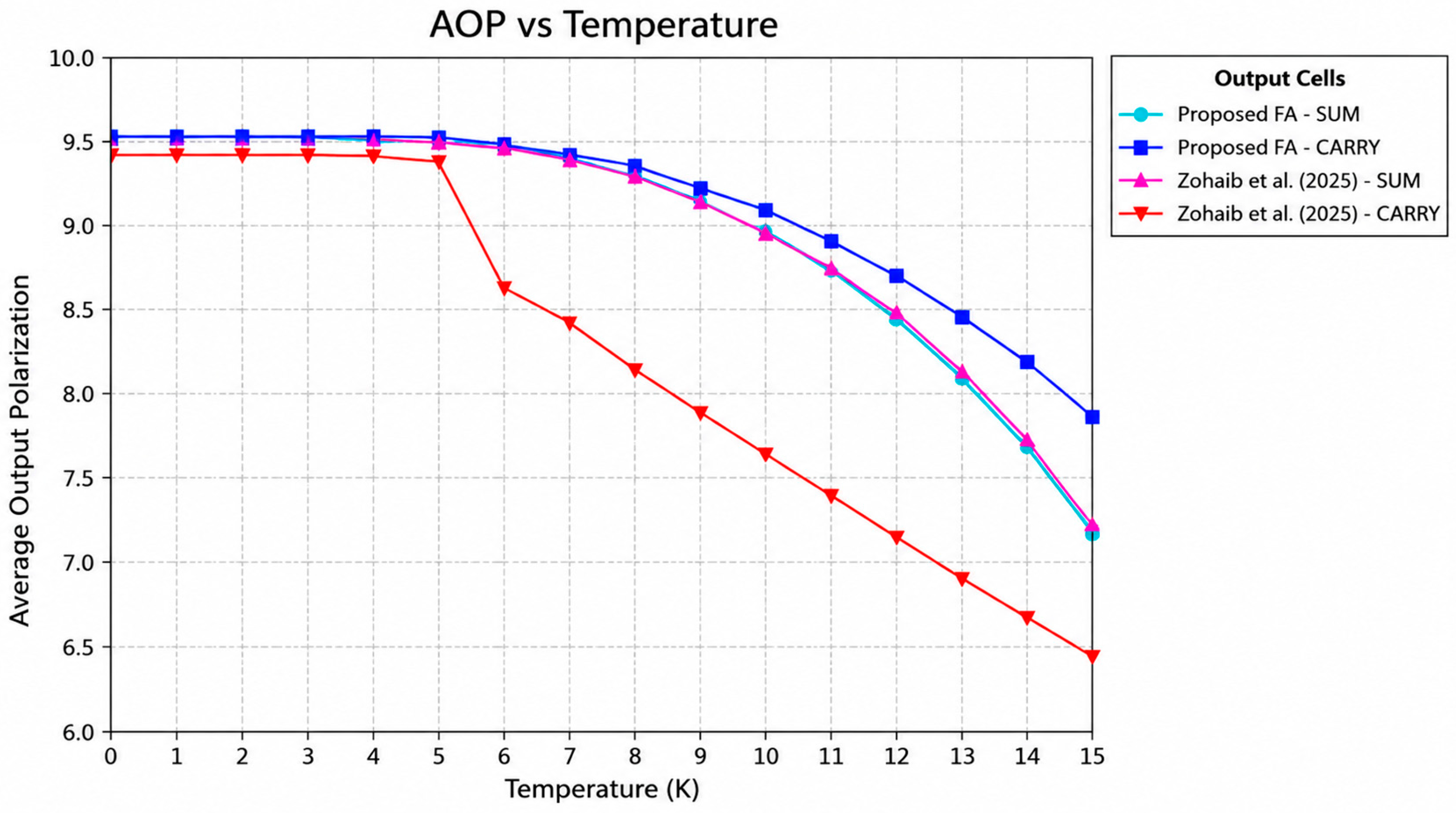
T decreases the exponent factor hence the progressively exponential decrease in the magnitude of polarization. The temperature sensitivity of the proposed QCA-based FA can be plotted in
Figure 10 by drawing the AOP versus temperature. As can be seen, the AOP is slowly decreasing as temperature increases, which implies that polarization fidelity diminishes and thus the critical role of robust cell-to-cell interactions and layout stability.
As shown in
Table 6, the average output polarization (AOP) decreases monotonically as temperature increases for both the proposed FA and the reference FA [
25]. This behavior is expected because higher temperature increases thermal agitation, which weakens polarization stability and reduces the reliability margin of QCA outputs. At low temperatures between 0 K and 5 K, both SUM and CARRY outputs remain highly polarized, with AOP values close to 9.4–9.5, indicating stable operation in the low-temperature range. As the temperature increases beyond 10 K, the polarization degradation becomes more evident, particularly in the CARRY output.
The proposed FA shows a clear advantage over FA [
25] in the CARRY path at elevated temperatures. For example, at 10 K, the proposed CARRY output achieves an AOP of 9.06, compared with 7.61 for FA [
25], corresponding to an improvement of 1.45. At 12 K, the proposed design reaches 8.64, while FA [
25] reaches 7.11, giving an improvement of 1.53. Similarly, at 14 K and 15 K, the proposed CARRY output remains higher, with values of 8.12 and 7.83, compared with 6.64 and 6.42 for FA [
25], respectively.
These results indicate that the main improvement of the proposed layout is concentrated in the carry-generation/propagation path, which is usually more sensitive to weak coupling, routing complexity, and thermal effects. In contrast, the SUM outputs of both designs remain very close across the full temperature range. Overall, the proposed FA provides better thermal tolerance and larger polarization margins, especially for the CARRY output, which can improve the reliability of QCA arithmetic circuits under higher-temperature operating conditions.
4.4. Possible Applications and Relation to Quantum Computing
The proposed QCA-based DTM is primarily intended for nanoscale classical arithmetic rather than direct gate-model quantum computing. Its possible applications include multiply–accumulate units, FIR filtering, transform computation, image/video processing, embedded sensor processing, and compact arithmetic data paths for post-CMOS nanoscale systems. In these workloads, multiplication is repeatedly used; therefore, reducing multiplier area and routing complexity can improve the feasibility of compact low-power arithmetic hardware.
It is also important to distinguish QCA-based computing from gate-model quantum computing and quantum-information protocols. Recent quantum-computing and quantum-information studies, such as quantum generative models based on quantum convolutional neural networks and semi-quantum private-comparison protocols using high-dimensional entangled states, rely on qubits, quantum states, quantum communication resources, and protocol-level learning or security analysis [
45,
46,
47]. In contrast, the proposed QCA multiplier performs classical Boolean arithmetic through field-coupled cell polarization and does not execute quantum algorithms or quantum communication protocols directly. Therefore, its possible connection to quantum-computing systems is indirect, for example as a compact low-power classical support circuit for preprocessing, postprocessing, or control/interface electronics in future hybrid classical–quantum platforms.
4.5. Limitations of the Proposed Design
Although the proposed QCA-based DTM achieves compact cell count and occupied area, several limitations should be acknowledged. First, the study is based on layout-level simulation using QCADesigner/QCADesigner-E, and no fabricated implementation is provided. Therefore, the reported area, energy, power, and PDP values should be interpreted as simulation-based estimates rather than experimental measurements.
Second, the design is optimized mainly for area and cell-count reduction. Although the latency is competitive, it is not lower than all previously reported QCA multiplier designs. Third, the current implementation is demonstrated for a fixed multiplier size; larger word sizes may introduce additional routing, synchronization, and clock-zone challenges. Fourth, the current validation does not fully include fabrication-level non-idealities such as cell displacement, missing cells, process variation, or technology-specific constraints. Future work should address defect-tolerant analysis, technology-aware simulation, and CAD-assisted placement/routing optimization.
5. Conclusions and Future Works
This paper presented a QCA-based DTM aimed at compact and energy-aware nanoscale multiplication for real-time, high-throughput computing workloads designed for nanoscale embedded hardware and microsystems. The design was implemented and verified using QCADesigner 2.0.3, and the proposed DTM achieves a compact realization of 4282 cells within 6.14 μm2. The proposed architecture uses less cell area by factors of about 59% and less cell utilization by factors of about 40% than a recent compact QCA multiplier baseline, showing a much better area density tradeoff, and has a small increase in clocking latency. In general, the findings validate that layout-conscious optimization of architecture can greatly improve the feasibility of QCA multipliers as scalable design units of next-generation nanoscale arithmetic units and signal-processing accelerators with severe energy and area limitations. To enhance the proposed framework in future work, various outlines can be used to augment it. To achieve better latency scalability in multipliers with large word sizes, first, it is possible to extend the architecture by adding larger word sizes and researching ways to clock-sensitively reduce area, and second, it is possible to improve scalability by adding word-size independence in the extension of the point-to-point architecture. Second, some non-ideal operating conditions can be made more robust by adding defect-conscious and temperature-conscious optimization (e.g., cell omission tolerance and polarization-margin improvement). Third, routing, clock-zone assignment and module placement can all be optimized to minimize wire crossings and critical paths and energy behavior can be further enhanced by applying automated synthesis and evolutionary optimization methods to co-optimize routing, clock-zone assignment and module placement. Finally, validating the proposed multiplier within broader nanoscale data paths (e.g., MAC units, FIR kernels, and transform blocks) will provide a clearer system-level perspective on throughput, reliability, and energy efficiency in next-generation nano-computing platforms.