Article

Implementation of a Programmable Electronic Load for Equipment Testing

by
León Felipe Serna-Motoya
,
José R. Ortiz-Castrillón
,
Paula Andrea Gil-Vargas
,
Nicolás Muñoz-Galeano
,
Juan Bernardo Cano-Quintero
and
Jesús M. López-Lezama
*
Research Group on Efficient Energy Management (GIMEL), Departamento de Ingeniería Eléctrica, Universidad de Antioquia (UdeA), Calle 70 No. 52-21, Medellín 050010, Colombia
*
Author to whom correspondence should be addressed.
Computers 2022, 11(7), 106; https://doi.org/10.3390/computers11070106
Submission received: 18 May 2022 / Revised: 10 June 2022 / Accepted: 21 June 2022 / Published: 28 June 2022
(This article belongs to the Special Issue Computing, Electrical and Industrial Systems 2022)

Abstract

:
This paper presents the implementation of an AC three-phase programmable electronic load (PEL) that emulates load profiles and can be used for testing equipment in microgrids (MGs). The implemented PEL topology is built with a voltage source inverter (VSI) which works as a current controlled source and a Buck converter which permits the dissipation of active power excess. The PEL operation modes according to the interchange of active and reactive power and its operation in four quadrants were determined. The power and current limits which establish the control limitations were also obtained. Three control loops were implemented to independently regulate active and reactive power and ensure energy balance in the system. The main contribution of this paper is the presentation a detailed analysis regarding hardware limitations and the operation of the VSI and Buck converter working together. The PEL was implemented for a power of 1.8 kVA. Several experimental results were carried out with inductive, capacitive, and resistive scenarios to validate the proper operation of the PEL. Experimental tests showed the correct behavior of the AC three-phase currents, VSI input voltage, and Buck converter output voltage of the PEL for profile changes, including transient response.

1. Introduction

Non-conventional renewable energy sources (NCRESs) and their installation in MGs are part of a global trend toward clean and sustainable electricity generation. This brings challenges in terms of stability, generation, interconnection and control to allow these systems to connect and operate properly together with conventional electricity generation systems. NCRES such as solar and wind depend on several factors such as temperature, irradiance, and wind speed; in consequence, NCRESs are volatile and depend on the time, day, and season of the year (weather conditions). Therefore, the correct design of an MG implies a detailed sizing, considering safety and continuity of service as a priority [1]. For this reason, it is important to verify the correct operation of all devices that compose the MG before its connection, in order to guarantee a correct synchronization, operation, and communication.
A PEL is a power electronics device that allows for the testing of equipment and NCRESs in MGs [2]. It emulates several load or source profiles such as transient and steady-state operation for equipment under test (EUT) [3,4,5]. This is done to assess the performance of a single or several devices working jointly within an MG. A PEL can be seen as a regulated current source, the control system of which regulates the current to emulate the desired load or NCRES profiles. There are two PEL types: unidirectional and bidirectional. Unidirectional PELs can be further classified in two categories: the first one only consumes energy from the power grid and can be related with residential, commercial, or industrial end users that may have linear loads (such as household appliances and motors) and non-linear loads (such as computers and illumination). This PEL type is able to modify the power factor and waveform of the current for emulating loads that introduce harmonics to the grid. The second unidirectional PEL emulates distributed generators (DGs) that only inject power to the electrical grid, such as solar and eolic generators [6,7,8,9,10,11,12]. Bidirectional PELs are able to emulate load or power sources. This type of PEL features functions for energy consumption and injection depending on its operation mode, which includes storage energy systems (batteries), chargers for batteries from electric vehicles, inverters, converters, and solar panels.
Several topologies of PELs can be found in the scientific literature (single-phase, three-phase, and DC) [3,4,5,13,14,15,16,17,18,19,20,21] from conventional topologies based on variable resistances [7] up to topologies based on joint operation of converters and inverters (such as boost, Buck-boost, back to back, and multilevel) [3,7,21]. The most common PEL applications in MG for testing equipment are storage systems, uninterruptible power supplies, measurement, converters, and inverters (voltage source inverter, VSI) [6,19,22]. PELs have limited functions and different control strategies according to the EUT. For example, a PEL based on a DC/DC Buck-boost converter allows for emulating loads as battery storage systems. This topology is able to consume or inject energy into DC systems. In the same way, back-to-back topology has two emulation modes (consumer and generator) for equipment in AC [3,6,13,22,23,24,25,26,27,28].
In the technical literature, PEL topologies with VSI integrated with Buck converters are reported in [19,29,30]. In [29], a PEL is simulated in PSIM with its model and control scheme. In [19], single-phase and three-phase PEL topologies are simulated, developing several control schemes to emulate different load profiles. In these studies, the real implementation of the power electronics equipment was not performed; the authors only present simulation results and the performance of the PEL was only evaluated in a steady state. In [30], the implementation of a PEL is reported; in this paper, equations for the sizing of the system components and filters were presented. However, the model is not addressed in depth, and neither is the exploration of the operational limits of the PEL. It is worth mentioning that the operational quadrants of the PEL were not taken into account in the aforementioned publications.
This paper presents the implementation of a PEL that can be used for testing equipment in MGs, the maximum active power of which is 1.8 kW . The PEL was developed by the integration of two topologies. The first of these is an inverter (three legs, four wires) to emulate three-phase load profiles, and the second of these is a DC/DC Buck converter to control the DC bus and dissipate the excess of power energy into a resistive element. The main advantage of this implementation lies in its reduced cost with respect to commercially available alternatives. The deduction of the four operating modes is detailed according to the interchange of active and reactive power with the grid. Power and current limits are obtained according to hardware limitations, so it is possible to avoid the malfunctioning of the PEL in its operation. Three control loops are proposed for regulating active and reactive powers, which at the same time ensures the energy balance of the system.
PELs are necessary devices for the performance of tests in MGs in order to verify the adequate behavior of all equipment before their connection with the electrical power grid. For this reason, this paper presents the implementation of a PEL for testing equipment in MGs. This document is organized as follows. In Section 1, the state of the art regarding PEL types and main applications in MGs is presented, showing the PELs’ importance for MGs. In Section 2, the operation principle of a PEL is detailed according to its operation quadrants. Section 3 presents the PEL topology built in this paper. Section 4 presents the control scheme for the developed PEL. In Section 5, the developed PEL is detailed together with its experimental tests. Finally, the most relevant conclusions are presented in Section 6.

2. PEL Operation Modes and Limits

This section presents the operational principle of a PEL connected to the electrical grid based on the energy interchange between two sources (see Figure 1). The PEL is modeled as a voltage source ( V P E L ) in series with an inductor (L), whereas the electrical grid ( V G ) (EUT for this case) operates as another energy source. The magnitude and phase of the current (I) that flows in the circuit directly depends on the voltage difference between V P E L , V G , and the grid impedance ( Z = j ω L ). This allows us to make a first current approach that is represented by using Equation (1). If the electrical grid is used as an angle reference, it is possible to obtain a desired current, modifying the magnitude and phase of V P E L :
I = V G V P E L Z .
PELs are current source devices that permit the emulation of load profiles. In this case, the reference current I = | I | θ I corresponds to the desired current that permits the emulation of different load profiles. Equation (2) relates the AC voltage and the current in the PEL AC terminals ( V P E L = | V P E L | θ P E L ), which are obtained from Equation (1), where θ P E L is the PEL phase voltage angle respective to the angle of V G . Grid voltage is defined as V G = | V G | θ G with θ G = 0 ° , because the electrical grid is the system reference
V P E L = V G Z I .
Figure 2 illustrates the phasor diagrams of I and V P E L . These are depicted as keeping the magnitude of I constant and varying θ I between 0 ° and 360 ° . The circumferences represent the paths for each phasor where the coordinate origin is the tail for each phasor. The left circumference (the smallest one) represents the set of phasors for I. Its center is the origin of the complex plane with a real axis (abscissa) and an imaginary axis (ordinate). The right circumference represents the set of phasors for V P E L , where its center corresponds to the value of ( V G ). Both circumferences are related by Equation (2). Each circumference has its four quadrants (I, II, III, IV) with dotted and colored lines; this representation allows us to see the relationship between the set of phasors I and V P E L . Each group of current phasors (colored and numbered) is related to the corresponding group of voltage phasors having the same numbering and the same color. This relationship is established by Equation (2). This relationship is due to V Z , which is the coupling impedance voltage required to complete Kirchhoff’s voltage law.
Figure 3 presents the operational modes of the PEL developed in this paper. Note that the amplitude of I is constant, varying its phase in the four quadrants ( 0 ° θ I < 360 ° ) with steps of 45 ° . Figure 3a illustrates the beginning of the phasor path ( θ I = 0 ° ) and Figure 3i illustrates its end ( θ I = 360 ° ). The blue phasor corresponds to the reference of the grid voltage or angular reference ( V r e f = V G = | V G | 0 ° ). The black phasor corresponds to the impedance voltage Z ( V Z = | V Z | θ Z ). The green phasor is the PEL voltage ( V P E L = | V P E L | θ P E L ). Finally, the red phasor is the current ( I = | I | θ I ). In this case, Z is an inductive reactance; hence, the current I has a phase of 90 ° in lagging with respect to V Z ( θ Z θ I = 90 ° ). The purpose of this figure is to show how V P E L must behave (in magnitude and angle) in order to obtain a desired current and analyzes when the PEL acts as a load or source, and as inductive or capacitive. The paths of the current and voltages allow us to conclude the following. (1) If the current moves in quadrants I and IV, the PEL behaves as a load. On the contrary, for the current in quadrants II and III, the PEL behaves as a source. (2) The current in quadrants I and II is lagging, whereas the current in quadrants III and IV is leading. Therefore, there are eight operation modes for the PEL:
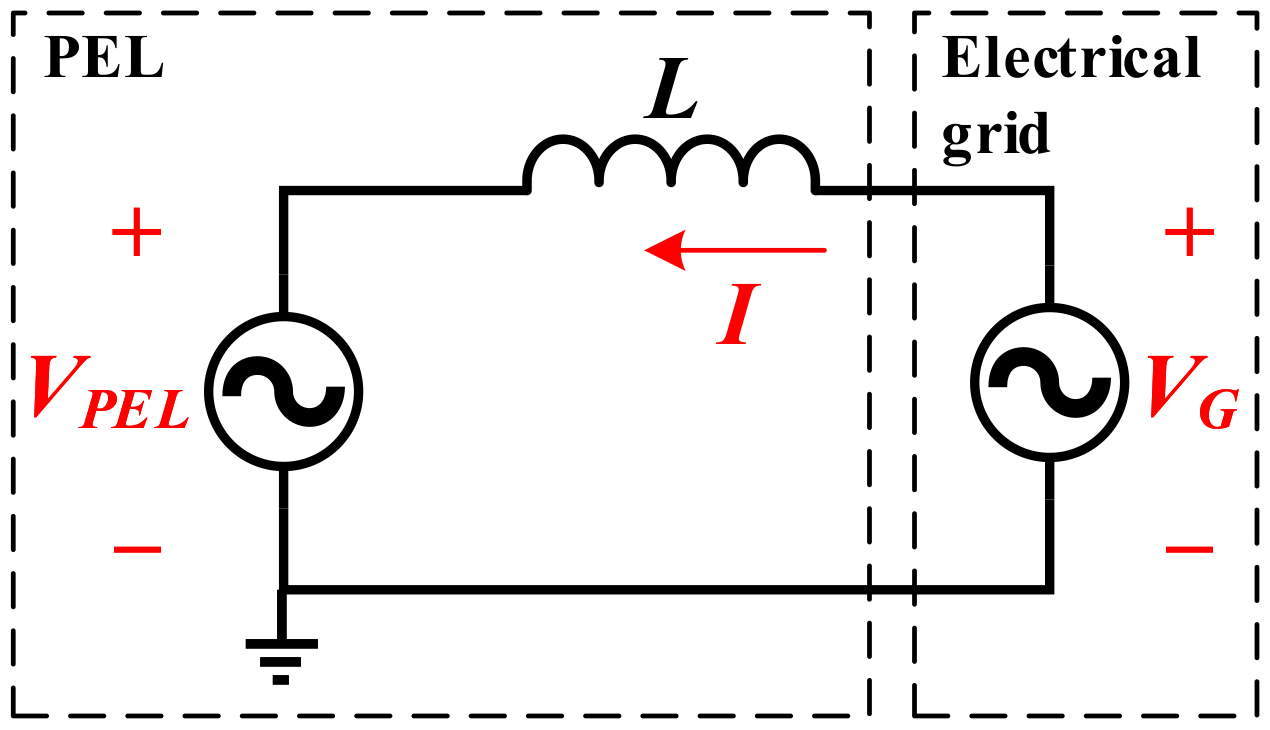
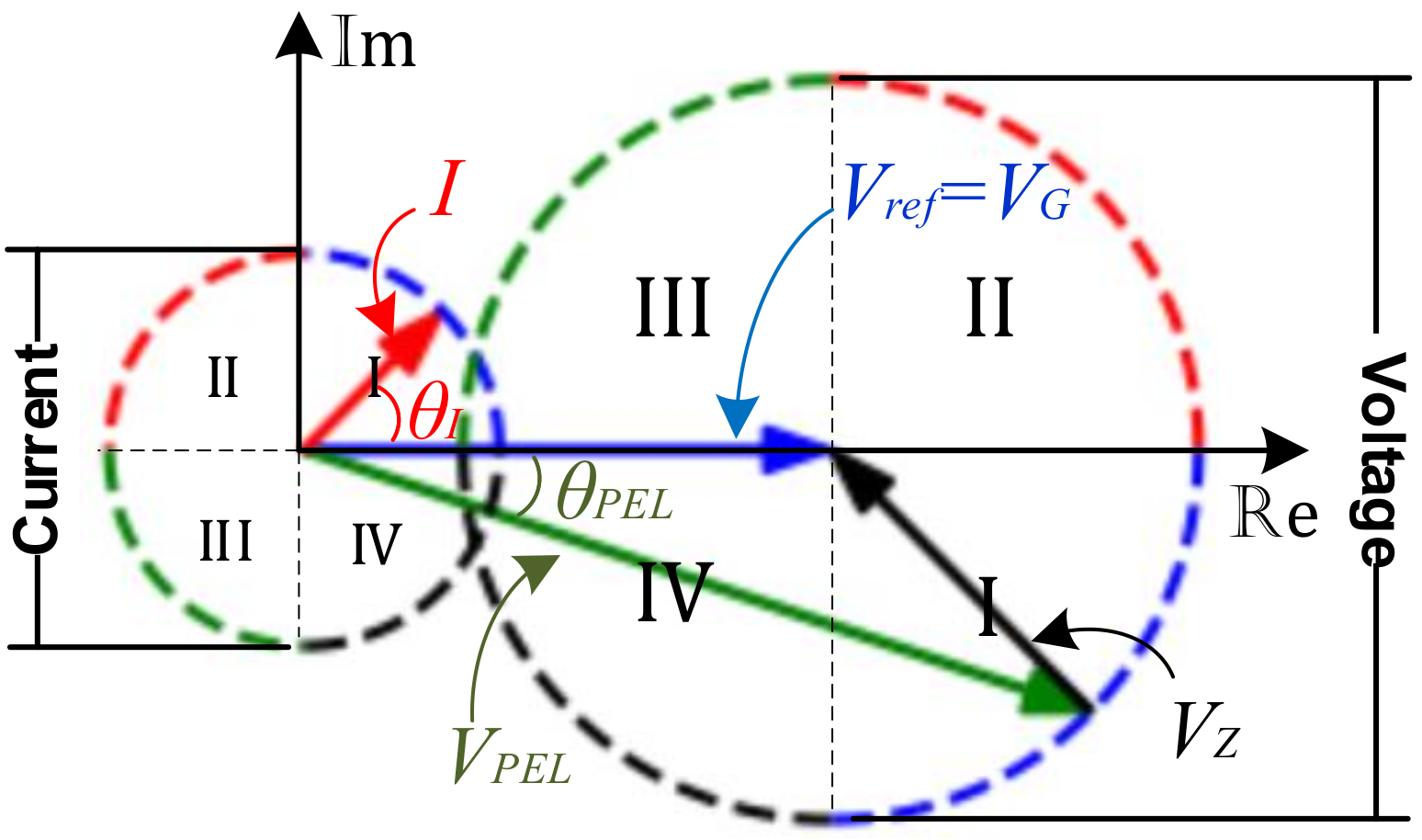
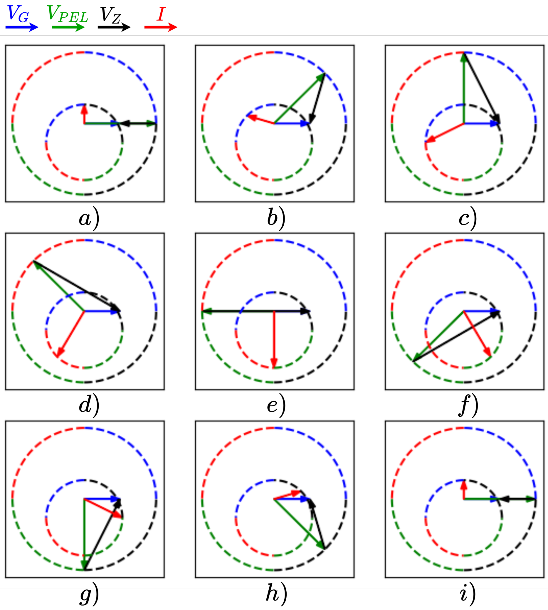
  • Figure 3a,i, PEL as pure resistive load. PEL only consumes active power and its current has the same phase and direction as the electrical grid ( θ I = 0 ° ).
  • Figure 3b, PEL as load resistive–capacitive ( R C ). If desired, a current in the first quadrant ( 0 ° < θ I < 90 ° ), then V P E L should move for the first quadrant of voltage circumference (both are shown with blue dotted lines).
  • Figure 3c, PEL as capacitive load. PEL only consumes reactive power and the current is θ I = 90 ° leading wih respect to the electrical grid.
  • Figure 3d, PEL as leading source. If a current in the second quadrant is desired ( 90 ° < θ I < 180 ° ), then V P E L should move for the second quadrant of voltage circumference (both are shown with red dotted lines).
  • Figure 3e, PEL as pure active source. PEL only injects active power and its current has a phase and direction in opposition to the electrical grid ( θ I = 180 ° ).
  • Figure 3f, PEL as lagging source. If a current in the third quadrant is desired ( 180 ° < θ I < 270 ° ), then V P E L should move for the third quadrant of voltage circumference (both are shown with green dotted lines).
  • Figure 3g, PEL as pure lagging source. PEL only injects reactive power and the current is θ I = 90 ° lagging with respect to the electrical grid.
  • Figure 3h, PEL as resistive–inductive load ( R L ). If desired, a current in the fourth quadrant ( 270 ° < θ I < 360 ° ), then V P E L should move for the four quadrant of voltage circumference (both are shown with black dotted lines).
Figure 3. Operation modes of the PEL: | I | = | I m a x | with 0 ° θ I < 360 ° . (a) pure resistive load, (b) resistive-capacitive load, (c) capacitive load, (d) leading source, (e) pure active source, (f) lagging source, (g) pure lagging source, (h) resistive-inductive load, (i) pure resistive load.
Computers 11 00106 g003
Figure 4 also illustrates the PEL operation mode in its four quadrants. However, the PEL voltage amplitude is constant and greater than the grid voltage amplitude. The purpose of this figure is to show how the current behaves when the PEL voltage is constant and its angle varies ( 0 ° θ P E L < 360 ° ). Figure 4a illustrates θ P E L = 0 ° whereas Figure 4i illustrates θ P E L = 360 ° . In this operation, point θ P E L = θ G = 0 ° ; hence, the current amplitude is at minimum due to the lowest difference of the potential in Z. By varying the angle of the PEL ( 0 ° < θ P E L < 180 ° ) (Figure 4a–d), the current increases its magnitude, obtaining its maximum value in θ P E L = 180 ° (Figure 4e) when V P E L has the opposite direction of V G and the potential difference is at maximum in Z. On the other hand, when the PEL voltage varies between 180 ° < θ P E L < 360 ° , the amplitude of the current decreases (Figure 4f–h), obtaining its minimum value in θ P E L = 360 ° = 0 ° (Figure 4i).
PELs in AC are power electronics devices built with inverters (single-phase or three-phase); then, the amplitude of the PEL voltage ( | V P E L | = M V D C ) can be controlled as a linear function of the DC bus voltage ( V D C ) and the inverter modulation index (M). Additionally, θ P E L can be modified (controlled) by means of the sinusoidal signal (reference) that forms the SPWM signal to actuate the inverter switches.
We can conclude the following. (1) The capacitive profiles depend on the DC bus voltage which are higher than the grid voltage; on the other hand, if the magnitude of the AC and DC voltages is the same, then only currents in quadrants III and IV are possible. (2) The magnitude of the leading currents are smaller than the lagging currents, considering the same DC bus voltage. In other words, with the same DC bus voltage, it is possible to emulate inductive profiles of greater magnitude than those of the capacitive profiles.
Both magnitude and angle of V P E L determine the power interchange of the PEL. Figure 5 shows the power interchange that permits explaining the PEL behavior. The modulation index is in the vertical axis, and θ P E L is in the horizontal axis. In this case, there are four operative zones:
  • Yellow zone, in which θ I is between 0 ° and 90 ° ; then, the PEL behaves as a resistive–capacitive load.
  • Green zone, in which θ I is between 90 ° and 180 ° ; then, the PEL behaves as a leading source.
  • Blue zone, in which θ I is between 180 ° and 270 ° ; then, the PEL behaves as a lagging source.
  • Pink zone, in which θ I is between 270 ° and 360 ° ; then, the PEL behaves as a resistive–inductive load.
Figure 5. Operation modes of the PEL.
Computers 11 00106 g005
Figure 6 shows a 3D representation of the apparent power S (Figure 6a), active power (Figure 6b), the magnitude of I (Figure 6c), and reactive power (Figure 6d); each one is a function of the modulation index and phase of the PEL. The purpose of Figure 6 is to determine the maximum values of power and current to find the PEL operative limits. In the experimental process, it is necessary to know these limits to avoid exposure to values higher than the PEL can withstand. In ideal operational conditions, the PEL has its maximum capacity when the modulation index is close to 100%. In this case, the magnitude of S has its maximum value when the phase is 180 ° and its minimum value at 0 ° and 360 ° ; then, the most relevant variable to regulate the amplitude of S is the modulation index. For the active power, a phase of 180 ° marks the limit when the PEL consumes power ( P > 0 ) or it operates as a source of active power ( P < 0 ). The magnitude of I presents a similar behavior to the magnitude of S. The apparent power is directly proportional to the PEL current. The reactive power has its maximum value at 180 ° as a load and its minimum values (as a source) at 0 ° and 360 ° . Equations (3) and (4) generalize the PEL behavior for the three-phase systems depicted in Figure 6:
P 3 ϕ = 3 V G V P E L s i n ( θ P E L ) ω L
Q 3 ϕ = 3 V G V P E L c o s ( θ P E L ) 3 V G 2 ω L .
The most relevant information from what has been exposed in this section are the operating limits of the PEL hardware and control. This information includes that the main operational limits of the hardware are the currents and voltages that the PEL components must withstand. Moreover, with regard to voltage magnitude, the insulation of the reactors, the operating voltage of the capacitors and the voltage of the VSI, among others. Furthermore, in terms of current, this information includes protections, thermal capacity of conductors, reactors and VSI, among others. The minimum active power coincides with 90 ° , and the maximum active power coincides with 270 ° . On the other hand, the minimum reactive power coincides with 0 ° and the maximum reactive power coincides with 180 ° (observe the maximum points in Figure 6 and Equations (3) and (4)). The most important variable in the operating limits is the DC bus voltage, because the power transfer and load profiles depend on the voltage magnitude and angle as concluded by plotting the operating phasor system in Figure 3. It should be noted that power electronics equipment are static equipment, and unlike synchronous machines can operate at high angles without the risk of losing synchronism. Some scenarios of design and control are presented which can be solved with the exposed in this section:
  • If the hardware does not have the capacity to support the maximum current, then the modulation index of the PEL control must be limited.
  • If it is desired to emulate a particular load profile and the grid voltage V G is known, then it is possible to determine the current with Equation (1). Therefore, it is possible to determine the phasor diagram of the system (see Figure 2) and obtain the magnitude of the DC bus voltage required to emulate that profile.
  • If the DC bus voltage is known and the maximum current is supported by the PEL hardware, then Figure 5 can be obtained, each region representing the power quadrant to be emulated as a function of the amplitude and angle emulated by the PEL. However, in case the PEL is unidirectional, it can only operate in two quadrants (yellow and pink), and Figure 5 can be used to constrain the control values based on the relationship of the regions and the axes representing the control variables.

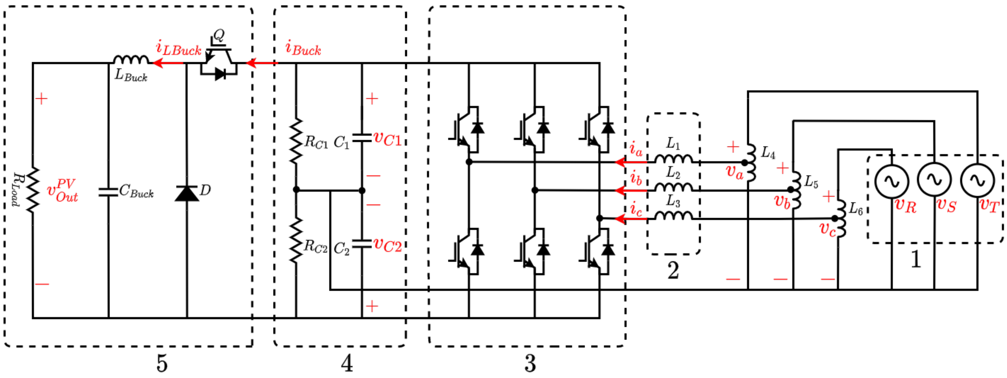
3. Programmable Electronic Load: Implemented Topology

This section presents the implemented topology of the PEL (see Figure 7). This topology has five stages from right to left according to power flow direction: (1) The sources v R , v S , and v T represent the connection with the electrical grid with a neutral line. The auto-transformer composed of L 4 , L 5 , and L 6 allow a reduction of the voltage level and a balancing of the three-phase grid voltages. (2) Inductors L 1 , L 2 , and L 3 are the filters to coupling the grid with a voltage source inverter (VSI). (3) The VSI corresponds to a three-phase, four-wire inverter. (4) The DC bus (split with a neutral line) is responsible for storing energy and allows us to stabilize the DC voltage. Resistances R C 1 and R C 2 are responsible for balancing the voltage in capacitors C 1 and C 2 . (5) The Buck converter dissipates the active power when the PEL absorbs energy from the AC power grid by means of R l o a d . More information concerning Buck converters and their applications in MGs can be consulted in [31].

3.1. VSI Mathematical Model

The mathematical modeling of the VSI is presented in Equation (5), and the procedure to obtain the equations can be consulted in [32]. In this case, v D C = v C 1 v C 2 is the total DC bus voltage with C 1 = C 2 = C and resistances R C 1 = R C 2 = R o . Current i a b c and voltage v a b c are the vectors which represent the current of PEL and the grid voltage for each phase ( a , b , c ) respectively:
L d i a b c d t = v D C 2 u a b c + v a b c C d v D C d t = i a b c u a b c T v D C R o .
The logic of control is given by Equation (6), and the control function (F) is defined as u a b c = 2 F 1 , 3 , 5 1 for the switches of the inverter upper level ( F 1 , 3 , 5 ) whereas u a b c = 1 2 F 2 , 4 , 6 for the switches of the inverter low level ( F 2 , 4 , 6 ):
u a b c = 1 if F 1 , 3 , 5 = o n and F 2 , 4 , 6 = o f f 1 if F 1 , 3 , 5 = o f f and F 2 , 4 , 6 = o n .
The representation of Equation (5) in the d q reference system is given by Equation (7), where v p c c is the voltage in the connection point:
L d i d d t = v D C 2 u d L ω i d + v d p c c L d i q d t = v D C 2 u q + L ω i d + v d p c c C d v D C d t = i d u d + i q u q v D C R o .

3.2. Mathematical Model of the DC/DC Buck Converter

The Buck converter controls the DC bus voltage by means of energy dissipation through R L o a d . Its mathematical model is given by Equation (8) [31] for the input current i B u c k and the converter output voltage v o u t P V , where u B u c k is the variable that represents the control signal of the Buck converter switch:
L B u c k d i B u c k d t = v D C u B u c k v o u t P V C B u c k d v o u t P V d t = i L B u c k v o u t P V R L o a d .

3.3. Transfer Functions

The procedure to obtain the transfer functions consists of applying the d q transformation and state-space representation to the mathematical model [32]. Starting from the large-signal model shown in (7), the PEL small-signal model can be obtained by using the following state-space formulation:
x ˙ = A x + B u y = C x + D u
with
A = f x , u x i x e , u e B = f x , u u i x e , u e C = h x , u x i x e , u e D = h x , u u i x e , u e ,
where x i corresponds to the ith state variable, f ( x , u ) corresponds to each equation of Model (7), and h ( x , u ) are the equations that relate state and output variables. It is considered that h ( x , u ) = x . The subscripts e in (10) are state variables ( x e ) and input variables ( u e ) in their rated values; they are represented by using capital letters.
A, B, C, and D matrices are obtained by using the following definitions: state variables x = i S d , i S q , v D C T ; input variables u = u d , u q , v p c c d , v p c c q T ; and output variables that are equal to state variables as y = x = i S d , i S q , v D C T .
The PEL state model is obtained after applying (9) and (10) over the model (7). This representation linearizes the system around an operation point. The representation of matrices A and B is as follows:
A = R L L ω U d 2 L ω R L L U q 2 L U d C U q C 1 R o C B = V D C 2 L 0 1 L 0 0 V D C L 0 1 L I S d C I S q C 0 0 .
Matrix C corresponds to a 3 × 3 identity matrix whereas matrix D is a 4 × 3 matrix of zeros. The state-space representation is in the time domain. Equation (12) yields the frequency domain representation as follows:
G ( s ) = 1 d e t ( s I A ) C a d j ( s I A ) T B + D .
The transfer functions to design the control system of the PEL are given by Equations (13) and (14). Equation (13) presents the transfer function ( G i d ( s ) ) for the current associated with the active power ( i d ) with respect to its modulation variable ( u d ). Equation (14) presents the transfer function ( G i q ( s ) ) for the current associated with reactive power ( i q ) with respect to its modulation variable ( u q ):
G i d ( s ) u d = 2 C L R o V D C s 2 + ( 2 I d L R o U d 2 L V D C ) s 2 I d L R o U q ω R o ( U q ) 2 V D C 4 C L 2 R o s 3 + ( 4 L 2 ) s 2 + ( 4 C L 2 R o ω 2 + 2 L R o ( U d ) 2 + 2 L R o ( U q ) 2 ) s + 4 ω 2 L 2
G i q ( s ) u q = 2 C L R o V D C s 2 + ( 2 I q L R o U q 2 L V D C ) s + 2 I q L R o U d ω R o ( U d ) 2 V D C 4 C L 2 R o s 3 + ( 4 L 2 ) s 2 + ( 4 C L 2 R o ω 2 + 2 L R o ( U d ) 2 + 2 L R o ( U q ) 2 ) s + 4 ω 2 L 2 .
For the external loop control, it is necessary to deduce a transfer function for the voltage in the DC bus ( G v D C ( s ) ) with respect to its input variable ( i d ) (please see Equation (15)). This Equation was deduced by considering that i d and i q are modeled as sources of controlled current in (7) and applying again the procedure of Equations (9) and (12):
G v D C ( s ) i d = R o U d R o C s + 1 .
The procedure for obtaining the transfer function that permits regulating the output voltage in the Buck converter is obtained after applying the procedure of Equations (9) and (12) over Model (8). In this case, the transfer function is given by Equation (16):
V o u t P V U B u c k = V D C R L o a d R L o a d L B u c k C B u c k s 2 + L B u c k s + R L o a d .

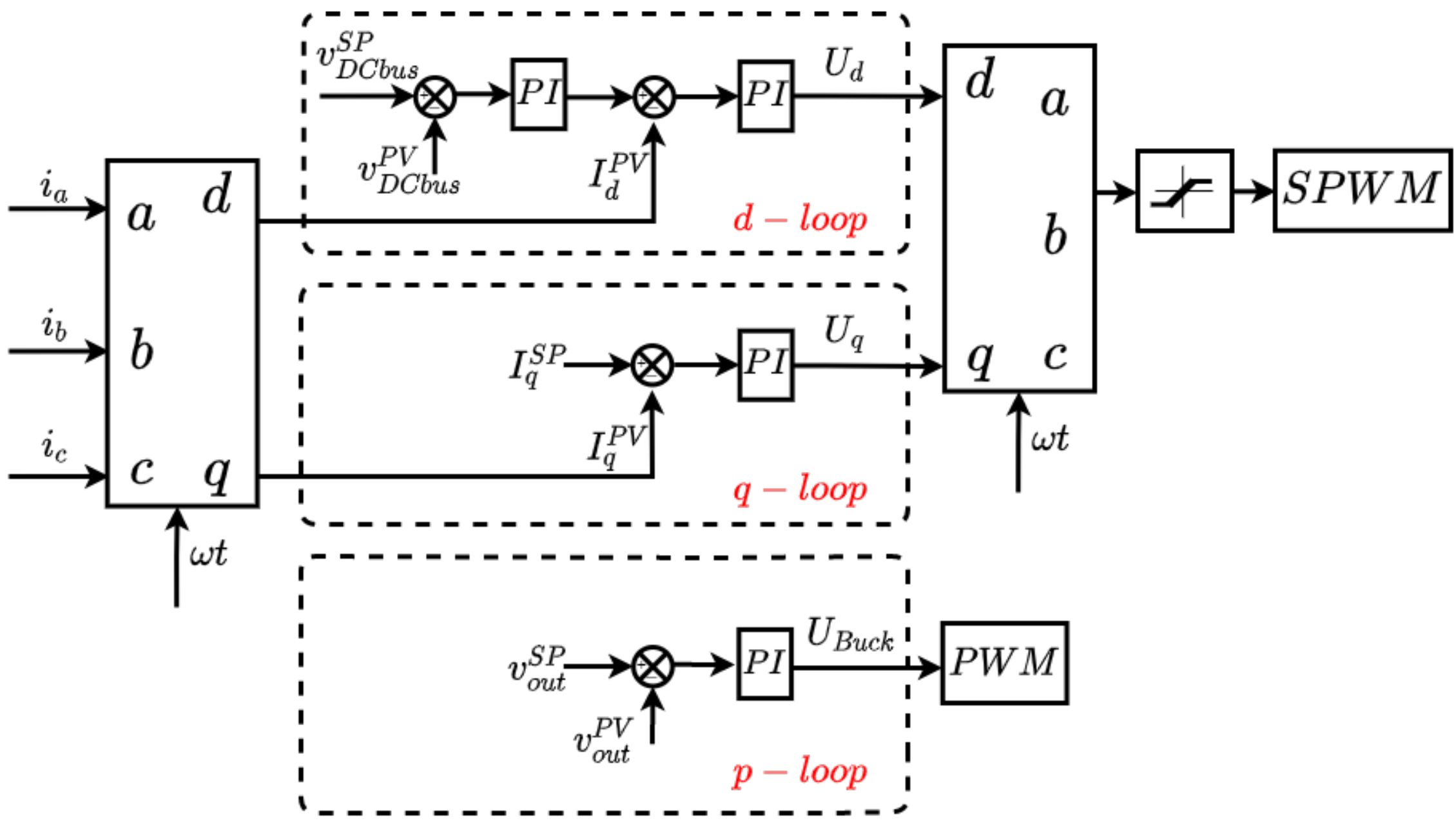
4. Programmable Electronic Load: Control System

This section presents the implemented PEL control system. The control has as its main function the emulation of different load profiles, and at the same time, keeping the DC bus voltage stable. Figure 8 shows the implemented control system that is described as follows.
Currents i a , i b , and i c correspond to the measured PEL line currents, whereas signal ω t is obtained from a phase lock loop (PLL) for synchronizing AC voltages with the control system. i a , i b , i c , and ω t are processed by using an a b c to d q transformation block. The outputs of this block are the current on the d axis ( I d P V ), and the current on q axis ( I q P V ). The measured voltage at the DC bus of the VSI is v D C b u s P V .
The load profiles implemented in this paper are made of active and reactive currents; the VSI and Buck converter are coupled for this purpose. The VSI is controlled by using two controllers (d-loop and q-loop). The reactive power of the PEL is controlled by using the q-loop controller with the setpoint I q S P . The d-loop corresponds to a cascade control responsible for controlling the active power of the PEL. The Buck converter is controlled by using the p-loop controller for dissipating the excess of power in the R l o a d when the PEL is absorbing energy. The control logic of the p-loop and d-loop are not related; nevertheless, both physically interact on the DC bus. The p-loop takes energy from the DC bus and the d-loop gives energy to the DC bus from the electrical grid.
The inputs and outputs of the three control loops are described as follows:
  • The d-loop is a cascade control. Its external loop regulates the voltage in the DC bus whereas its inner loop controls the current of the d-axis. v D C b u s S P is the set point of the DC bus voltage whereas the measured DC voltage is v D C b u s P V . The PI controller of the external loop gives reference to the inner loop, compared with the measured current in the d-axis I d P V . The control signal of this cascade system ( U d ) is one of the two inputs of dq to abc transformation. The parameters for this control are presented in Table 1.
  • The q-loop is a PI control loop where I q S P is the set point, and I q P V is the measured current in the q-axis. The control signal of this system ( U q ) is the other input of the dq to abc transformation block. The output of the dq to abc transformation block passes by a limiter in order to avoid over-modulation in the SPWM block.
  • The p-loop is in charge of determining the dissipated active power in R l o a d , adjusting the output voltage v o u t P V with the Buck converter. The set point is v o u t S P and the measurement is v o u t P V . The control signal of this system ( U B u c k ) is the input of the PWM block. The control parameters for the Buck converter are given in Table 2.

5. Experimental Results

This section presents the experimental results for the implemented PEL. Experimental tests were carried out for several load profiles and for several changes in their operation points. The results show that the PEL behaves adequately, emulating the programmed load profiles and stabilizing the DC bus.

5.1. Experimental Setup

Figure 9 presents the implemented PEL and its main components which are described as follows. (1) The main protection and line contactor that are in charge of protecting and connecting the PEL to the electrical grid. (2) Auxiliary protections that are in charge of protecting each PCB and control circuits. (3) Voltage source of 5 V for polarizing the control system. (4) Voltage source of 15 V for polarizing the trigger drivers of the VSI. (5) PCB for voltage measurement; this PCB measures v a , v b , v c , and v D C b u s P V with differential connection. This PCB is based on AMC1200 integrated circuits. (6) PCB of the digital signal processor (DSP) TMS3202F of Texas Instrument. (7) PCB for current measurement; this PCB measures i a , i b , and i c and is based on ACS714 sensors. (8) Pre-charge bypass contactor. (9) Pre-charge resistors for the DC bus. (10) Control relays which are the interface between the control signals from the DSP and the contactors. (11) Capacitors ( C 1 , C 2 ) and resistors ( R 1 , R 2 ) of the DC bus. (12) Inductors L 1 , L 2 , and L 3 used for grid coupling. (13) IGBT bridge (VSI) coupled with the trigger drivers IRAM136-3063B. The values of parameters of the implemented PEL are summarized in Table 3.

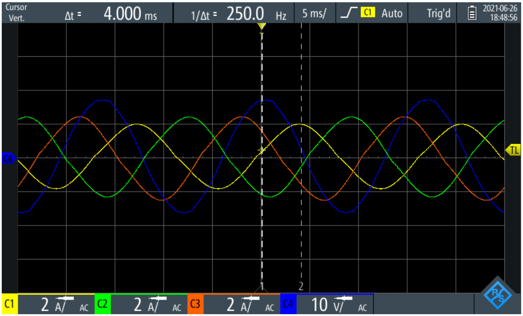
5.2. Emulation of Three-Phase Load Profiles

This section has the purpose of validating the three-phase currents of the PEL when inductive, resistive, and capacitive load profiles are emulated. Figure 10 corresponds to an inductive load profile. This profile was obtained by using i q S P = 4 A as a setpoint, whereas the Buck converter output voltage was set to v o u t S P = 0 V . The oscillogram depicted in Figure 10 plots the voltage and current signals at the AC coupling point versus time. Signal C4 (blue) is the measured voltage in phase a ( v a ) with respect to the neutral point, scaling to 10V per division. Signals C1, C2, and C3 are the line currents i a , i b , and i c (yellow, green, and orange, respectively) with a scale of 2 A per division, whereas the timescale is 5 ms per division. In Figure 10, it can be observed that the measurement cursors located at the maximum values of voltage v a and current i a , both have a time difference of approximately 4 ms; this represents −86.4 ° which emulates an inductive load profile. The difference between measured and theoretical phase angle is due to the PEL active power losses. PEL must have satisfied internal power losses of semiconductors and wires. It can be stated that the implemented controller satisfactorily follows the current reference.
Figure 11 corresponds to a resistive load profile. This profile was obtained by using i q S P = 0 as a setpoint, whereas the Buck converter output voltage was set to v o u t S P = 45 V D C . Taking into account that the R l o a d is 114 Ω and the output voltage v o u t S P is known, the dissipated power in the Buck converter is 17.7 W . It can be seen that v a (blue) and i a (yellow) are in phase.
Figure 12 corresponds to a capacitive load profile. The current setpoint is i q S P = 1.5 A . Because it is not necessary an active power dissipation, the Buck output voltage was set to v o u t S P = 0 . Note that the magnitude of i q S P for the capacitive profile ( 1.5 A ) is lower than the one for the inductive profile ( 4 A ). This is because capacitive profiles require higher DC bus voltages. This phenomenon is consistent with the theory that was previously explained in Section 2.

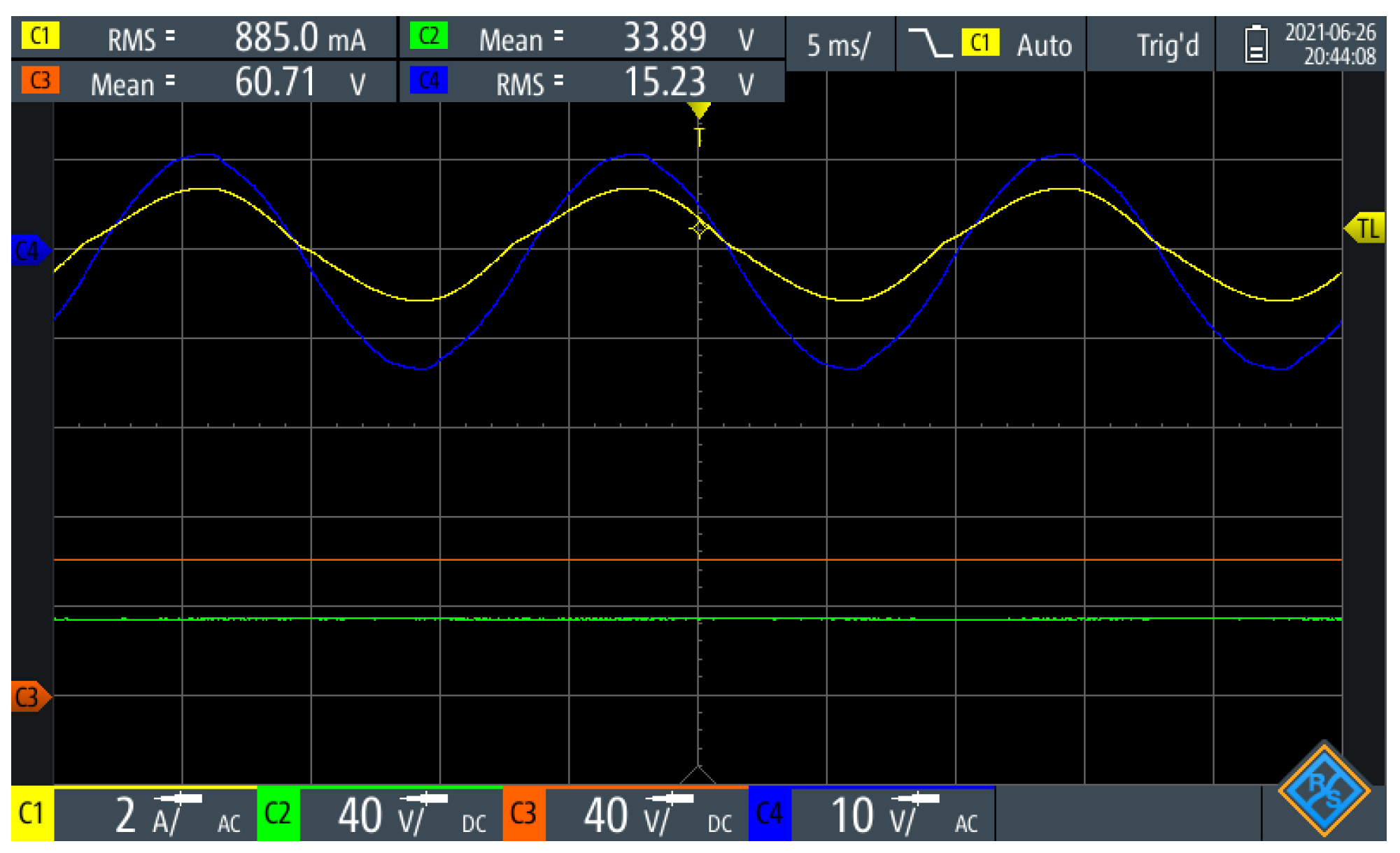
5.3. DC Bus Stability with Different Load Profiles

This section has the purpose of validating the AC and DC voltages of the PEL when inductive, resistive and capacitive load profiles are emulated.
Figure 13 presents the measurements of currents and voltages of the PEL operation when a resistive–capacitive load profile is emulated. Signal C4 (blue) is v a , signal C1 (yellow) is i a , signal C2 (green) is the output voltage of the Buck converter ( v o u t P V ), and signal C3 (orange) is the DC bus voltage ( v D C b u s P V ). The setpoint p-load Buck control loop ( v o u t S P ) was set with a value of 29 V . In this case, the PEL only consumes 7.4 W of active power. The set point I q S P was set to 2 A in the q-load loop.
PEL consumes active and reactive powers with a leading power factor. However, the voltage on the DC bus is not a constant default value and depends on the operating point. Therefore, the cascade controller described in Section 4 is responsible for keeping the DC voltage stable, and at the same time, regulating the direct current consumed from the grid ( i d P V ). The DC output voltage of the Buck converter ( v o u t P V ) allows for the determination of the active power consumed in the load resistor ( R l o a d ). The active power is reflected in the AC network consumption because it is dissipated by the Joule effect in the resistor R l o a d . Generally speaking, the active power dissipated by the Buck converter comes from the energy stored in the DC bus capacitors (C); which, in turn, also comes from the energy supplied by the power grid.
Figure 14 describes an inductive profile. This profile was obtained by using i q S P = 4 A as a setpoint whereas the Buck converter output voltage was set to v o u t S P = 0 V . Figure 15 corresponds to a resistive load profile. This profile was obtained by using i q S P = 4 A as a setpoint whereas the Buck converter output voltage was set to v o u t S P = 0 V . For both cases, the PEL follows the references operating appropriately. The DC bus voltage ( v D C b u s P V ) remains stable under the different PEL operating conditions, evidencing the robustness of the d-loop control loop.

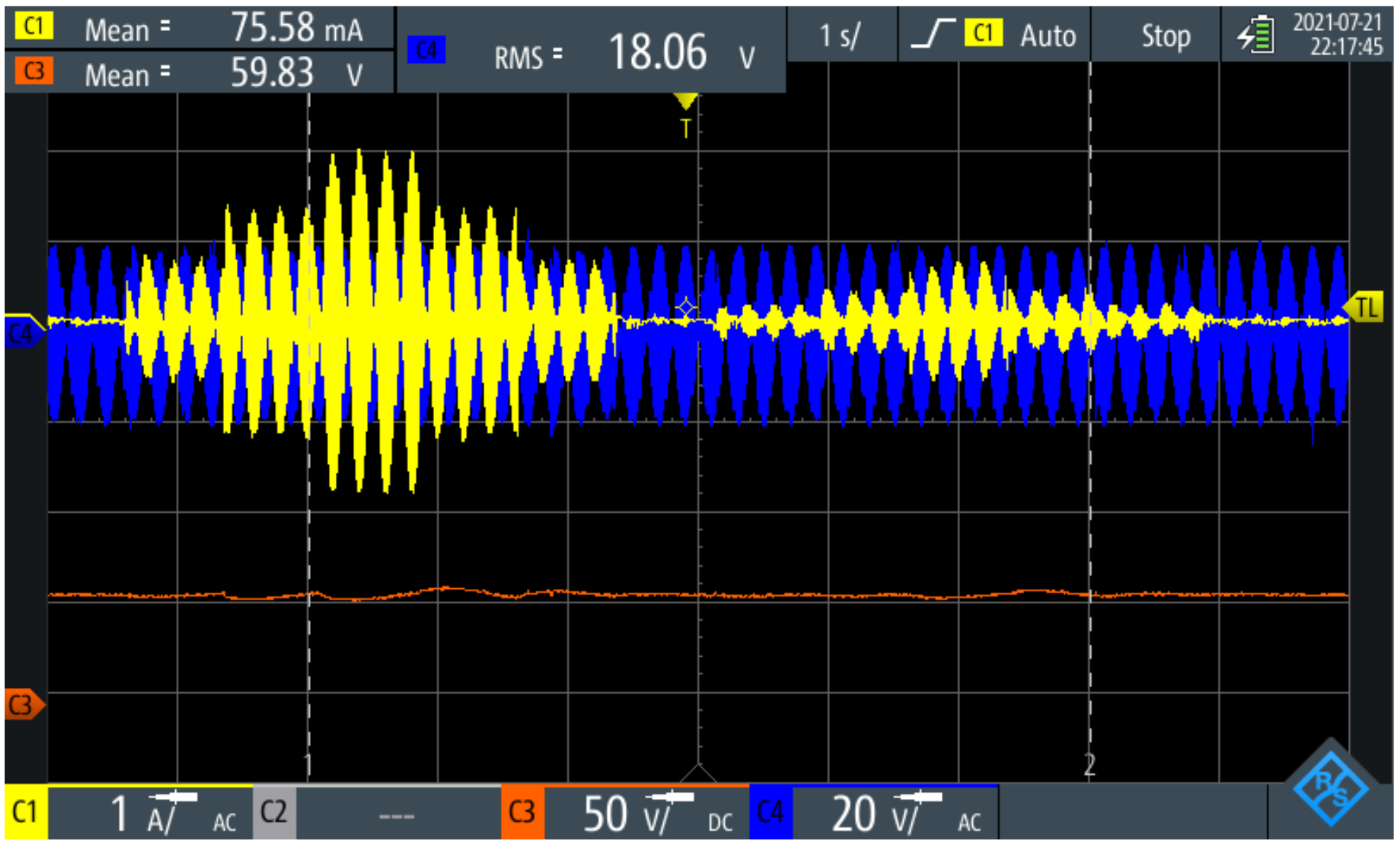
5.4. Transient Behavior of the PEL with Changes in Load Profile

Figure 16 describes the transient behavior of the PEL. Note that the time scale (1 s/divison) is larger than the ones illustrated in previous subsections. The PEL was parameterized to emulate a leading and lagging reactive profile with setpoint steps ( i q S P ) of 0A, −1A, −2A, −2A, −2A, −1A, 0A, 0.25A, 0.5A, 0.5A, 1A, 0.5A, 0.25A, and 0A, changing its magnitude every 750 ms. The sign of the setpoint implies either leading or lagging. One of the conclusions of the principle of operation is that for the same voltage on the DC bus, it is possible to emulate lagging currents of greater magnitude with respect to the magnitudes in leading, which explains the asymmetry of Figure 16. The d-loop cascade control loop is in charge of keeping the DC bus voltage stable; note that C3 signal has over- and under-voltages, accounting for the disturbance and the d-loop control action. In conclusion, the PEL emulates different profiles with variations in time, remaining with stable control.

6. Conclusions

This paper presented the development of an AC three-phase PEL which allows the emulation of load profiles that are useful for testing MGs equipment. The four zones or quadrants obtained determine the PEL operation modes allowing us to establish the conditions that are necessary for programming the load profiles. There were also obtained the power and current limits which establish the control limitations. Three control loops were implemented in the PEL. Two controllers (d-loop and q-loop) were used for the VSI, a d-loop to control the active power and a q-loop to control the reactive power. The control of the Buck converter consists of a p-loop controller which permits the dissipation of excess of active power.
The load profiles shown in the results section allow us to validate the proper operation of the PEL. The emulation of three-phase currents was carried out in pure reactive power and active power scenarios. The DC voltages of the device remained stable, due to the robust parameterization of the control loops. Finally, the transient behavior was evaluated, and the DC bus disturbances were stabilized by the control system.

Author Contributions

Conceptualization, L.F.S.-M., N.M.-G. and J.B.C.-Q.; data curation, L.F.S.-M. and P.A.G.-V.; formal analysis, L.F.S.-M., N.M.-G. and J.B.C.-Q.; funding acquisition, J.B.C.-Q., J.M.L.-L. and N.M.-G.; investigation, L.F.S.-M., N.M.-G. and J.B.C.-Q.; methodology, L.F.S.-M., N.M.-G. and J.B.C.-Q.; project administration, N.M.-G. and J.M.L.-L.; resources, L.F.S.-M., N.M.-G. and J.B.C.-Q.; supervision, N.M.-G., J.M.L.-L. and J.B.C.-Q.; visualization, L.F.S.-M., N.M.-G. and J.B.C.-Q.; writing—original draft, J.R.O.-C., L.F.S.-M. and P.A.G.-V.; writing—review and editing, J.M.L.-L., L.F.S.-M., J.R.O.-C., P.A.G.-V. and N.M.-G. All authors have read and agreed to the published version of the manuscript.

Funding

This research was funded by the Colombia Scientific Program within the framework of the so-called Ecosistema Científico (Contract No. FP44842- 218-2018).

Institutional Review Board Statement

Not applicable.

Informed Consent Statement

Not applicable.

Data Availability Statement

Not applicable.

Acknowledgments

The authors gratefully acknowledge the support from the Colombia Scientific Program within the framework of the call Ecosistema Científico (Contract No. FP44842- 218-2018). The authors also want to acknowledge Universidad de Antioquia for its support through the project “estrategia de sostenibilidad”.

Conflicts of Interest

The authors declare that they have no conflict of interest.

References

  1. Telaretti, E.; Dusonchet, L. Battery storage systems for peak load shaving applications: Part 2: Economic feasibility and sensitivity analysis. In Proceedings of the 2016 IEEE 16th International Conference on Environment and Electrical Engineering (EEEIC), Florence, Italy, 7–10 June 2016; pp. 1–6. [Google Scholar] [CrossRef]
  2. Shen, J.; Jiang, C.; Li, B. Controllable Load Management Approaches in Smart Grids. Energies 2015, 8, 11187–11202. [Google Scholar] [CrossRef] [Green Version]
  3. Geng, Z.; Gu, D.; Hong, T.; Czarkowski, D. Programmable Electronic AC Load Based on a Hybrid Multilevel Voltage Source Inverter. IEEE Trans. Ind. Appl. 2018, 54, 5512–5522. [Google Scholar] [CrossRef]
  4. Pudur, R.; Srivastava, V.K. Performance Study of Electronic Load Controller for Integrated Renewable Sources. In Proceedings of the 2018 2nd International Conference on Electronics, Materials Engineering Nano-Technology (IEMENTech), Kolkata, India, 4–5 May 2018; pp. 1–6. [Google Scholar] [CrossRef]
  5. Serban, I.; Ion, C.; Marinescu, C.; Cirstea, M.N. Electronic Load Controller for Stand-Alone Generating Units with Renewable Energy Sources. In Proceedings of the IECON 2006 32nd Annual Conference on IEEE Industrial Electronics, Paris, France, 6–10 November 2006; pp. 4309–4312. [Google Scholar] [CrossRef]
  6. Kanadhiya, M.C.; Bohra, S.S. Simulation Analysis of Active Programmable Electronic AC Load. In Proceedings of the 2018 3rd International Conference for Convergence in Technology (I2CT), Pune, India, 6–8 April 2018; pp. 1–6. [Google Scholar] [CrossRef]
  7. Rosas-Caro, J.C.; Peng, F.Z.; Cha, H.; Rogers, C. Z-Source-Converter-Based Energy-Recycling Zero-Voltage Electronic Loads. IEEE Trans. Ind. Electron. 2009, 56, 4894–4902. [Google Scholar] [CrossRef]
  8. Shinde, U.K.; Kadwane, S.G.; Gawande, S.P.; Keshri, R. Solar PV emulator for realizing PV characteristics under rapidly varying environmental conditions. In Proceedings of the 2016 IEEE International Conference on Power Electronics, Drives and Energy Systems (PEDES), Trivandrum, India, 14–17 December 2016; pp. 1–5. [Google Scholar] [CrossRef]
  9. Zhou, Z.; Macaulay, J. An Emulated PV Source Based on an Unilluminated Solar Panel and DC Power Supply. Energies 2017, 10, 2075. [Google Scholar] [CrossRef] [Green Version]
  10. Averous, N.R.; Stieneker, M.; De Doncker, R.W. Grid emulator requirements for a multi-megawatt wind turbine test-bench. In Proceedings of the 2015 IEEE 11th International Conference on Power Electronics and Drive Systems, Sydney, Australia, 9–12 June 2015; pp. 419–426. [Google Scholar] [CrossRef]
  11. Biligiri, K.; Harpool, S.; von Jouanne, A.; Amon, E.; Brekken, T. Grid emulator for compliance testing of Wave Energy Converters. In Proceedings of the 2014 IEEE Conference on Technologies for Sustainability (SusTech), Portland, OR, USA, 24–26 July 2014; pp. 30–34. [Google Scholar] [CrossRef]
  12. Lohde, R.; Fuchs, F.W. Laboratory type PWM grid emulator for generating disturbed voltages for testing grid connected devices. In Proceedings of the 2009 13th European Conference on Power Electronics and Applications, Barcelona, Spain, 8–10 September 2009; pp. 1–9. [Google Scholar]
  13. Serna-Montoya, L.F.; Cano-Quintero, J.B.; Muñoz-Galeano, N.; López-Lezama, J.M. Programmable Electronic AC Loads: A Review on Hardware Topologies. In Proceedings of the 2019 IEEE Workshop on Power Electronics and Power Quality Applications (PEPQA), Manizales, Colombia, 30–31 May 2019; pp. 1–6. [Google Scholar] [CrossRef]
  14. Davis, P.N.; Wright, P.S. An Electronic Load to Verify Harmonic Emission Compliance. IEEE Trans. Instrum. Meas. 2017, 66, 1446–1453. [Google Scholar] [CrossRef]
  15. Wang Shaokun, H.Z.; Chuanbiao, P. A repetitive control strategy of AC electronic load with energy recycling. In Proceedings of the International Technology and Innovation Conference 2009 (ITIC 2009), Xi’an, China, 12–14 October 2009; p. 3. [Google Scholar]
  16. Nujithra, T.; Premarathne, U. Investigation of Efficient Heat Dissipation Mechanisms for Programmable DC Electronic Load Design. In Proceedings of the 2018 8th International Conference on Power and Energy Systems (ICPES), Colombo, Sri Lanka, 21–22 December 2018; pp. 201–206. [Google Scholar] [CrossRef]
  17. Peng, J.; Chen, Y.; Fang, Y.; Jia, S. Design of Programmable DC Electronic Load. In Proceedings of the 2016 International Conference on Industrial Informatics—Computing Technology, Intelligent Technology, Industrial Information Integration (ICIICII), Wuhan, China, 3–4 December 2016; pp. 351–355. [Google Scholar] [CrossRef]
  18. Tsang, K.M.; Chan, W.L. Fast Acting Regenerative DC Electronic Load Based on a SEPIC Converter. IEEE Trans. Power Electron. 2012, 27, 269–275. [Google Scholar] [CrossRef]
  19. Kazerani, M. A high-performance controllable AC load. In Proceedings of the 2008 34th Annual Conference of IEEE Industrial Electronics, Vigo, Spain, 4–7 June 2008; pp. 442–447. [Google Scholar] [CrossRef]
  20. Srinivasa Rao, Y.; Chandorkar, M.C. Real-Time Electrical Load Emulator Using Optimal Feedback Control Technique. IEEE Trans. Ind. Electron. 2010, 57, 1217–1225. [Google Scholar] [CrossRef]
  21. Zhang, W.; Zhang, X. A novel AC electronic load based on hysteresis current control scheme. In Proceedings of the 2011 International Conference on Electrical and Control Engineering, Yichang, China, 16–18 September 2011; pp. 1913–1916. [Google Scholar] [CrossRef]
  22. Aurilio, G.; Gallo, D.; Landi, C.; Luiso, M. AC electronic load for on-site calibration of energy meters. In Proceedings of the 2013 IEEE International Instrumentation and Measurement Technology Conference (I2MTC), Minneapolis, MN, USA, 6–9 May 2013; pp. 768–773. [Google Scholar] [CrossRef]
  23. Friedli, T.; Kolar, J.W.; Rodriguez, J.; Wheeler, P.W. Comparative Evaluation of Three-Phase AC–AC Matrix Converter and Voltage DC-Link Back-to-Back Converter Systems. IEEE Trans. Ind. Electron. 2012, 59, 4487–4510. [Google Scholar] [CrossRef]
  24. Li, F.; Zou, Y.P.; Wang, C.Z.; Chen, W.; Zhang, Y.C.; Zhang, J. Research on AC electronic load based on back to back single-phase PWM rectifiers. In Proceedings of the 2008 Twenty-Third Annual IEEE Applied Power Electronics Conference and Exposition, Austin, TX, USA, 24–28 February 2008; pp. 630–634. [Google Scholar] [CrossRef]
  25. Zheyu, Z.; Yunping, Z.; Zhenxing, W.; Jian, T. Design and research of three-phase power electronic load. In Proceedings of the 2009 IEEE 6th International Power Electronics and Motion Control Conference, Wuhan, China, 17–20 May 2009; pp. 1798–1802. [Google Scholar] [CrossRef]
  26. Jeong, I.W.; Slepchenkov, M.; Smedley, K.; Maddaleno, F. Regenerative AC Electronic Load with One-Cycle Control. In Proceedings of the 2010 Twenty-Fifth Annual IEEE Applied Power Electronics Conference and Exposition (APEC), Palm Springs, CA, USA, 21–25 February 2010; pp. 1166–1171. [Google Scholar] [CrossRef]
  27. Li, F.; Zou, X.; Wang, C.Z.; Chen, W. Research on AC electronic load for testing ac power based on dual single-phase PWM converter. High Volt. Eng. 2008, 34, 930–934. [Google Scholar]
  28. Valdez, J.E.; Mayo, J.C.; Rosas, J.C.; Alejo, A.; Llamas, A. Energy Recycling Three-Phase Experimental Setup for Power Flow Control Devices. IEEE Lat. Am. Trans. 2018, 16, 1337–1342. [Google Scholar] [CrossRef]
  29. Kehler, L.B.; Corrêa, L.C.; Ribeiro, C.G.; Trapp, J.G.; Lenz, J.M.; Farret, F.A. Electronically adjustable load for testing three phase ac systems. In Proceedings of the 2013 Brazilian Power Electronics Conference, Gramado, Brazil, 27–31 October 2013; pp. 1082–1087. [Google Scholar]
  30. Novak, D.; Beraki, M.; Villa, G.; García, P. Low-cost programmable three phase load for microgrids labs. In Proceedings of the 2015 IEEE 15th International Conference on Environment and Electrical Engineering (EEEIC), Rome, Italy, 10–13 June 2015; pp. 599–604. [Google Scholar]
  31. Serna-Montoya, L.F.; Buitrago-Lopez, L.A.; Cano-Quintero, J.B.; Muñoz-Galeano, N.; López-Lezama, J.M. Modeling and Simulation of Buck Converters and their Applications in DC Microgrids. Iaeng Int. J. Comput. Sci. 2021, 48, 804–814. [Google Scholar]
  32. Urrea-Quintero, J.H.; Muñoz-Galeano, N.; López-Lezama, J.M. Robust Control of Shunt Active Power Filters: A Dynamical Model-Based Approach with Verified Controllability. Energies 2020, 13, 6253. [Google Scholar] [CrossRef]
Figure 1. PEL operation principle.
Computers 11 00106 g001
Figure 2. Phasor diagram of the PEL current and voltages path.
Computers 11 00106 g002
Figure 4. Operation modes of the PEL: | V P E L | = | V G | with 0 o θ P E L < 360 ° . (a) pure resistive load, (b) resistive-capacitive load, (c) capacitive load, (d) leading source, (e) pure active source, (f) lagging source, (g) pure lagging source, (h) resistive-inductive load, (i) pure resistive load.
Computers 11 00106 g004
Figure 6. Operation modes of the PEL: A 3D representation. (a) magnitude of S, (b) active power, (c) magnitude of I, (d) reactive power.
Computers 11 00106 g006
Figure 7. PEL hardware topology.
Computers 11 00106 g007
Figure 8. PEL control system.
Computers 11 00106 g008
Figure 9. PEL hardware implementation.
Computers 11 00106 g009
Figure 10. Three-phase inductive load profile.
Computers 11 00106 g010
Figure 11. Three-phase resistive load profile.
Computers 11 00106 g011
Figure 12. Three-phase capacitive load profile.
Computers 11 00106 g012
Figure 13. Resistive-capacitive load profile and DC voltages.
Computers 11 00106 g013
Figure 14. Inductive load profile and DC voltages.
Computers 11 00106 g014
Figure 15. Resistive load profile and DC voltages.
Computers 11 00106 g015
Figure 16. v D C b u s P V and variable reactive loads profiles.
Computers 11 00106 g016
Table 1. PEL control parameters.
ParametersValue
External d-loop   K c v d c 0.026
T i v d c 0.015
Inner d-loop   K c i d 0.1
T i i d 0.0008
q-loop   K c i q 0.108069
T i i q 0.0008
Table 2. Buck control parameters.
ParametersValue
K c B u c k 0.074532
T i B u c k 0.32
Table 3. Implemented PEL parameters.
ParametersSymbolValue
Inductances L 1 23.7 mH
L 2 23.7 mH
L 3 23.7 mH
L B u c k 23.7 mH
Capacitances C 1 , C 2 4400 uF
C B u c k 2700 uF
Resistances R 1 , R 2 30 k Ω
R l o a d 114 Ω
V i n PEL v a 208 V
PEL apparent power S P E L 1.8 kVA
DC bus voltage v D C b u s S P 60 V
Oscilloscope R & S ® R T H 1004
Publisher’s Note: MDPI stays neutral with regard to jurisdictional claims in published maps and institutional affiliations.

