1. Introduction
In the passing years, as the number of electric vehicles, charging piles, and intelligent electronic equipment is on the rise, there is a sustained and strong demand for power MOSFET. Despite those wide bandgap semiconductor power devices such as SiC and GaN developing in leaps and bounds, silicon devices still occupy the largest market share due to their low cost and mature technology. A silicon-on-insulator (SOI) laterally diffused metal-oxide-semiconductor (LDMOS) devices offer the advantages of high speed, low loss, and easy integration and are widely used in power integrated circuits [
1,
2,
3,
4,
5]. Breakdown voltage (
BV) is an important performance indicator of the SOI LDMOS and comprises the static
BV (
StBV) and the transient
BV (
TrBV). An electron inversion layer is formed under the buried oxide (BOX) of the SOI LDMOS in static conditions, such that there is no deep depletion (DD) effect in the substrate, which sustains very little
StBV [
6,
7]. Thus, the device has low
StBV. Scholars have obtained many results after long-term research on
StBV. Some of these results have been obtained using an analytical model of
StBV [
8,
9,
10,
11,
12,
13,
14], and others are related to new structures [
15,
16,
17,
18,
19,
20,
21,
22,
23,
24,
25,
26,
27], in some of which
StBV can reach more than 1000 V [
25,
26,
27]. However, when a device is turned off rapidly, there is insufficient time for an electron inversion layer to form under the BOX, which can induce a DD effect in the substrate. The depletion layer in the substrate can sustain a portion of
TrBV [
6]. E. Napoli proposed a one-dimensional
TrBV analytical model [
7] and performed simulations and experiments [
6,
28,
29] that verified that an appropriate reduction in the substrate doping concentration (
Psub) of the SOI LDMOS can increase
TrBV. In [
30], a new device structure is proposed that achieves a good trade-off between
TrBV and specific on-resistance (
Ron,sp). Like
StBV,
TrBV is determined by the smaller of the lateral breakdown voltage (
BVlat) and the vertical breakdown voltage (
BVver). Studies have shown that although reducing the
Psub can promote expansion of the depletion layer and increase
BVver, the surface field (RESURF) effect is reduced [
31]. An extremely low
Psub can lead to an increase in the surface electric field at the source and premature breakdown, thus reducing
BVlat and resulting in a substantial decrease in
TrBV [
31]. Therefore, the doping concentration in the drift region (
Nd) needs to be reduced simultaneously to obtain high
TrBV [
31], whereby
Ron,sp is also considerably increased. Double RESURF, step doping in the drift region, and linear variable doping in the drift region techniques are commonly applied to improve
BVlat of SOI LDMOS devices [
32,
33,
34,
35]. If
BVlat limits
TrBV, these three techniques can also enhance
TrBV. SOI LDMOS with a P-top layer is called a double RESURF SOI LDMOS (D-RESURF SOI LDMOS), whose P-top layer can improve
BVlat and lower
Ron,sp [
33,
34]. The lateral electric field distribution in the drift region of devices with step doping and a linear variable doping profile is more uniform than that of conventional devices. Therefore, they can achieve higher
TrBV at the same drift region length. However, they have high
Ron,sp due to the too-low doping concentration in the drift region near the source optimizing for
TrBV, and these two techniques are often suitable for ultra-thin SOI devices.
TrBV is an important performance indicator for high-speed SOI LDMOS switching devices. To improve TrBV and suppress the increase in Ron,sp, a SPBL was introduced below the BOX of the SOI LDMOS. The SPBL could optimize the lateral and vertical electric fields of the device and improve the TrBV of the device without increasing the Ron,sp. The simulation results showed that the TrBV of SPBL SOI LDMOS was higher than that of SOI LDMOS and D-RESURF SOI LDMOS, and the Ron,sp was lower. As the vertical electric field was optimized, the turn-off non-breakdown time (Tnonbv) of the SPBL SOI LDMOS was longer than that of the SOI LDMOS and D-RESURF SOI LDMOS.
2. Device Structure and Simulation Settings
Figure 1a shows the SPBL SOI LDMOS device structure and simulation circuit, which differ from those of the conventional SOI LDMOS device shown in
Figure 1c in that there was an SPBL below the BOX. The SPBL was divided into five-step P-type doping regions, and the doping concentration decreased from
P1 to
P5 by the same difference. x and y represent lateral distance from the left edge of the device and vertical distance from the top silicon surface, respectively. When the device is turned off, the high-concentration doping region of the SPBL near the source can enhance the RESURF effect and reduce the surface electric field at the source, whereas the low-concentration doping region near the drain promotes the downward expansion of the substrate depletion layer. After the SPBL is depleted, the negative charges in the SPBL exhibit a stepped distribution. This charge distribution has a significant modulation effect on the lateral electric field in the drift region, which causes the surface electric field in the middle to rise. The enhancement of the RESURF effect by the SPBL can decrease
Psub. Therefore, the SPBL enables the device to maintain a small
Ron,sp and increases
BVlat and
BVver.
Figure 1b shows the D-RESURF SOI LDMOS. A P-type doping layer, namely the P-top layer, is on the top of the drift region.
Ptop and
ttop are the doping concentration and depth of the P-top layer, respectively. At high
Nd, the source surface electric field of SOI LDMOS increases rapidly with the increase of drain voltage. However, the P-top layer in D-RESURF SOI LDMOS can effectively reduce the increasing speed of the surface electric field at the source and obtain higher
StBV. If optimized for
StBV, the
Nd of the D-RESURF SOI LDMOS is twice that of SOI LDMOS. In other words, the
Ron,sp of the D-RESURF SOI LDMOS is smaller than that of SOI LDMOS at the same
StBV. For
TrBV, the P-top layer can also enhance the RESURF effect, maintain high
BV, and obtain lower
Ron,sp. As mentioned in the introduction, most step doping SOI LDMOS and linear variable doping SOI LDMOS are usually ultra-thin SOI devices, and their
Ron,sp is high. Therefore, they were not added to the paper as a reference.
Step doping profile can be achieved by adjusting the implantation window width and multiple ion implantations [
34]. The main manufacturing process of the SPBL SOI LDMOS is shown in
Figure 2. First, a P-type substrate was lithographically aligned, followed by boron-ion implantation from the window to form the first doping region. Next, the window width was doubled to the right, and another boron-ion implantation was performed to form the second doped region. After five consecutive ion implantations, a SPBL was formed, as in
Figure 2c. Then, SiO
2 was deposited on the P-type substrate to form a BOX; the BOX and substrate were treated with double-sided lithography for alignment marks, and the SiO
2 was planarized. Finally, the n-type SOI layer was bonded to the BOX, the SOI layer was thinned, and the lithography was aligned with the marks. The rest of the SPBL SOI LDMOS manufacturing steps are compatible with the standard manufacturing process of the SOI LDMOS. Device fabrication steps and costs increase with the number of doping regions. Therefore, the number was two or three, and the cost could be effectively controlled.
The device parameters of the SOI LDMOS and the D-RESURF SOI LDMOS are listed in
Table 1, while those of the D-RESURF SOI LDMOS are described later. To make a fair comparison of the
TrBVs of the three devices, their
Psub was set to 2 × 10
14 cm
−3, and the
Nd of the SOI LDMOS was optimized to 2.4 × 10
15 cm
−3 based on the
TrBV. To obtain a small
Ron,sp in the SPBL SOI LDMOS and the D-RESURF SOI LDMOS,
Nd was set to 5 × 10
15 cm
−3. Optimized for
TrBV and
Ron,sp,
Ptop and
ttop in the D-RESURF SOI LDMOS were 1.1 × 10
16 cm
−3 and 1 μm, respectively. The other parameters of this device were the same as in SOI LDMOS.
Figure 1 shows the circuit used to simulate the
TrBV of the device [
31]. The source and substrate electrodes of the test device were grounded, gate voltage
Vg was applied to the gate through the gate resistor
Rg, and a fixed drain voltage
Vd was applied to the drain through the drain resistor
Rd.
Rg was set to a small value to ensure that the test device could be quickly turned off. The function of
Rd was to limit the drain current to prevent damage to the device from an excessive current. MEDICI 0.13.2 software of Synopsys was used to perform a two-dimensional simulation of
TrBV in the device. Several models, such as recombination, impact ionization, band-gap narrowing, mobility, and lifetime, were used in the simulation [
30] The temperature (
T) of the simulated device was 300 K by default. The breakdown condition of the device was that the drain current
Id exceeded 1 × 10
−7 A/μm in the off-state. To simulate
TrBV,
Vd was a low positive voltage at which the test device did not break down, and
Vg was decreased from 15 V to 0 V within 0.1 μs to turn the test device off. As a device is quickly turned off, there is insufficient time for an electron inversion layer to form under the BOX, the DD effect is induced in the substrate, which sustains a portion of
Vd [
6,
7,
28,
29]. Then,
Vd is increased until the test device breaks down. The
Vd at breakdown is the
TrBV of the test device. Every time
Vd was changed, a simulation was carried out. This work was done by executing a batch file. If
Vd was greater than or equal to
StBV, the device could be broken down after being in the off-state for a period of time. The time between turning the device off and breakdown is
Tnonbv. To simulate the
Tnonbv,
Vd was a voltage greater than
StBV, and
Vg was decreased from 15 V to 0 V within 0.1 μs to turn the test device off. After a period of time,
Id increased rapidly and exceeded 1 × 10
−7 A/μm in the off-state. Data of
Id with time was stored in a log file by MEDICI.
Tnonbv could be obtained by subtracting the turn-off time from the breakdown time.
3. Results and Discussion
Figure 3 shows the distribution of the charge under the BOX and lateral electric field and the potential of the three devices. The doping concentration of SPBL was reduced from
P1 = 1.5 × 10
16 cm
−3 to
P5 = 1 × 10
15 cm
−3 in five steps of 3.5 × 10
15 cm
−3 each.
TrBV of the SPBL SOI LDMOS was 768 V, which corresponded to a 14.46% increase from that of the SOI LDMOS (671 V) and a 10% increase from that of the D-RESURF SOI LDMOS (698 V). Note that using an
Nd of 5 × 10
15 cm
−3 for the SOI LDMOS and optimizing
Psub to 1.7 × 10
15 cm
−3 with respect to
TrBV resulted in a
TrBV of only 337 V.
Figure 3a shows that compared to those of the SOI LDMOS and the D-RESURF SOI LDMOS, the distribution of equipotential lines in the drift region was more uniform and the substrate depletion layer was deeper in the SPBL SOI LDMOS, that is, the lateral electric field in the drift region was more uniform and both
BVlat and
BVver were larger. The surface potential of SPBL SOI LDMOS in the drift region decreased from 768 V to 0 V with a relatively constant value, and the potential distribution line was relatively straight, as in
Figure 3a. The decrease rate of the surface potential of the other two devices varied greatly, and the two potential distribution lines fluctuated obviously.
Figure 3b shows the distribution of the charge concentration under the BOX for the three devices. There were five steps in the charge distribution below the BOX of the SPBL SOI LDMOS. The charge concentration iwas 1.5 × 10
16 cm
−3 in the first region near the source and decreased to 1 × 10
15 cm
−3 in the fifth region near the drain in fixed step sizes. These four sudden changes in the charge concentration in the SPBL could introduce spikes into the lateral electric field. The charge concentration of 2 × 10
14 cm
−3 under the conventional SOI LDMOS and the D-RESURF SOI LDMOS was evenly distributed, and it did not contribute to the improvement of the electric field in the middle of the drift region.
Figure 3c shows the lateral electric field distribution of the three devices. Unlike with the SOI LDMOS, there were four clear electric field spikes in the lateral electric field inside the BOX (
y = 4.49 μm) and the bottom of the drift region (
y = 3.99 μm) of the SPBL SOI LDMOS, where the lateral electric field in the middle was higher. The surface electric field (
y = 0.001 μm) of the new device was far from the SPBL and was weakly modulated. Although there was no electric field spike on the surface of the drift region of the SPBL SOI LDMOS, the electric field in the middle was uniform and higher than that of the conventional SOI LDMOS and the D-RESURF SOI LDMOS, indicating that the depleted SPBL modulated the lateral electric field in the drift region, which increased the
BVlat of the new device. The P-top layer of the D-RESURF SOI LDMOS could also modulate the surface electric field, but the surface electric field of the D-RESURF SOI LDMOS was not as uniform as that of the SPBL SOI LDMOS.
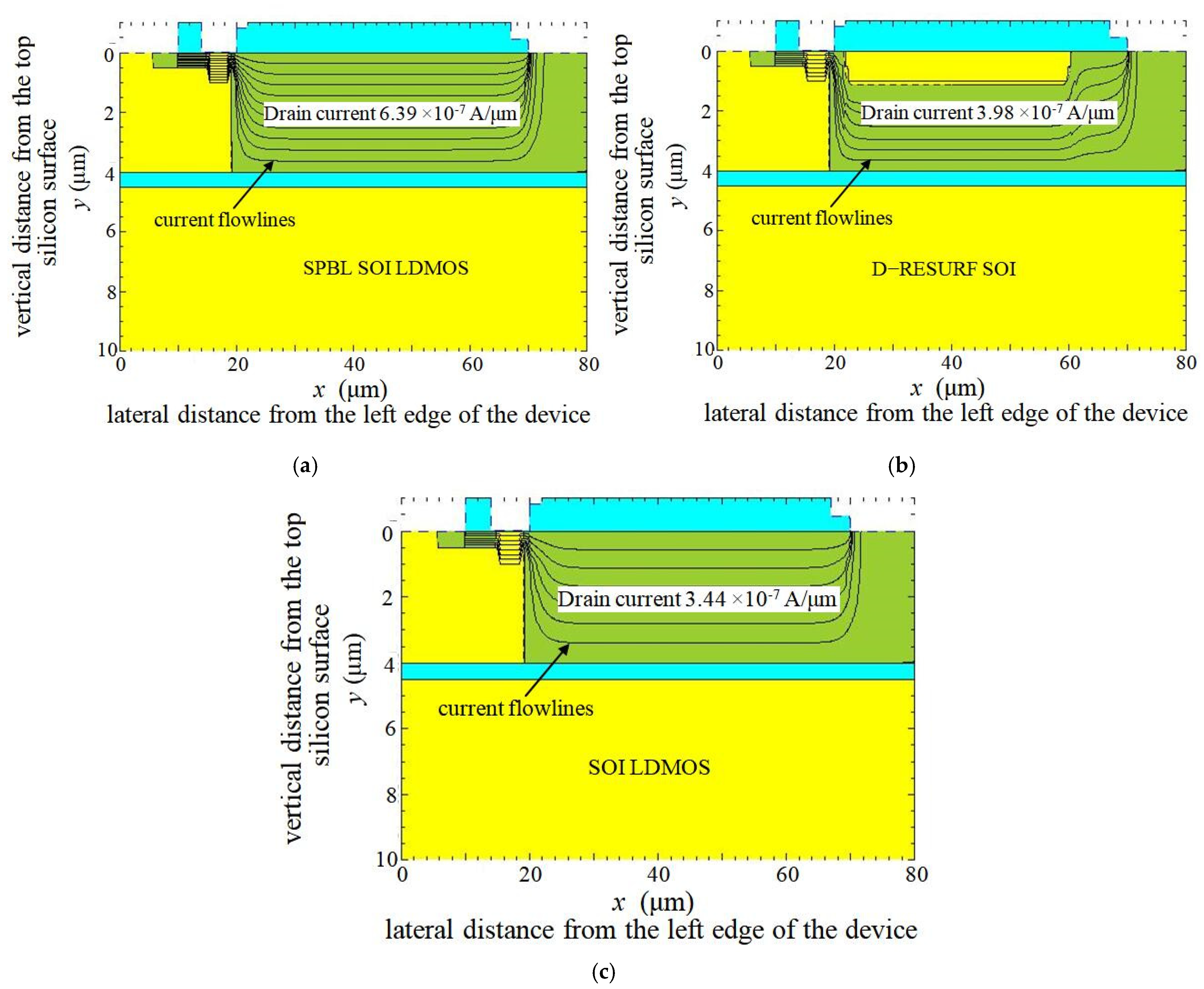
Figure 4 shows the current distribution in the drift region of the three devices at
Vg = 15 V and
Vd = 0.1 V. The
Nd and the current distribution area determine the drain current in the drift region. The
Nd of the SPBL SOI LDMOS was 5 × 10
15 cm
−3, and the current distributed throughout the drift region, as in
Figure 4a. Therefore, its
Id was the largest among those of the three devices. The
Nd of the D-RESURF SOI LDMOS was the same as that of the SPBL SOI LDMOS, and there was no current in the P-top layer, as seen in
Figure 4b. Its
Id was the second largest among those of the three devices. Although the current of the SOI LDMOS distributed throughout the drift region, the
Nd was less than half that of the other two devices. Its current was the smallest among those of the three devices. According to the
Id of these three devices, their
Ron,sp could be calculated. The
Ron,sp was 7.82 Ω·mm
2 for the SPBL SOI LDMOS, which was 46.25% lower than that of the SOI LDMOS (14.55 Ω·mm
2) and 37.74% lower than that of the D-RESURF SOI LDMOS (12.56 Ω·mm
2).
Figure 5 shows the effect of the SPBL doping concentration on
TrBV. The
TrBV of the SOI LDMOS device depended on the smaller of
BVlat and
BVver, both of which were affected by the SPBL doping concentration. Increasing the SPBL doping concentration weakened the surface electric field at the source, which was conducive to increasing
BVlat and hindered the downward expansion of the substrate depletion layer to reduce
BVver. To obtain the maximum
TrBV,
P1 and
P5 needed to be optimized. At a fixed
P5 and a low
P1, the SPBL did not sufficiently weaken the surface electric field at the source, resulting in premature breakdown of the device at the source surface, and
BVlat was lower than
BVver. The
TrBV was limited by
BVlat. Therefore, increasing
P1 could reduce the surface electric field at the source and increase
BVlat, thereby increasing the
TrBV of the device. At a
P5 of 1 × 10
15 cm
−3,
TrBV initially increased with
P1 to a maximum value of 768 V at
P1 = 1.5 × 10
16 cm
−3.
BVlat was equal to
BVver. As
P1 increased, the doping concentration of the other regions (except for the fifth region) also increased accordingly, which enhanced the blocking effect of the SPBL on the downward expansion of the substrate depletion layer, resulting in
BVver being lower than
BVlat. The
TrBV was limited by
BVver. Therefore, as
P1 increased from 1.5 × 10
16 cm
−3 to 1.8 × 10
16 cm
−3,
TrBV was affected by the decrease in
BVver and continued to decrease. In short, when
P5 was constant,
P1 increased from low to high,
BVlat increased from low to high, and
BVver decreased from high to low. When
BVlat was lower than
BVver,
TrBV was determined by
BVlat, and
TrBV increased with
P1. When
BVlat equaled
BVver,
TrBV reached the maximum. When
BVver was less than
BVlat,
TrBV was determined by
BVver, and
TrBV decreased with the increase of
P1. Similarly, increasing
P5 promoted the weakening of the surface electric field at the source and increased
BVlat but hindered the downward expansion of the depletion layer and reduced
BVver. It can be seen from
Figure 5 that for different
P5 values, the trend of
TrBV with increasing
P1 was consistent. The larger
P5, the earlier
TrBV reached a maximum in
P1. However, the increase in
P5 reduced
BVver and thereby the maximum
TrBV.
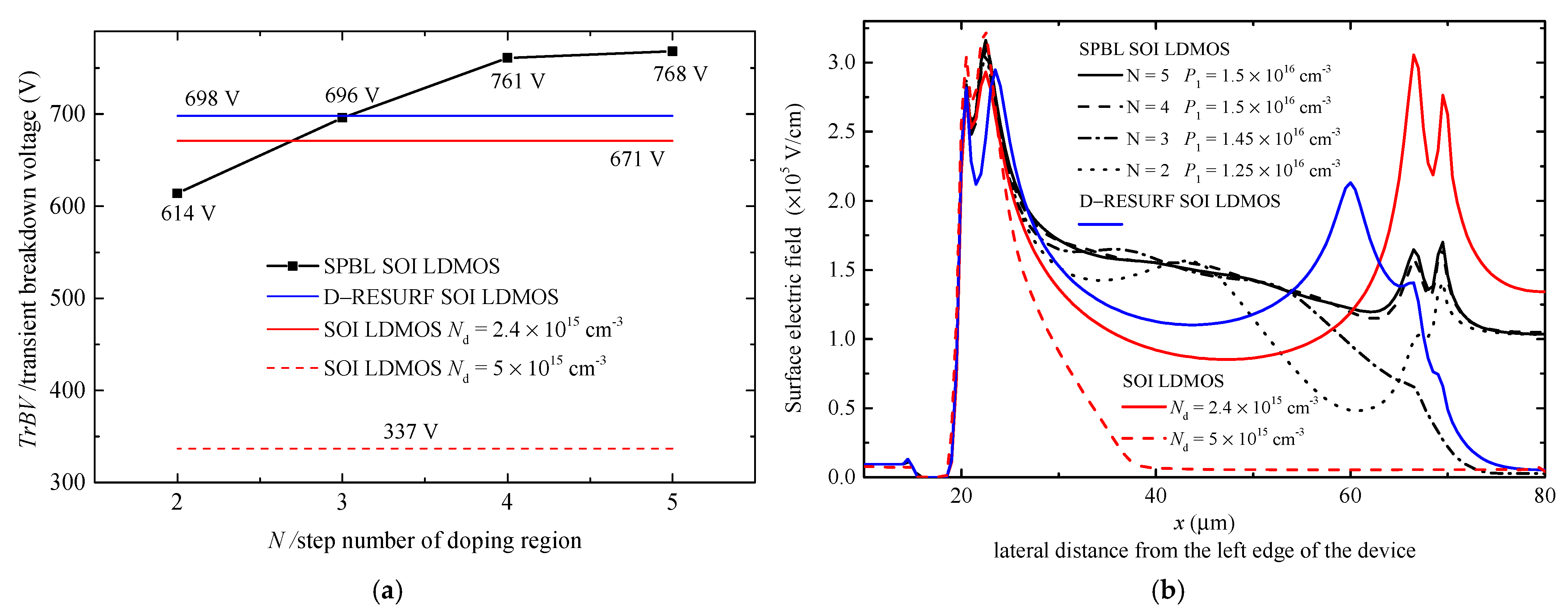
Figure 6 shows the influence of the number of doping regions (
N) of SPBL on
TrBV and surface electric field. The
TrBV of the SPBL SOI LDMOS listed in
Figure 6a was the maximum value that could be gained by optimizing the doping concentration of SPBL at different
N. The
TrBV of the device increased with the
N and then tended to be saturated. In
Figure 6b, the surface electric fields of the SPBL SOI LDMOS were compared at different
N. When
N = 2, there was a comparatively high peak in the middle of the surface electric field, but the electric field near the drain was too low.
TrBV was 614 V. When
N = 3, there were two peaks in the middle of the surface electric field, which made the surface electric field more uniform and the electric field near the drain higher.
TrBV increased to 696 V. When
N = 4, the surface electric field in the middle of the drift region and near the drain was more uniform, and
TrBV was further increased to 761 V. When
N = 5, the surface electric field distribution was almost the same as that of
N = 4, and
TrBV was 768 V and only increases by 7 V. Therefore, with an increase of
N, the SPBL modulated the surface electric field more uniformly, and a higher
TrBV could be obtained. For the SOI LDMOS, the surface electric field at the source was too high at
Nd = 5 × 10
15 cm
−3. The device was prematurely broken down, and its
TrBV was 337 V. When
Nd = 2.4 × 10
15 cm
−3, the surface electric field peaks were at the source and drain, and the electric field at the middle of the drift region was low.
TrBV was increased to 671 V. Compared to that of the SOI LDMOS, the surface electric field of the D-RESURF SOI LDMOS in the drift region was more uniform and higher, and its
TrBV was also 27 V higher. The
Ron,sp of the SPBL SOI LDMOS was the lowest among those of the three devices. At
N = 3, the
TrBV of the SPBL SOI LDMOS was as high as that of the D-RESURF SOI LDMOS and higher than that of the SOI LDMOS. At
N > 3, the
TrBV of the SPBL SOI LDMOS was higher than that of the other two devices.
Turning the device off generates electron-positron pairs in the substrate depletion layer. Under an electric field, the electrons move into and continuously accumulate at the bottom of the BOX, and the holes move to the edge of the depletion layer and recombine with the electrons, thereby continuously thinning the depletion layer [
30]. Therefore, with increasing time, the voltage sustained by the device substrate continuously decreases, and the voltage sustained by the drift region and the BOX continuously increases. The maximum voltage that the drift region and BOX can sustain is approximately equal to
StBV. If
Vd is greater than or equal to
StBV, the device can be broken down after being in the off-state for a period of time.
Tnonbv serves as a reference for the lowest operating frequency of the device [
31].
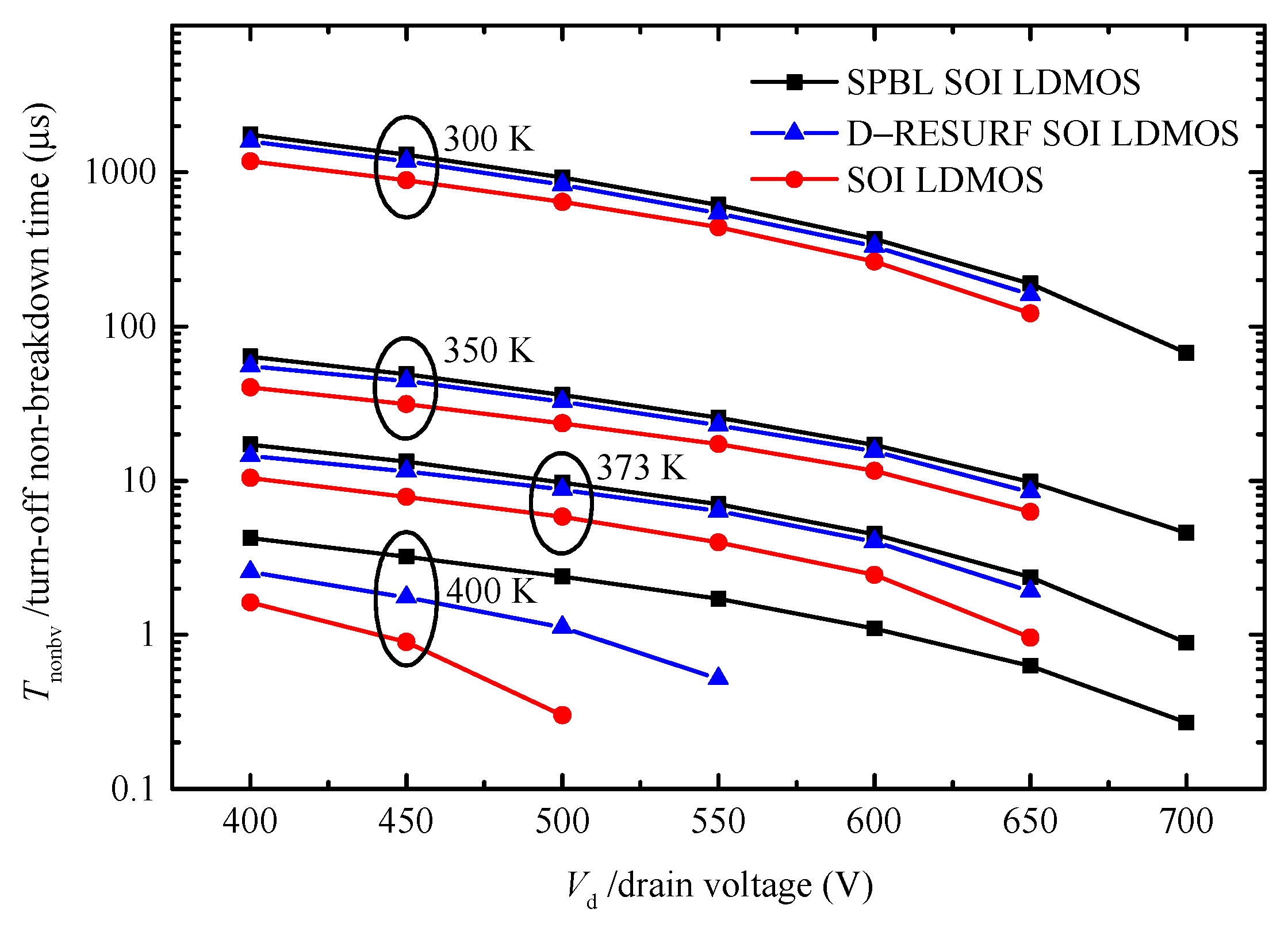
Figure 7 shows the effect of different
Ts and
Vds on
Tnonbv. The higher the
Vd, the more rapid the rate of increase in the voltage sustained by the drift region and BOX, and the smaller the
Tnonbv. The effect of
T on
Tnonbv was more significant. The generation rate of electrons and holes in the substrate depletion layer increased rapidly with
T, resulting in a rapid thinning of the depletion layer and a significant decrease in
Tnonbv.
Figure 7 shows that for a constant
T, the
Tnonbv of the three devices decreased rapidly with increasing
Vd. The
Tnonbv of the three devices decreased sharply with increasing
T. However, for fixed
T and
Vd, the SPBL SOI LDMOS always had a larger
Tnonbv than the SOI LDMOS and the D-RESURF SOI LDMOS did. For a
T of 400 K and
Vd above 500 V, the substrate depletion layer of the SOI LDMOS thinned sufficiently rapidly that the device could no longer be turned off. The D-RESURF SOI LDMOS also could not be turned off when
Vd was higher than 550 V.
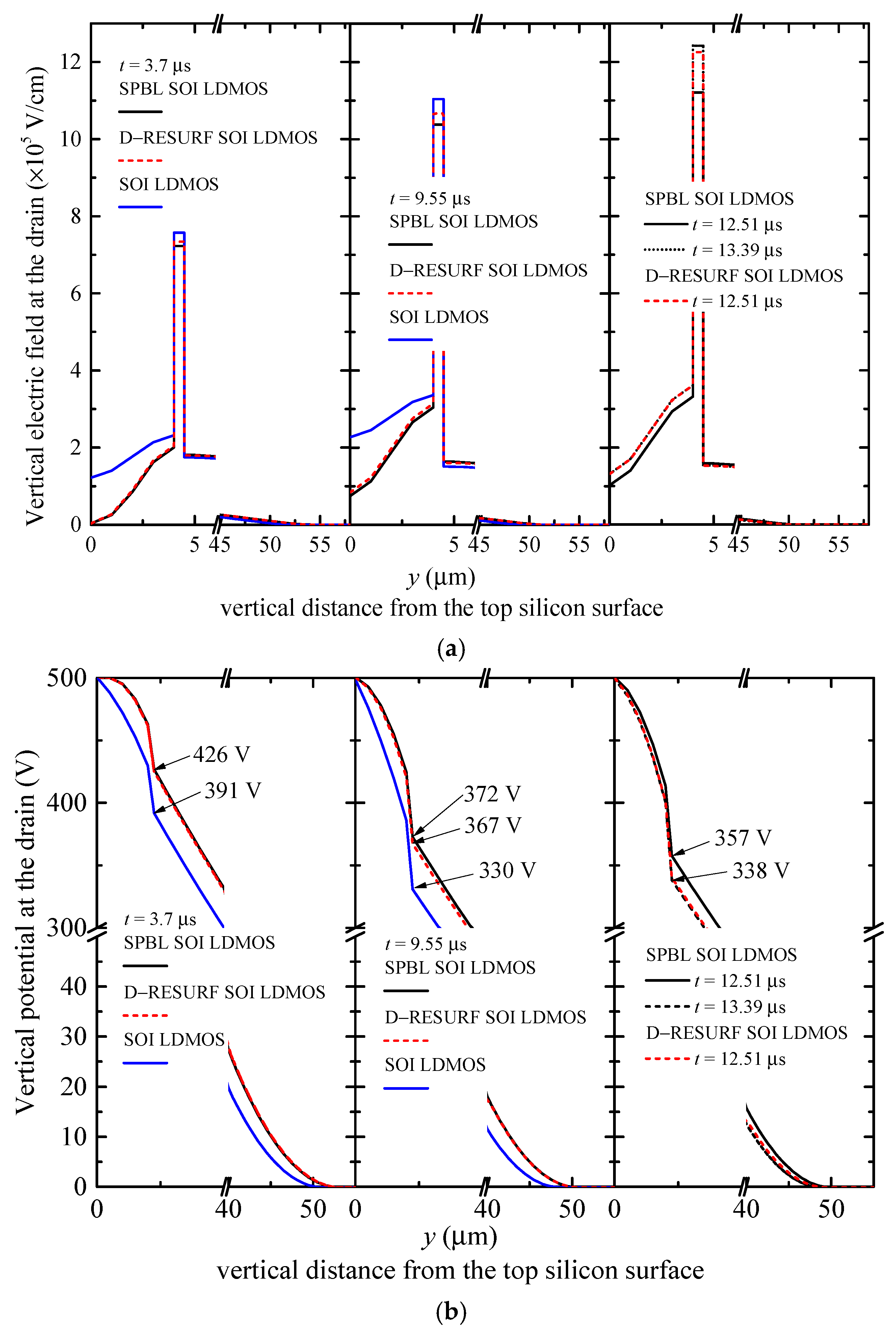
Figure 8 shows the distribution of the vertical electric field and potential at the drain of the three devices at different times for
T = 373 K and
Vd = 500 V. They were turned off at
t = 3.7 μs: the SOI LDMOS device was broken down first at
t = 9.55 μs, the D-RESURF SOI LDMOS device was broken down at
t = 12.51 μs, and the SPBL SOI LDMOS was broken down at
t = 13.39 μs. The
Tnonbv of the SPBL SOI LDMOS of 9.69 μs was 65.64% longer than that of the SOI LDMOS (5.85 μs), indicating that the operating frequency had a lower minimum and a wider range for the SPBL SOI LDMOS than the SOI LDMOS. The
Tnonbv of the D-RESURF SOI LDMOS was 8.81 μs, and it was slightly shorter than that of the SPBL SOI LDMOS. The vertical electric field in and the voltage sustained by the drift region and the BOX of the three devices were set to
E1 and
V1, respectively, and the voltage sustained by the substrate depletion layer was set to
V2.
Figure 8a shows that for a fixed time, the electric field at the vertical n+/n- junction at the drain of the SPBL SOI LDMOS was much lower than that of the SOI LDMOS because the
Nd of the SPBL SOI LDMOS was more than twice that of the SOI LDMOS. Solving the Poisson equation with boundary conditions shows that
E1 was lower for the SPBL SOI LDMOS than the SOI LDMOS. Therefore, for the same time and
Vd, the SPBL SOI LDMOS had a smaller
V1, a larger
V2, and a deeper substrate depletion layer than those of the SOI LDMOS. During device breakdown of the SPBL SOI LDMOS and SOI LDMOS, the maximum voltage sustained by the depletion layer and BOX and the substrate depletion layer depth were almost the same. Thus, the depletion layer of the SPBL SOI LDMOS was deeper than that of the SOI LDMOS during turn-off, and the depletion layer depth of both devices was equal during breakdown, such that the
Tnonbv of the SPBL SOI LDMOS was longer than that of the SOI LDMOS.
Figure 8b shows that at
t = 3.7 μs and
Vd = 500 V, the depth of the substrate depletion layer and
V1 were 52 μm and 74 V, respectively, for the SPBL SOI LDMOS. The depth of the substrate depletion layer and
V1 were 50 μm and 109 V, respectively, for the SOI LDMOS. At
t = 9.55 μs, the depth of the substrate depletion layer of the SPBL SOI LDMOS decreased to 49.5 μm,
V1 increased to 128 V, and the device was not broken down, whereas for the SOI LDMOS, the depth of the substrate depletion layer was 47.5 μm and
V1 increased to 170 V, which exceeded
StBV, resulting in device breakdown. Note that the
StBV of the device was higher at
T = 373 K than that at
T = 300 K. At
t = 13.39 μs, the depth of the substrate depletion layer of the SPBL SOI LDMOS decreased further to 48 μm,
V1 increased to 162 V, and the device was broken down. Because the
Nd of the D-RESURF SOI LDMOS was the same as that of the SPBL SOI LDMOS, their electric field and potential distribution were almost the same during turn-off and breakdown. The P-top layer in the D-RESURF SOI LDMOS not only weakened the electric field of the source but also enhanced the electric field of the drain. When the substrate depletion layer decreased, the
E1 of the D-RESURF SOI LDMOS increased faster than that of the SPBL SOI LDMOS. The D-RESURF SOI LDMOS was broken down earlier than the SPBL SOI LDMOS. The
Tnonbv of the D-RESURF SOI LDMOS was slightly shorter than that of the SPBL SOI LDMOS but longer than that of SOI LDMOS.


