Recent Advances in Tactile Sensing Technology


Abstract
:1. Introduction
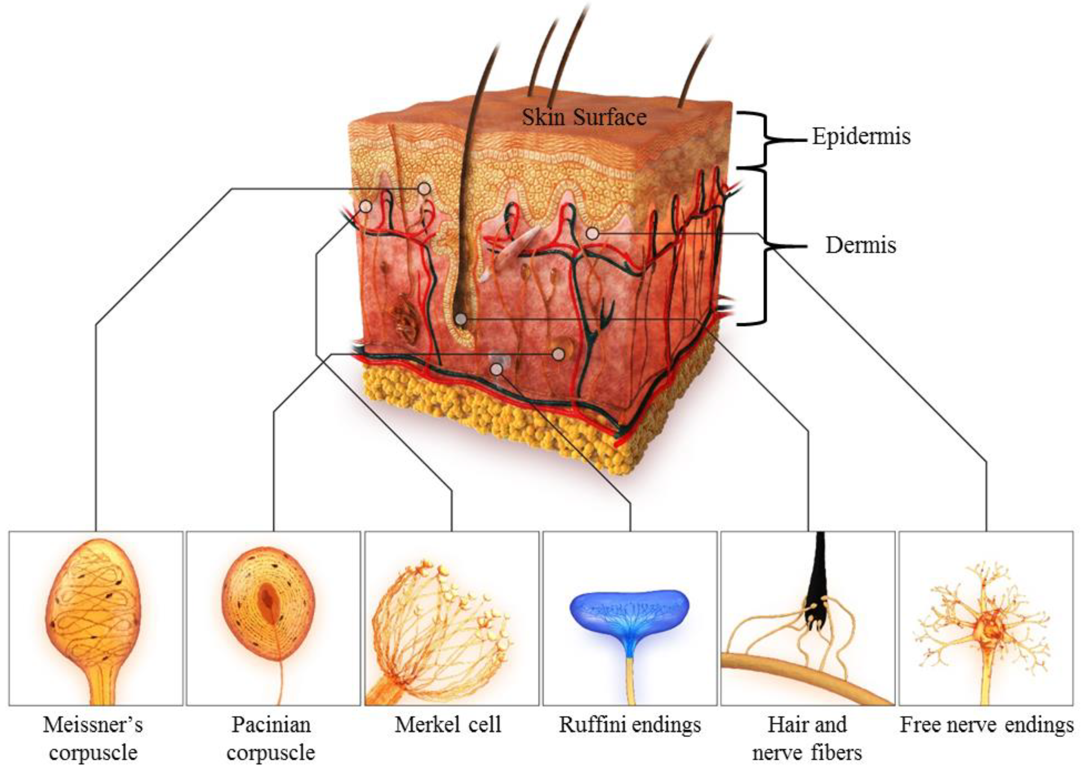
2. Fundamental Theories of Human Skin
3. Requirements for Tactile Sensing
3.1. High Sensitivity
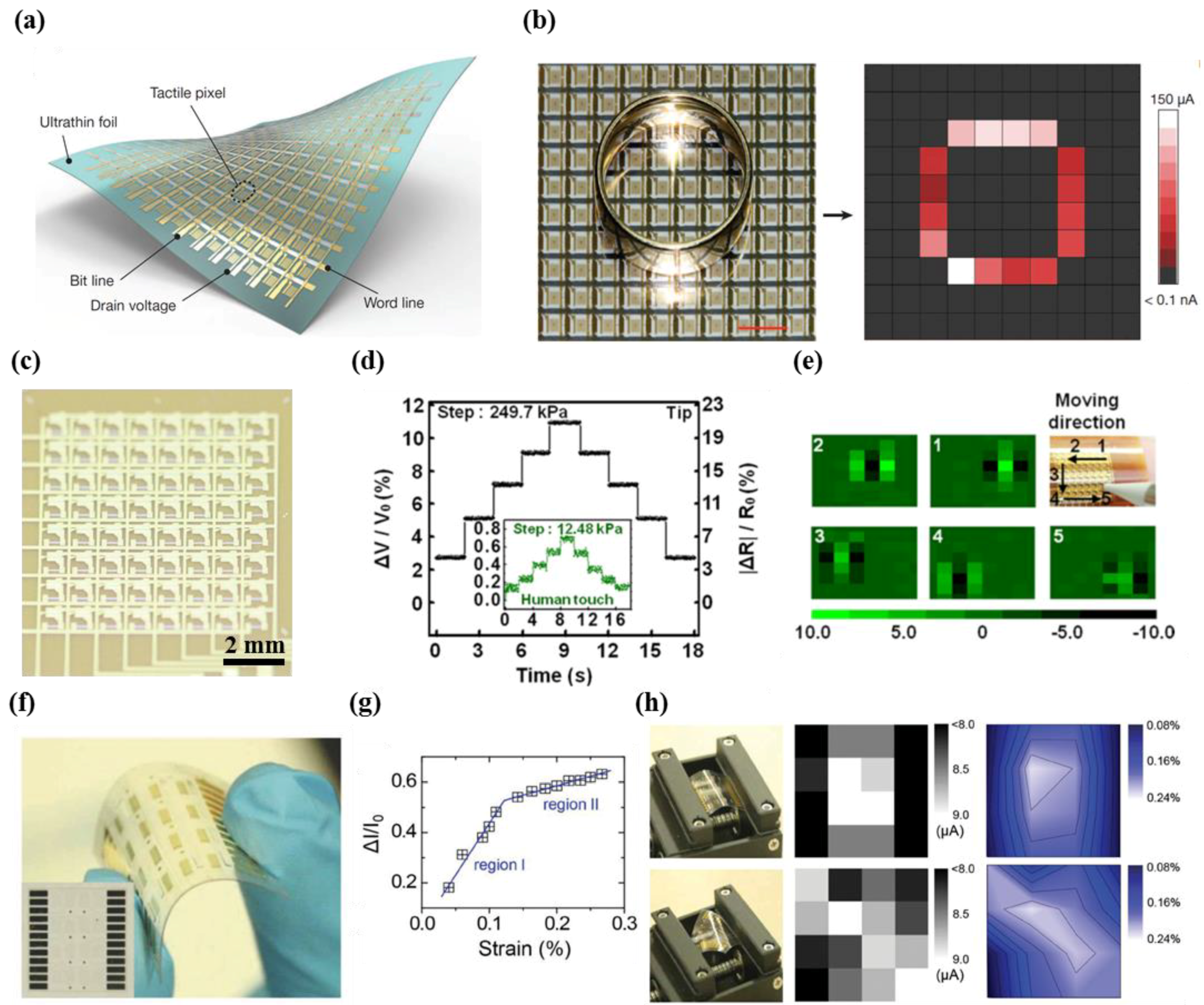
3.2. Active Matrix Circuitry
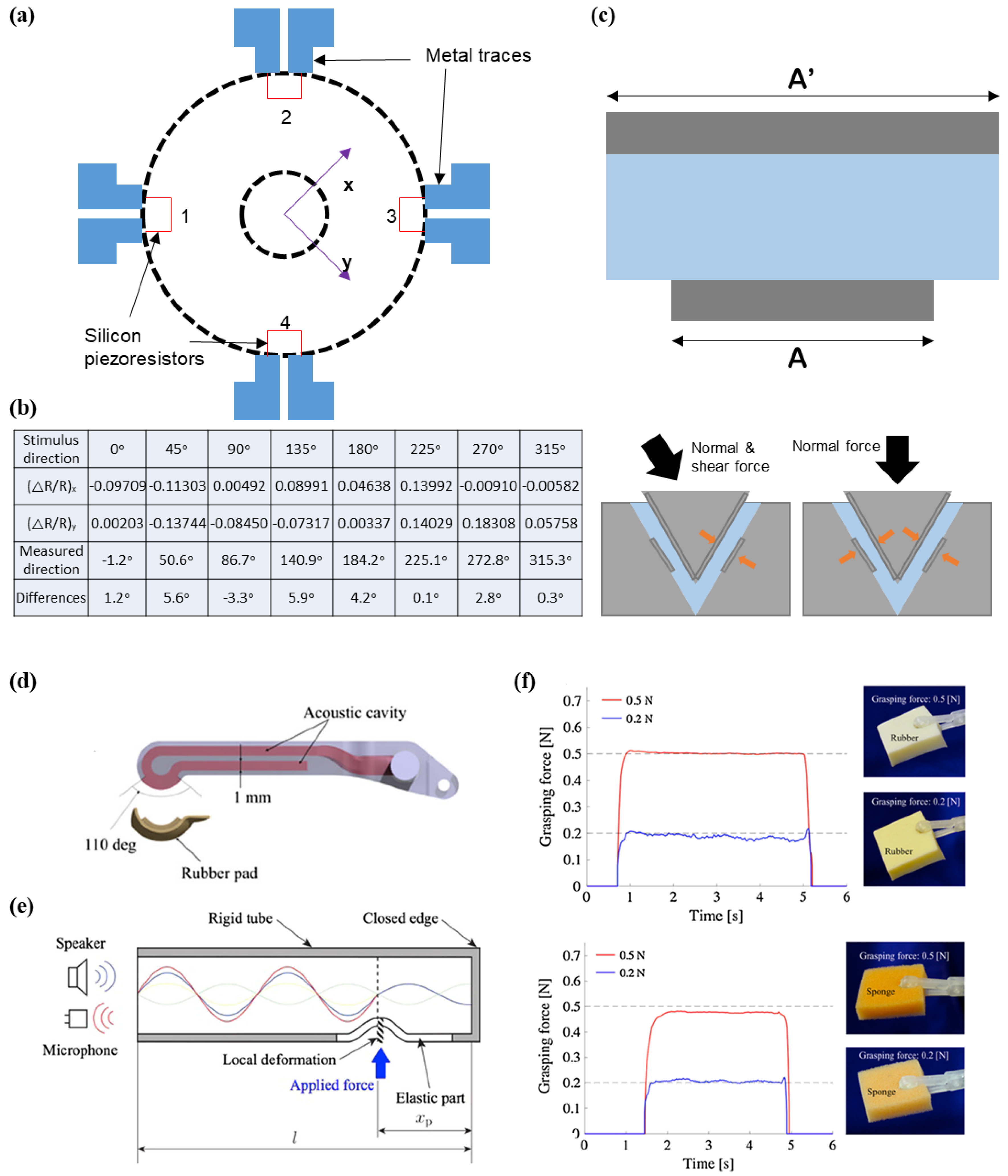
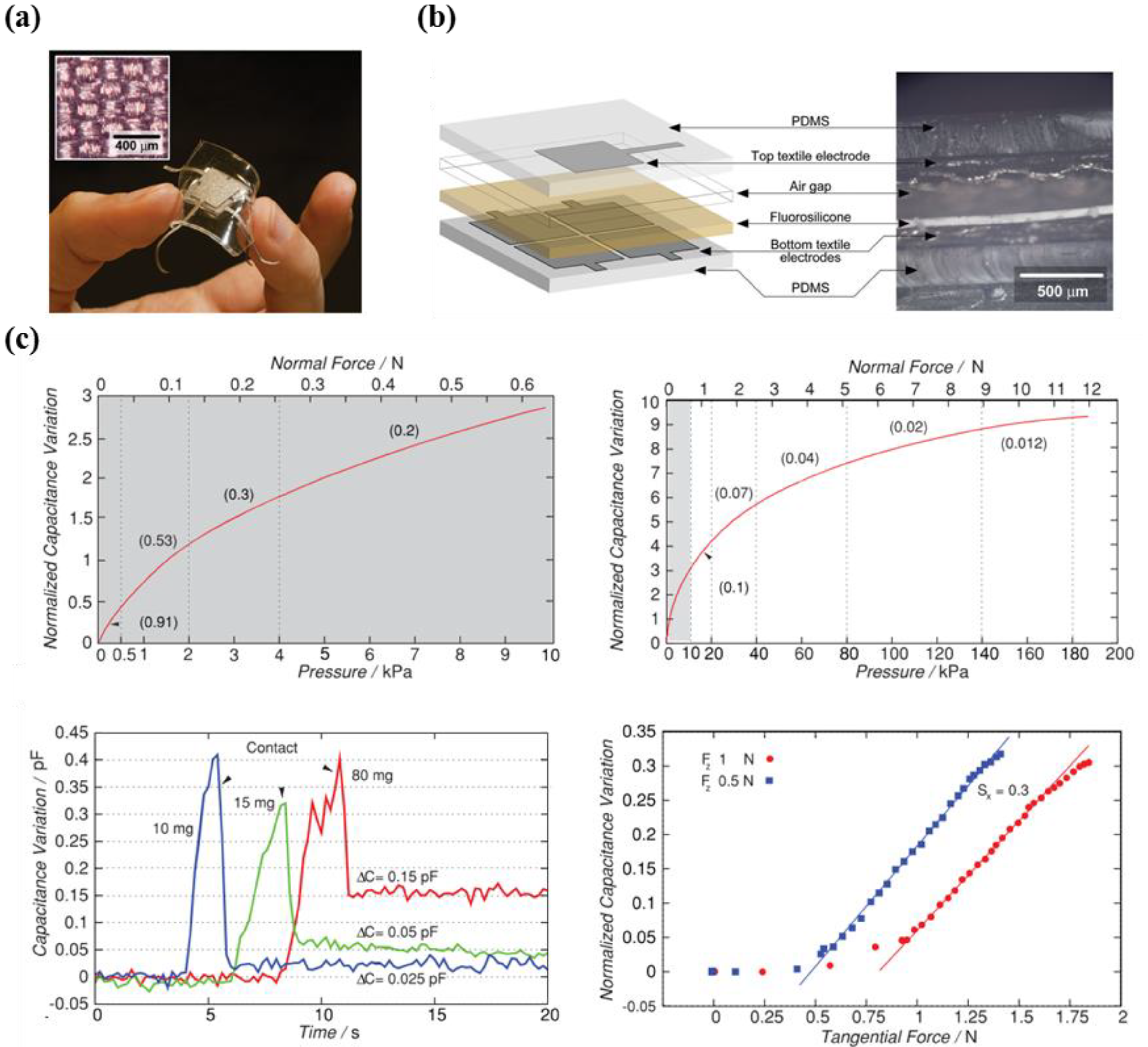
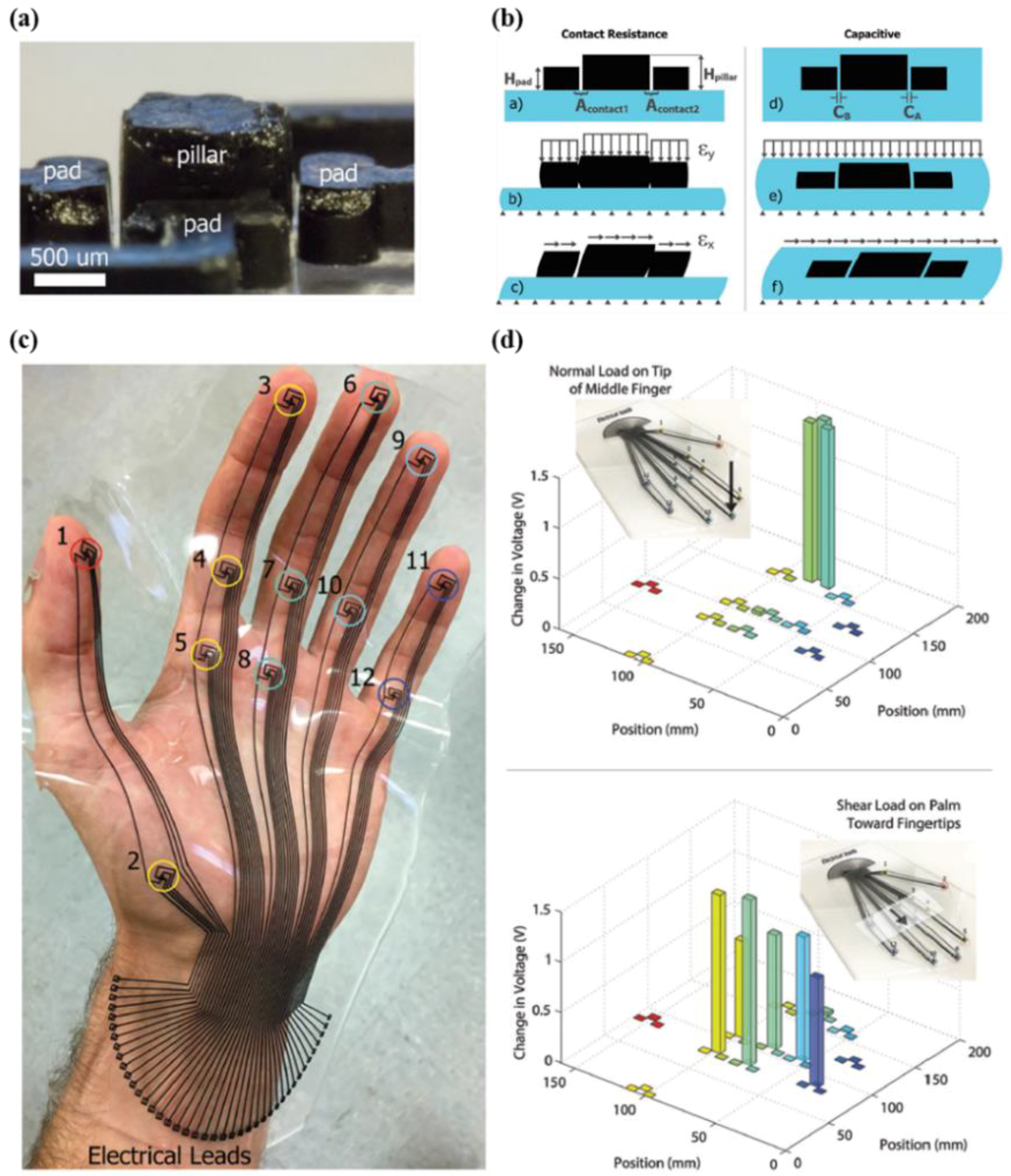
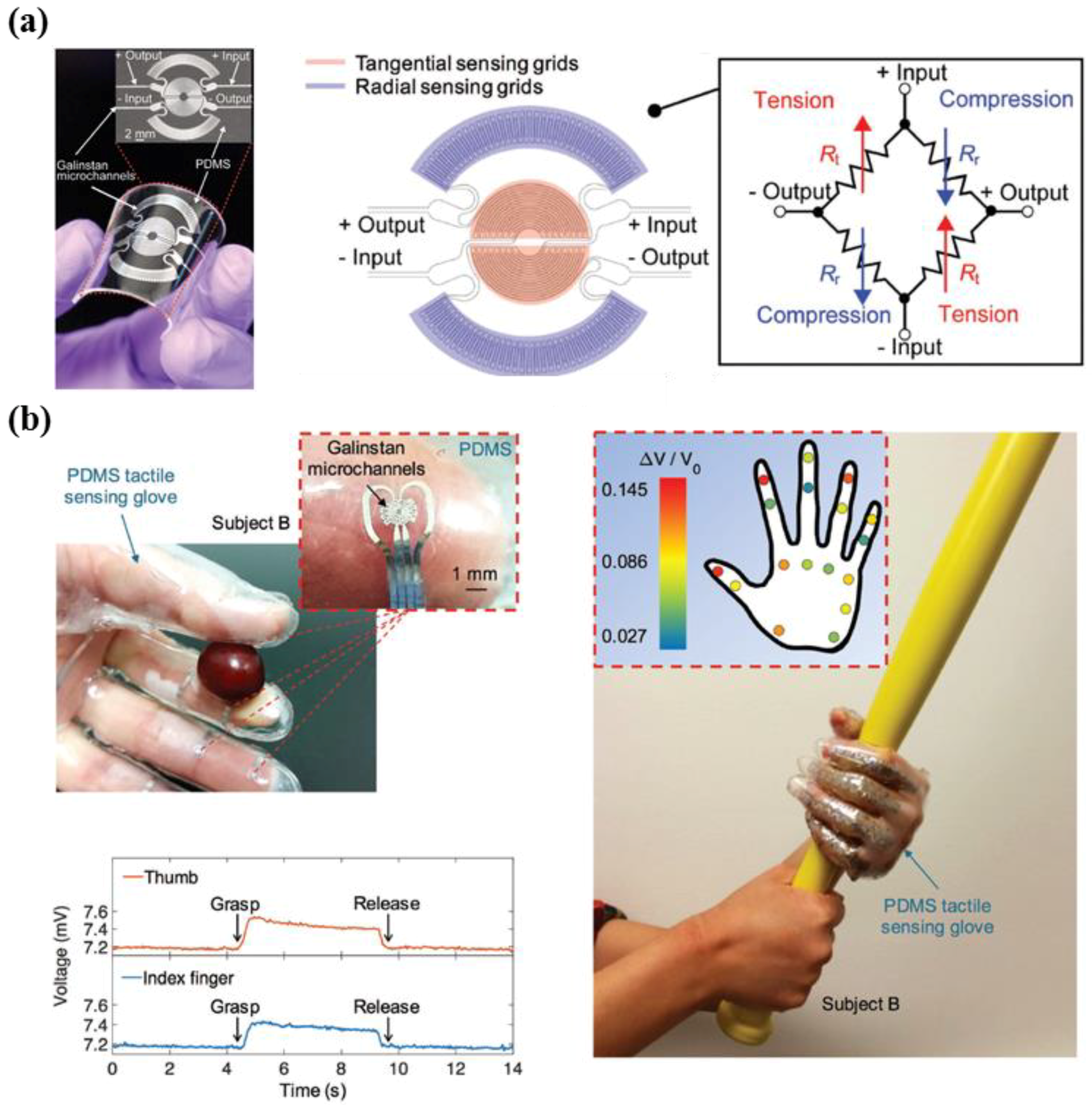
3.3. Shear Force Sensing
4. Novel Materials
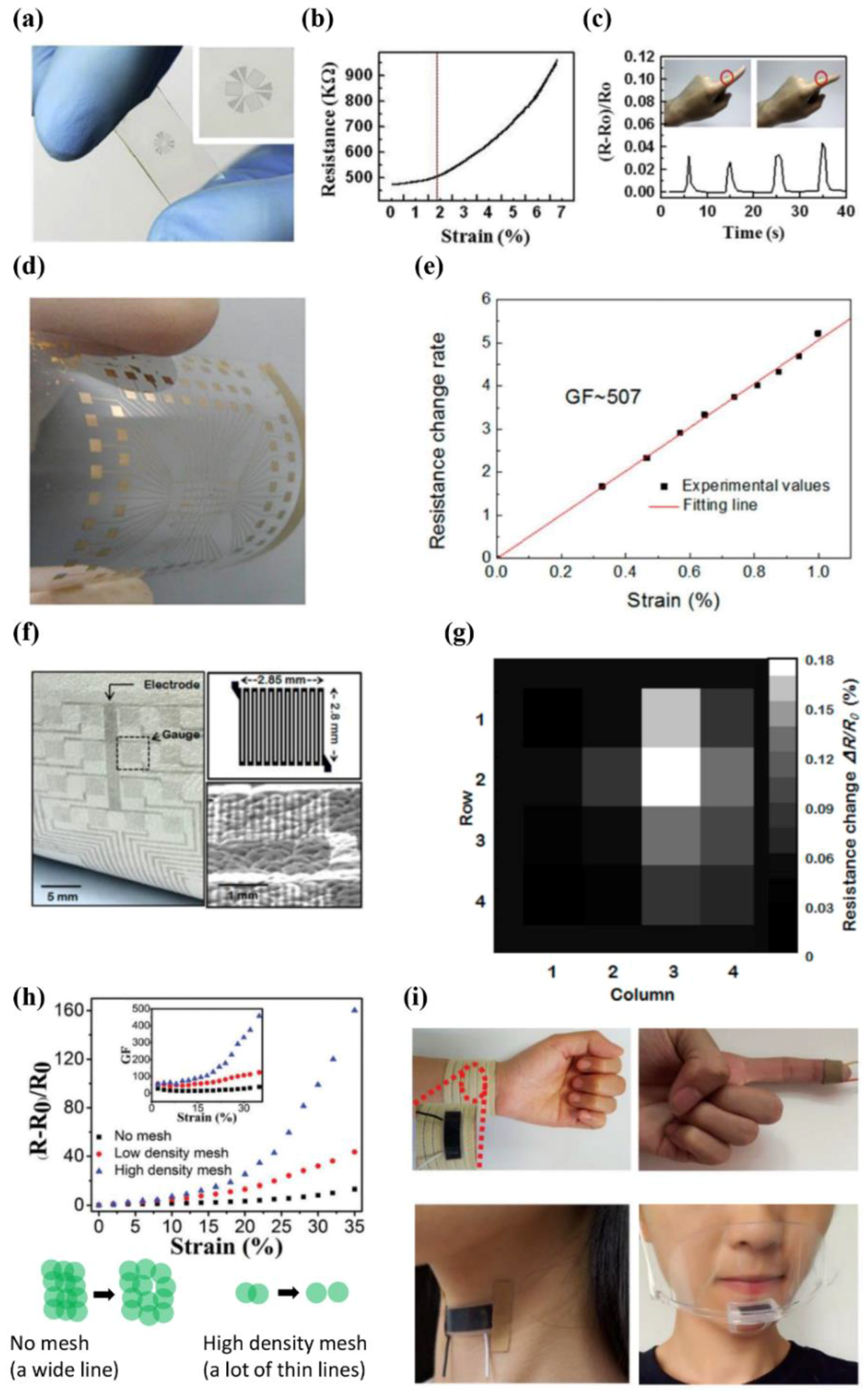
4.1. Single Crystalline Silicon
4.2. Graphene
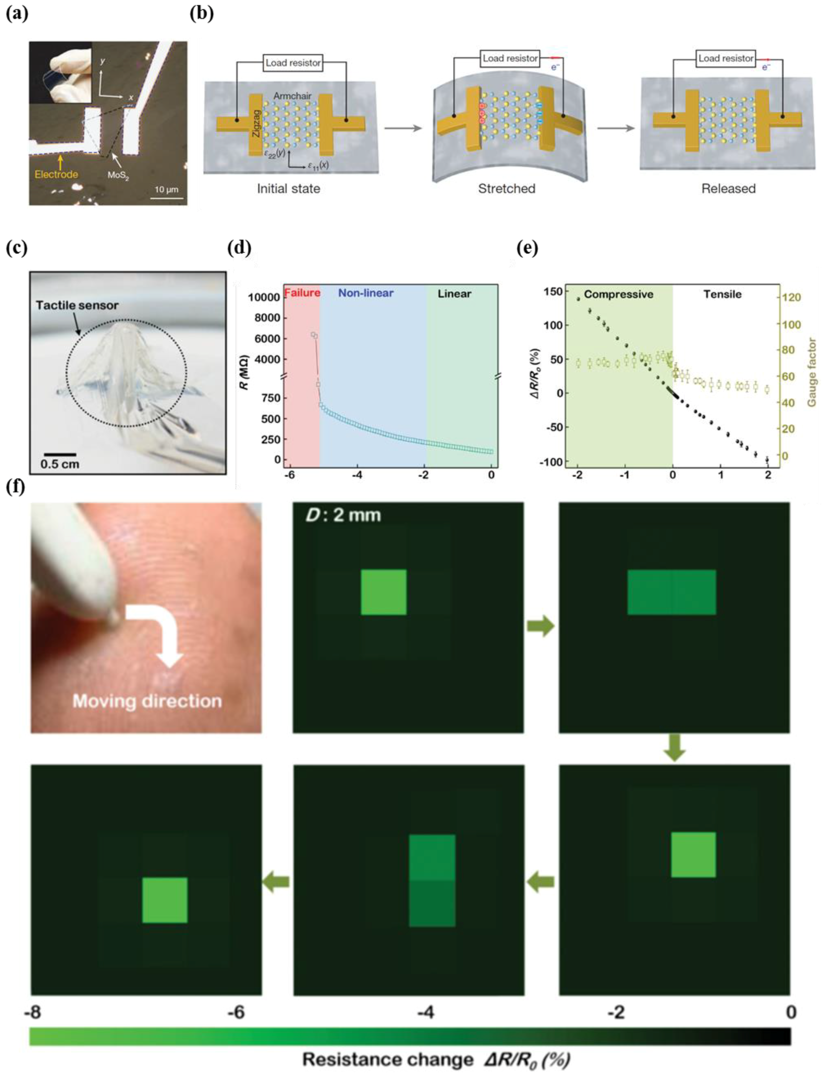
4.3. MoS2
5. Applications of Tactile Sensing
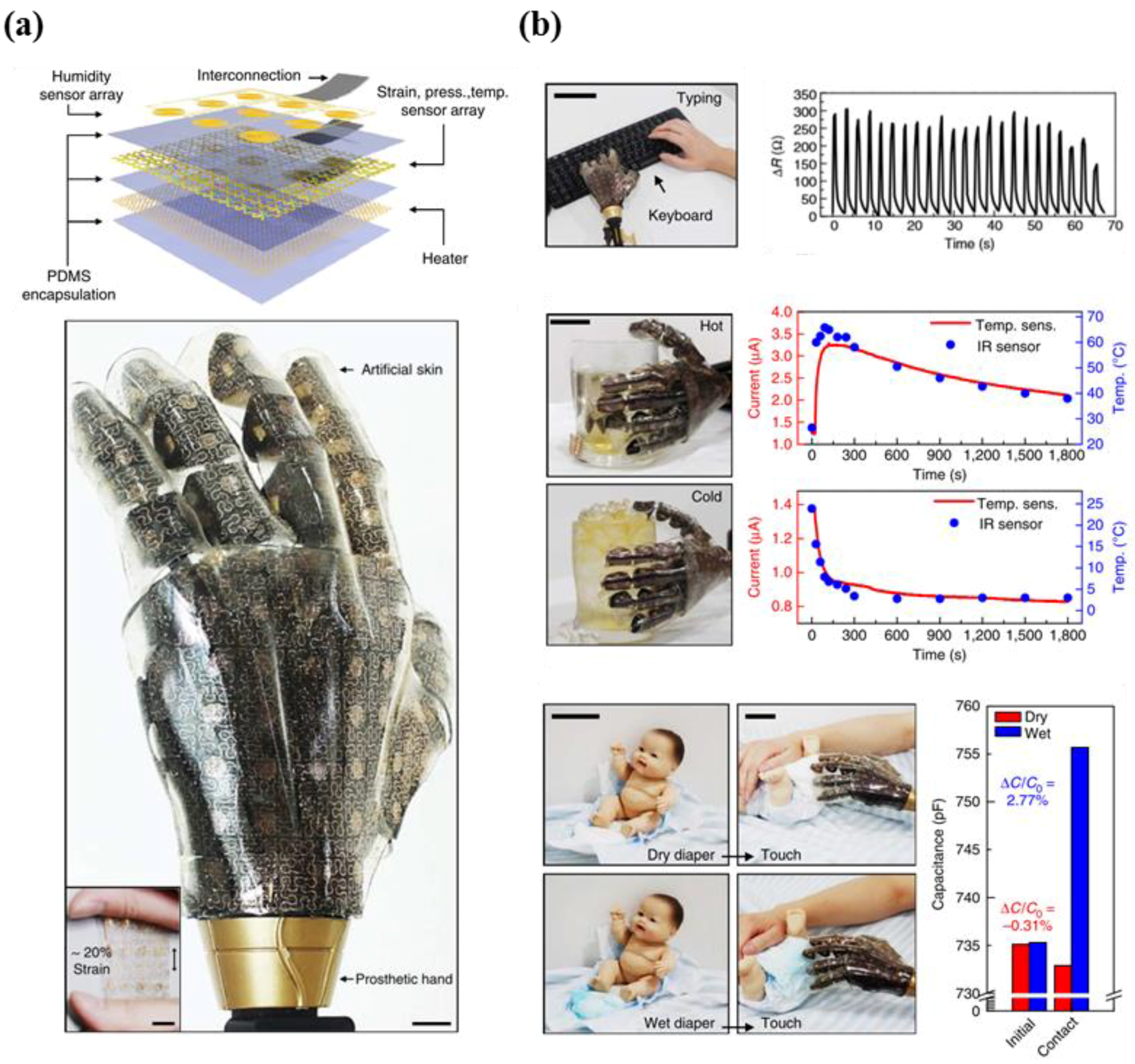
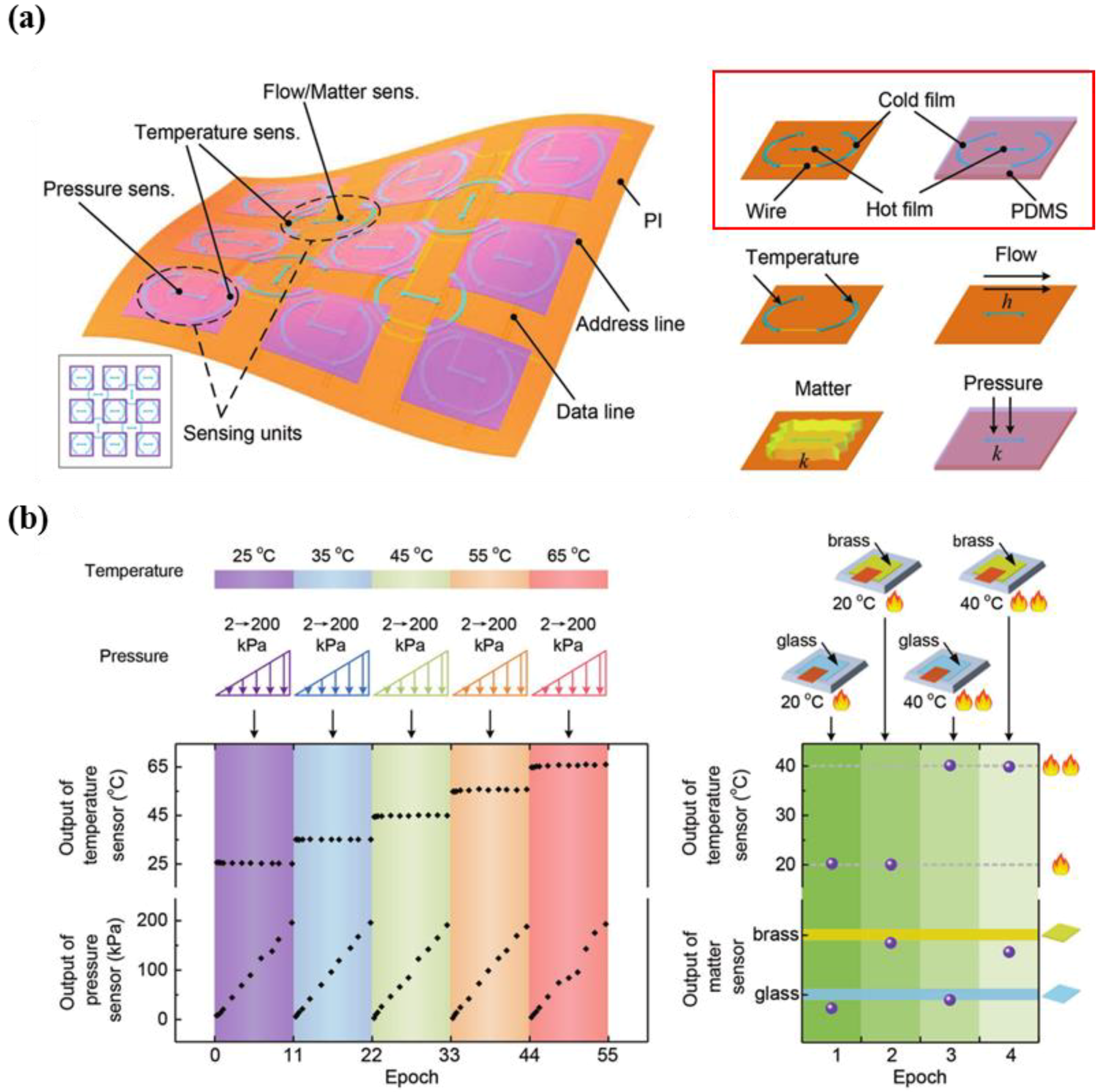
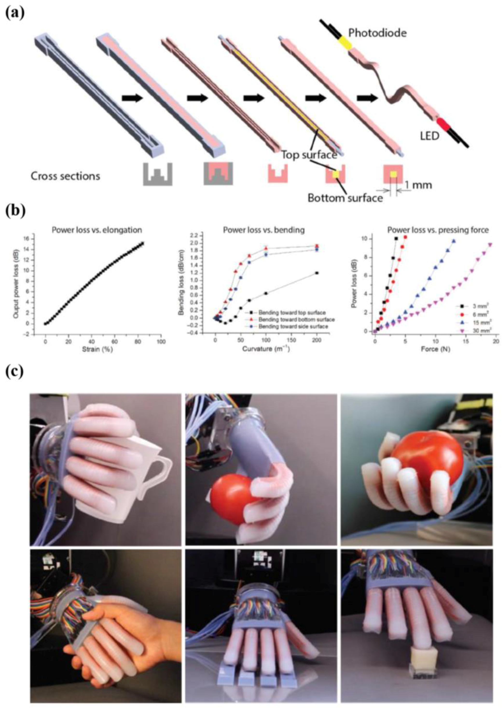
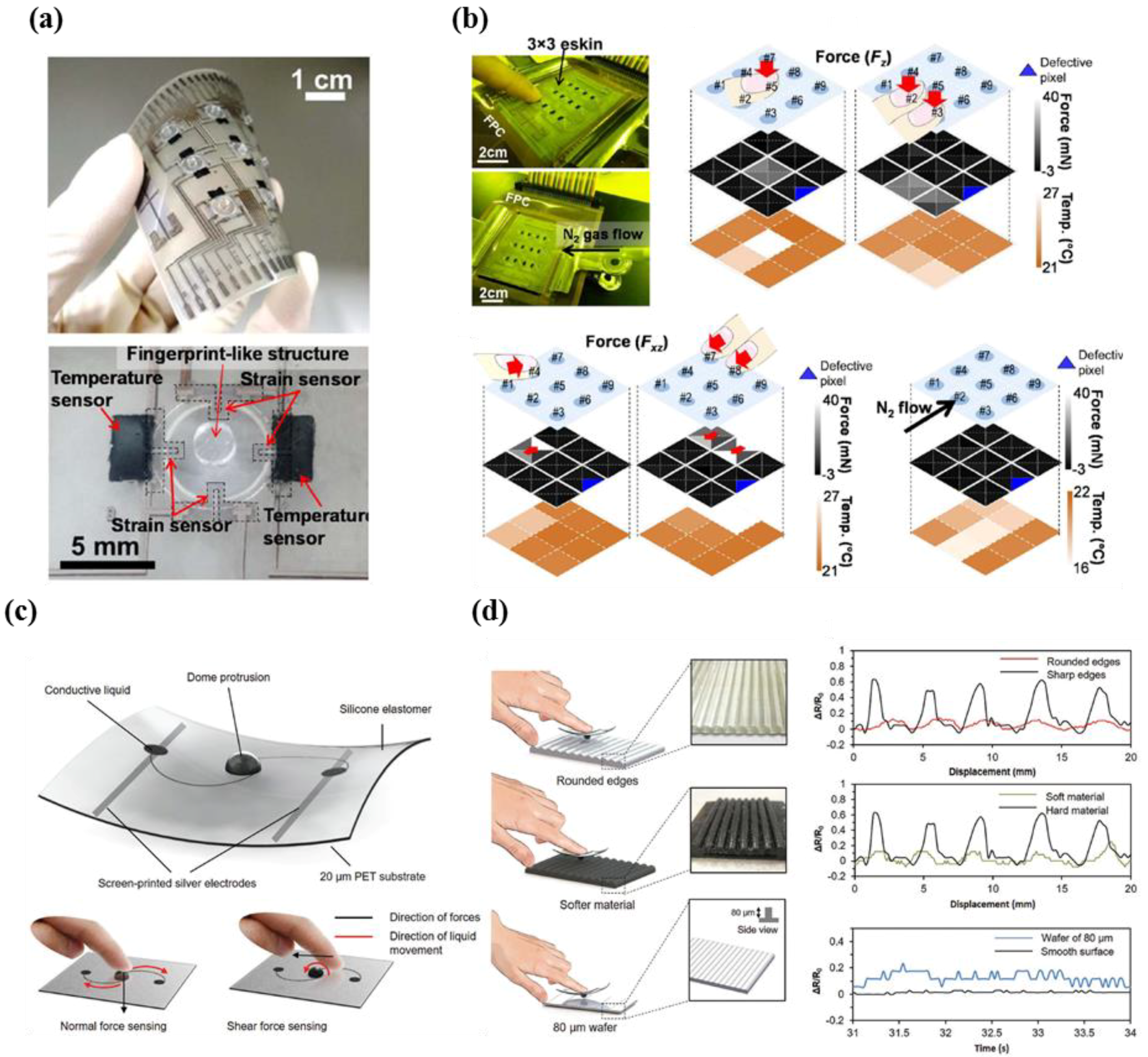
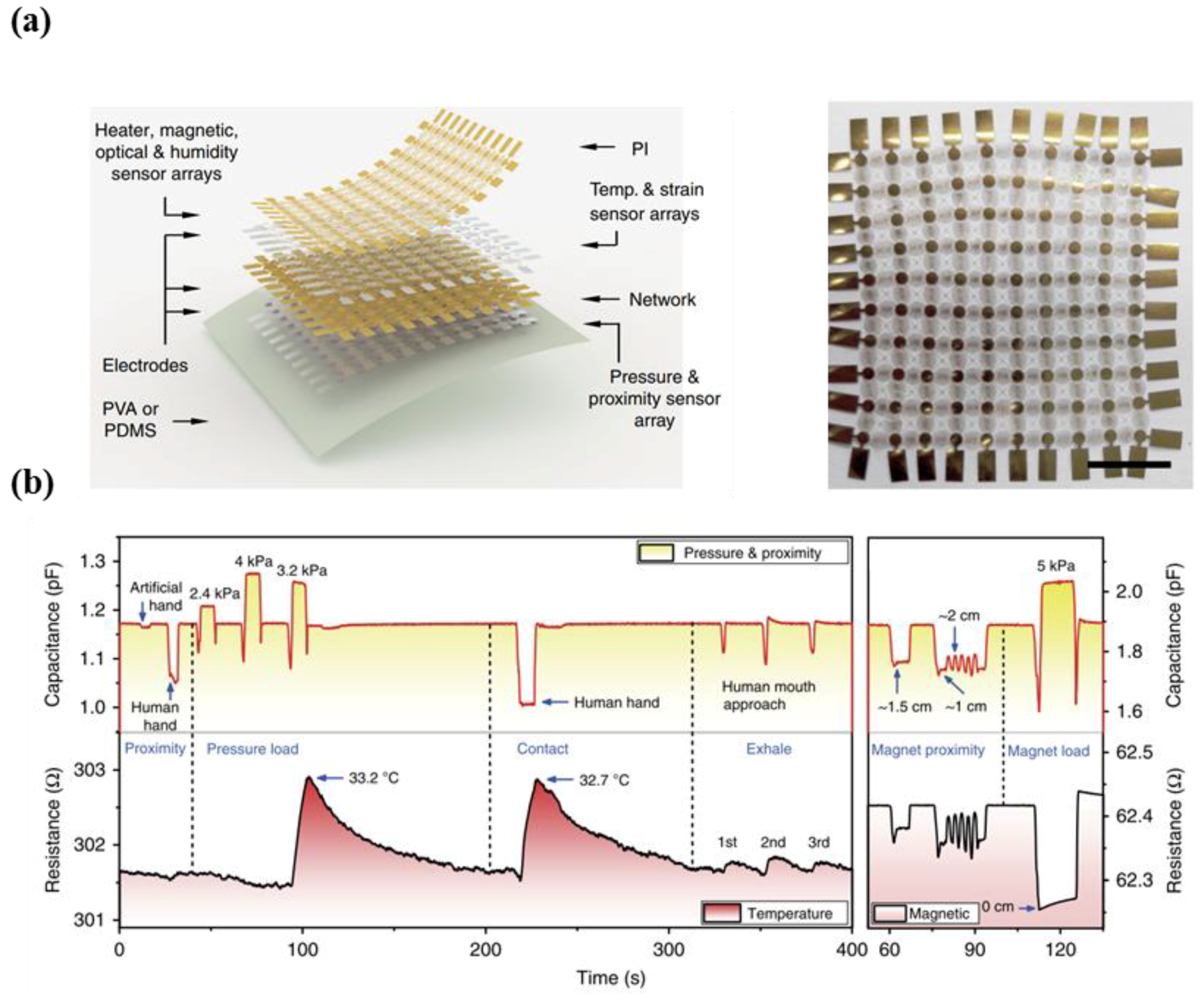
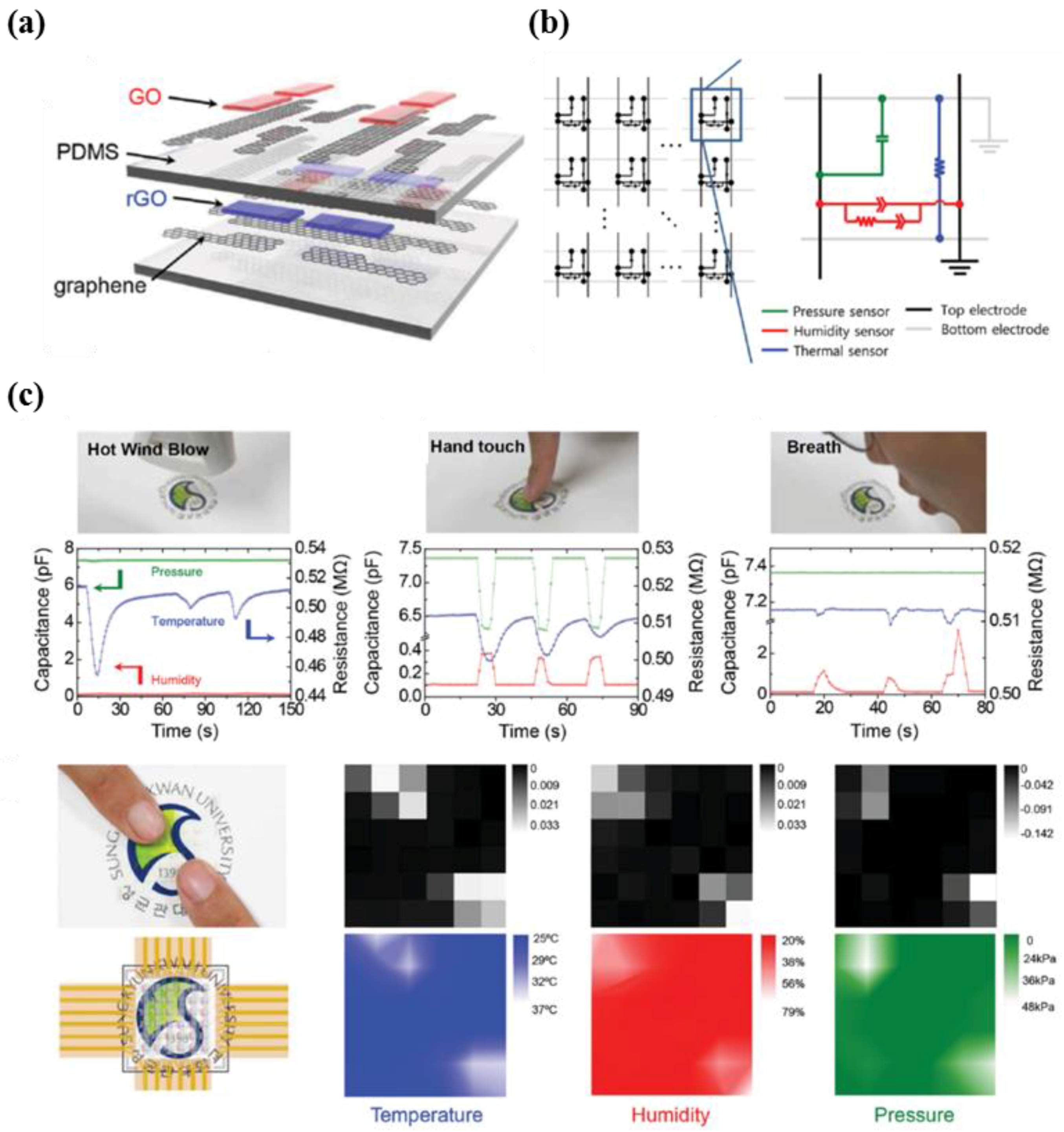
5.1. Multi-Functional E-Skin
5.2. Tactile Perception Analysis
5.3. Medical Forcep
6. Conclusions and Perspectives
Funding
Conflicts of Interest
References
- Büscher, G.H.; Kõiva, R.; Schürmann, C.; Haschke, R.; Ritter, H.J. Flexible and stretchable fabric-based tactile sensor. Robot. Auton. Syst. 2015, 63, 244–252. [Google Scholar] [CrossRef]
- De Maria, G.; Falco, P.; Natale, C.; Pirozzi, S. Integrated Force/Tactile Sensing: The Enabling Technology for Slipping Detection and Avoidance. In Proceedings of the IEEE International Conference on Robotics and Automation (ICRA), Seattle, WA, USA, 26–30 May 2015; pp. 3883–3889. [Google Scholar]
- Jamone, L.; Natale, L.; Metta, G.; Sandini, G. Highly sensitive soft tactile sensors for an anthropomorphic robotic hand. IEEE Sens. J. 2015, 15, 4226–4233. [Google Scholar] [CrossRef]
- Lee, H.; Park, K.; Kim, Y.; Kim, J. Durable and Repairable Soft Tactile Skin for Physical Human Robot Interaction. In Proceedings of the Companion of the 2017 ACM/IEEE International Conference on Human-Robot Interaction, Vienna, Austria, 6–9 March 2017; pp. 183–184. [Google Scholar]
- Pacchierotti, C.; Prattichizzo, D.; Kuchenbecker, K.J. Cutaneous feedback of fingertip deformation and vibration for palpation in robotic surgery. IEEE Trans. Biomed. Eng. 2016, 63, 278–287. [Google Scholar] [CrossRef] [PubMed]
- Romeo, R.A.; Oddo, C.M.; Carrozza, M.C.; Guglielmelli, E.; Zollo, L. Slippage detection with piezoresistive tactile sensors. Sensors 2017, 17, 1844. [Google Scholar] [CrossRef] [PubMed]
- Yuan, W.; Dong, S.; Adelson, E.H. Gelsight: High-resolution robot tactile sensors for estimating geometry and force. Sensors 2017, 17, 2762. [Google Scholar] [CrossRef] [PubMed]
- Zhang, T.; Jiang, L.; Wu, X.; Feng, W.; Zhou, D.; Liu, H. Fingertip three-axis tactile sensor for multifingered grasping. IEEE/ASME Trans. Mechatron. 2015, 20, 1875–1885. [Google Scholar] [CrossRef]
- Oddo, C.M.; Raspopovic, S.; Artoni, F.; Mazzoni, A.; Spigler, G.; Petrini, F.; Giambattistelli, F.; Vecchio, F.; Miraglia, F.; Zollo, L. Intraneural stimulation elicits discrimination of textural features by artificial fingertip in intact and amputee humans. eLife 2016, 5. [Google Scholar] [CrossRef] [PubMed]
- Raspopovic, S.; Capogrosso, M.; Petrini, F.M.; Bonizzato, M.; Rigosa, J.; Di Pino, G.; Carpaneto, J.; Controzzi, M.; Boretius, T.; Fernandez, E. Restoring natural sensory feedback in real-time bidirectional hand prostheses. Sci. Transl. Med. 2014, 6, 222ra219. [Google Scholar] [CrossRef] [PubMed]
- Son, D.; Lee, J.; Qiao, S.; Ghaffari, R.; Kim, J.; Lee, J.E.; Song, C.; Kim, S.J.; Lee, D.J.; Jun, S.W. Multifunctional wearable devices for diagnosis and therapy of movement disorders. Nat. Nanotechnol. 2014, 9, 397. [Google Scholar] [CrossRef] [PubMed]
- Won, S.M.; Kim, H.-S.; Lu, N.; Kim, D.-G.; Del Solar, C.; Duenas, T.; Ameen, A.; Rogers, J.A. Piezoresistive strain sensors and multiplexed arrays using assemblies of single-crystalline silicon nanoribbons on plastic substrates. IEEE Trans. Electron Devices 2011, 58, 4074–4078. [Google Scholar] [CrossRef]
- Ying, M.; Bonifas, A.P.; Lu, N.; Su, Y.; Li, R.; Cheng, H.; Ameen, A.; Huang, Y.; Rogers, J.A. Silicon nanomembranes for fingertip electronics. Nanotechnology 2012, 23, 344004. [Google Scholar] [CrossRef] [PubMed]
- Bae, S.-H.; Lee, Y.; Sharma, B.K.; Lee, H.-J.; Kim, J.-H.; Ahn, J.-H. Graphene-based transparent strain sensor. Carbon 2013, 51, 236–242. [Google Scholar] [CrossRef]
- Tao, L.-Q.; Wang, D.-Y.; Tian, H.; Ju, Z.-Y.; Liu, Y.; Pang, Y.; Chen, Y.-Q.; Yang, Y.; Ren, T.-L. Self-adapted and tunable graphene strain sensors for detecting both subtle and large human motions. Nanoscale 2017, 9, 8266–8273. [Google Scholar] [CrossRef] [PubMed]
- Zhao, J.; Wang, G.; Yang, R.; Lu, X.; Cheng, M.; He, C.; Xie, G.; Meng, J.; Shi, D.; Zhang, G. Tunable piezoresistivity of nanographene films for strain sensing. ACS Nano 2015, 9, 1622–1629. [Google Scholar] [CrossRef] [PubMed]
- Park, Y.J.; Lee, S.-K.; Kim, M.-S.; Kim, H.; Ahn, J.-H. Graphene-based conformal devices. ACS Nano 2014, 8, 7655–7662. [Google Scholar] [CrossRef] [PubMed]
- Park, M.; Park, Y.J.; Chen, X.; Park, Y.K.; Kim, M.S.; Ahn, J.H. MoS2-based tactile sensor for electronic skin applications. Adv. Mater. 2016, 28, 2556–2562. [Google Scholar] [CrossRef] [PubMed]
- Choi, Y.W.; Kang, D.; Pikhitsa, P.V.; Lee, T.; Kim, S.M.; Lee, G.; Tahk, D.; Choi, M. Ultra-sensitive pressure sensor based on guided straight mechanical cracks. Sci. Rep. 2017, 7, 40116. [Google Scholar] [CrossRef] [PubMed]
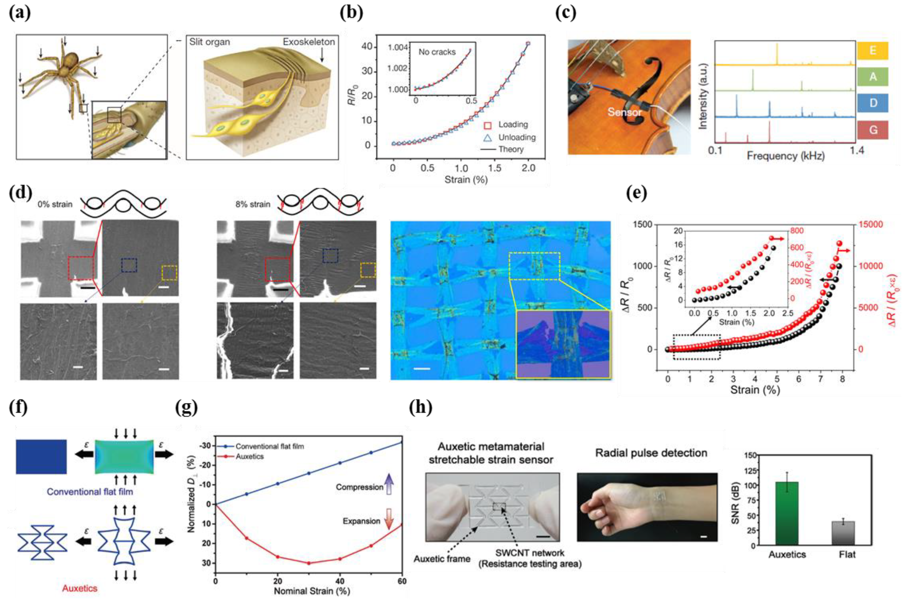
- Kang, D.; Pikhitsa, P.V.; Choi, Y.W.; Lee, C.; Shin, S.S.; Piao, L.; Park, B.; Suh, K.-Y.; Kim, T.-I.; Choi, M. Ultrasensitive mechanical crack-based sensor inspired by the spider sensory system. Nature 2014, 516, 222. [Google Scholar] [CrossRef] [PubMed]
- Lee, T.; Choi, Y.W.; Lee, G.; Kim, S.M.; Kang, D.; Choi, M. Crack-based strain sensor with diverse metal films by inserting an inter-layer. RSC Adv. 2017, 7, 34810–34815. [Google Scholar] [CrossRef] [Green Version]
- Yang, T.; Wang, W.; Zhang, H.; Li, X.; Shi, J.; He, Y.; Zheng, Q.-S.; Li, Z.; Zhu, H. Tactile sensing system based on arrays of graphene woven microfabrics: Electromechanical behavior and electronic skin application. ACS Nano 2015, 9, 10867–10875. [Google Scholar] [CrossRef] [PubMed]
- Pang, C.; Lee, G.-Y.; Kim, T.-I.; Kim, S.M.; Kim, H.N.; Ahn, S.-H.; Suh, K.-Y. A flexible and highly sensitive strain-gauge sensor using reversible interlocking of nanofibres. Nat. Mater. 2012, 11, 795–801. [Google Scholar] [CrossRef] [PubMed]
- Park, J.; Kim, M.; Lee, Y.; Lee, H.S.; Ko, H. Fingertip skin–inspired microstructured ferroelectric skins discriminate static/dynamic pressure and temperature stimuli. Sci. Adv. 2015, 1, e1500661. [Google Scholar] [CrossRef] [PubMed]
- Park, J.; Lee, Y.; Hong, J.; Ha, M.; Jung, Y.-D.; Lim, H.; Kim, S.Y.; Ko, H. Giant tunneling piezoresistance of composite elastomers with interlocked microdome arrays for ultrasensitive and multimodal electronic skins. ACS Nano 2014, 8, 4689–4697. [Google Scholar] [CrossRef] [PubMed]
- Park, J.; Lee, Y.; Hong, J.; Lee, Y.; Ha, M.; Jung, Y.; Lim, H.; Kim, S.Y.; Ko, H. Tactile-direction-sensitive and stretchable electronic skins based on human-skin-inspired interlocked microstructures. ACS Nano 2014, 8, 12020–12029. [Google Scholar] [CrossRef] [PubMed]
- Park, J.; Lee, Y.; Lim, S.; Lee, Y.; Jung, Y.; Lim, H.; Ko, H. Ultrasensitive piezoresistive pressure sensors based on interlocked micropillar arrays. BioNanoScience 2014, 4, 349–355. [Google Scholar] [CrossRef]
- Hammock, M.L.; Chortos, A.; Tee, B.C.; Tok, J.B.; Bao, Z. 25th anniversary article: The evolution of electronic skin (E-Skin): A brief history, design considerations, and recent progress. Adv. Mater. 2013, 25, 5997–6038. [Google Scholar] [CrossRef] [PubMed]
- Trung, T.Q.; Lee, N.E. Flexible and stretchable physical sensor integrated platforms for wearable human-activity monitoringand personal healthcare. Adv. Mater. 2016, 28, 4338–4372. [Google Scholar] [CrossRef] [PubMed]
- Yang, T.; Xie, D.; Li, Z.; Zhu, H. Recent advances in wearable tactile sensors: Materials, sensing mechanisms, and device performance. Mater. Sci. Eng. R Rep. 2017, 115, 1–37. [Google Scholar] [CrossRef]
- Rim, Y.S.; Bae, S.H.; Chen, H.; De Marco, N.; Yang, Y. Recent progress in materials and devices toward printable and flexible sensors. Adv. Mater. 2016, 28, 4415–4440. [Google Scholar] [CrossRef] [PubMed]
- Chortos, A.; Liu, J.; Bao, Z. Pursuing prosthetic electronic skin. Nat. Mater. 2016, 15, 937. [Google Scholar] [CrossRef] [PubMed]
- Dahiya, R.S.; Metta, G.; Valle, M.; Sandini, G. Tactile sensing—From humans to humanoids. IEEE Trans. Robot. 2010, 26, 1–20. [Google Scholar] [CrossRef]
- Dargahi, J.; Najarian, S. Human tactile perception as a standard for artificial tactile sensing—A review. Int. J. Med. Robot. Comput. Assist. Surg. 2004, 1, 23–35. [Google Scholar] [CrossRef] [PubMed]
- Girão, P.S.; Ramos, P.M.P.; Postolache, O.; Pereira, J.M.D. Tactile sensors for robotic applications. Measurement 2013, 46, 1257–1271. [Google Scholar] [CrossRef]
- Zimmerman, A.; Bai, L.; Ginty, D.D. The gentle touch receptors of mammalian skin. Science 2014, 346, 950–954. [Google Scholar] [CrossRef] [PubMed] [Green Version]
- Tee, B.C.-K.; Chortos, A.; Berndt, A.; Nguyen, A.K.; Tom, A.; McGuire, A.; Lin, Z.C.; Tien, K.; Bae, W.-G.; Wang, H. A skin-inspired organic digital mechanoreceptor. Science 2015, 350, 313–316. [Google Scholar] [CrossRef] [PubMed] [Green Version]
- Dellon, A.L.; Keller, K.M. Computer-assisted quantitative sensorimotor testing in patients with carpal and cubital tunnel syndromes. Ann. Plast. Surg. 1997, 38, 493–502. [Google Scholar] [CrossRef] [PubMed]
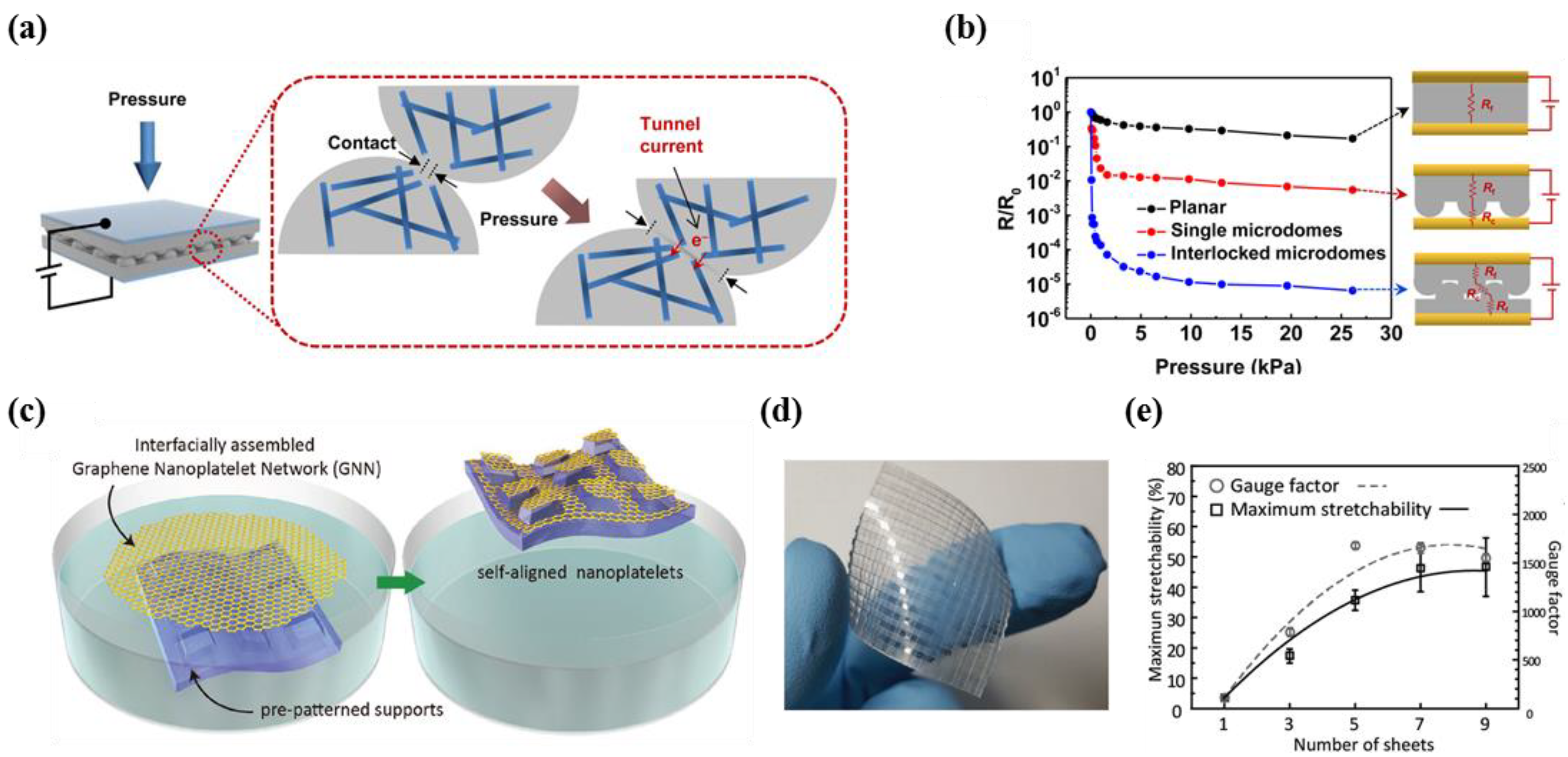
- Park, Y.; Shim, J.; Jeong, S.; Yi, G.R.; Chae, H.; Bae, J.W.; Kim, S.O.; Pang, C. Microtopography-guided conductive patterns of liquid-driven graphene nanoplatelet networks for stretchable and skin-conformal sensor array. Adv. Mater. 2017, 29. [Google Scholar] [CrossRef] [PubMed]
- Jiang, Y.; Liu, Z.; Matsuhisa, N.; Qi, D.; Leow, W.R.; Yang, H.; Yu, J.; Chen, G.; Liu, Y.; Wan, C. Auxetic mechanical metamaterials to enhance sensitivity of stretchable strain sensors. Adv. Mater. 2018, 30, 1706589. [Google Scholar] [CrossRef] [PubMed]
- Hu, W.; Niu, X.; Zhao, R.; Pei, Q. Elastomeric transparent capacitive sensors based on an interpenetrating composite of silver nanowires and polyurethane. Appl. Phys. Lett. 2013, 102, 38. [Google Scholar] [CrossRef]
- Kang, M.; Kim, J.; Jang, B.; Chae, Y.; Kim, J.-H.; Ahn, J.-H. Graphene-based three-dimensional capacitive touch sensor for wearable electronics. ACS Nano 2017, 11, 7950–7957. [Google Scholar] [CrossRef] [PubMed]
- Mannsfeld, S.C.; Tee, B.C.; Stoltenberg, R.M.; Chen, C.V.H.; Barman, S.; Muir, B.V.; Sokolov, A.N.; Reese, C.; Bao, Z. Highly sensitive flexible pressure sensors with microstructured rubber dielectric layers. Nat. Mater. 2010, 9, 859–864. [Google Scholar] [CrossRef] [PubMed]
- Metzger, C.; Fleisch, E.; Meyer, J.; Dansachmüller, M.; Graz, I.; Kaltenbrunner, M.; Keplinger, C.; Schwödiauer, R.; Bauer, S. Flexible-foam-based capacitive sensor arrays for object detection at low cost. Appl. Phys. Lett. 2008, 92, 013506. [Google Scholar] [CrossRef]
- Choi, M.; Jang, B.; Lee, W.; Lee, S.; Kim, T.W.; Lee, H.J.; Kim, J.H.; Ahn, J.H. Stretchable active matrix inorganic light-emitting diode display enabled by overlay-aligned roll-transfer printing. Adv. Funct. Mater. 2017, 27. [Google Scholar] [CrossRef]
- Choi, M.; Park, Y.J.; Sharma, B.K.; Bae, S.-R.; Kim, S.Y.; Ahn, J.-H. Flexible active-matrix organic light-emitting diode display enabled by MoS2 thin-film transistor. Sci. Adv. 2018, 4, eaas8721. [Google Scholar] [CrossRef] [PubMed]
- Larson, C.; Peele, B.; Li, S.; Robinson, S.; Totaro, M.; Beccai, L.; Mazzolai, B.; Shepherd, R. Highly stretchable electroluminescent skin for optical signaling and tactile sensing. Science 2016, 351, 1071–1074. [Google Scholar] [CrossRef] [PubMed]
- Sekitani, T.; Nakajima, H.; Maeda, H.; Fukushima, T.; Aida, T.; Hata, K.; Someya, T. Stretchable active-matrix organic light-emitting diode display using printable elastic conductors. Nat. Mater. 2009, 8, 494. [Google Scholar] [CrossRef] [PubMed]
- Kaltenbrunner, M.; Sekitani, T.; Reeder, J.; Yokota, T.; Kuribara, K.; Tokuhara, T.; Drack, M.; Schwödiauer, R.; Graz, I.; Bauer-Gogonea, S. An ultra-lightweight design for imperceptible plastic electronics. Nature 2013, 499, 458. [Google Scholar] [CrossRef] [PubMed]
- Nela, L.; Tang, J.; Cao, Q.; Tulevski, G.; Han, S.-J. Large-area high-performance flexible pressure sensor with carbon nanotube active matrix for electronic skin. Nano Lett. 2018, 18, 2054–2059. [Google Scholar] [CrossRef] [PubMed]
- Park, M.; Kim, M.-S.; Park, Y.-K.; Ahn, J.-H. Si membrane based tactile sensor with active matrix circuitry for artificial skin applications. Appl. Phys. Lett. 2015, 106, 043502. [Google Scholar] [CrossRef]
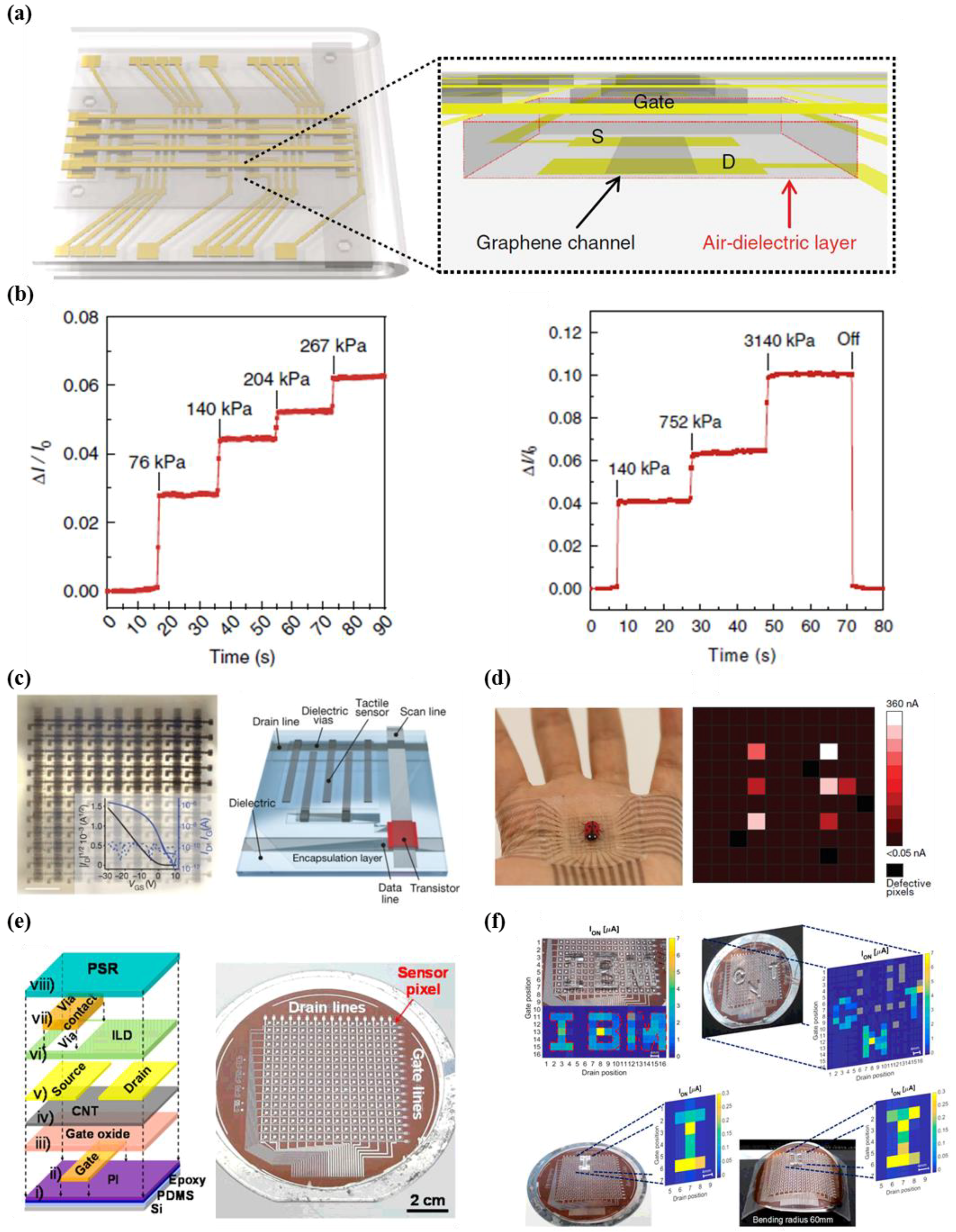
- Shin, S.-H.; Ji, S.; Choi, S.; Pyo, K.-H.; An, B.W.; Park, J.; Kim, J.; Kim, J.-Y.; Lee, K.-S.; Kwon, S.-Y. Integrated arrays of air-dielectric graphene transistors as transparent active-matrix pressure sensors for wide pressure ranges. Nat. Commun. 2017, 8, 14950. [Google Scholar] [CrossRef] [PubMed]
- Someya, T.; Kato, Y.; Sekitani, T.; Iba, S.; Noguchi, Y.; Murase, Y.; Kawaguchi, H.; Sakurai, T. Conformable, flexible, large-area networks of pressure and thermal sensors with organic transistor active matrixes. Proc. Nat. Acad. Sci. USA 2005, 102, 12321–12325. [Google Scholar] [CrossRef] [PubMed] [Green Version]
- Sun, Q.; Seung, W.; Kim, B.J.; Seo, S.; Kim, S.W.; Cho, J.H. Active matrix electronic skin strain sensor based on piezopotential-powered graphene transistors. Adv. Mater. 2015, 27, 3411–3417. [Google Scholar] [CrossRef] [PubMed]
- Takahashi, T.; Takei, K.; Gillies, A.G.; Fearing, R.S.; Javey, A. Carbon nanotube active-matrix backplanes for conformal electronics and sensors. Nano Lett. 2011, 11, 5408–5413. [Google Scholar] [CrossRef] [PubMed]
- Takei, K.; Takahashi, T.; Ho, J.C.; Ko, H.; Gillies, A.G.; Leu, P.W.; Fearing, R.S.; Javey, A. Nanowire active-matrix circuitry for low-voltage macroscale artificial skin. Nat. Mater. 2010, 9, 821–826. [Google Scholar] [CrossRef] [PubMed]
- Wang, C.; Hwang, D.; Yu, Z.; Takei, K.; Park, J.; Chen, T.; Ma, B.; Javey, A. User-interactive electronic skin for instantaneous pressure visualization. Nat. Mater. 2013, 12, 899. [Google Scholar] [CrossRef] [PubMed]
- Wang, S.; Xu, J.; Wang, W.; Wang, G.-J.N.; Rastak, R.; Molina-Lopez, F.; Chung, J.W.; Niu, S.; Feig, V.R.; Lopez, J. Skin electronics from scalable fabrication of an intrinsically stretchable transistor array. Nature 2018, 555, 83. [Google Scholar] [CrossRef] [PubMed]
- Yeom, C.; Chen, K.; Kiriya, D.; Yu, Z.; Cho, G.; Javey, A. Large-area compliant tactile sensors using printed carbon nanotube active-matrix backplanes. Adv. Mater. 2015, 27, 1561–1566. [Google Scholar] [CrossRef] [PubMed]
- Yousef, H.; Boukallel, M.; Althoefer, K. Tactile sensing for dexterous in-hand manipulation in robotics—A review. Sens. Actuators A Phys. 2011, 167, 171–187. [Google Scholar] [CrossRef]
- Engel, J.; Chen, J.; Liu, C. Development of polyimide flexible tactile sensor skin. J. Micromech. Microeng. 2003, 13, 359. [Google Scholar] [CrossRef]
- Hwang, E.-S.; Seo, J.-H.; Kim, Y.-J. A polymer-based flexible tactile sensor for both normal and shear load detections and its application for robotics. Microelectromech. Syst. J. 2007, 16, 556–563. [Google Scholar] [CrossRef]
- Lee, H.-K.; Chung, J.; Chang, S.-I.; Yoon, E. Normal and shear force measurement using a flexible polymer tactile sensor with embedded multiple capacitors. Microelectromech. Syst. J. 2008, 17, 934–942. [Google Scholar]
- Cheng, M.-Y.; Lin, C.-L.; Lai, Y.-T.; Yang, Y.-J. A polymer-based capacitive sensing array for normal and shear force measurement. Sensors 2010, 10, 10211–10225. [Google Scholar] [CrossRef] [PubMed]
- Hu, C.-F.; Su, W.-S.; Fang, W. Development of patterned carbon nanotubes on a 3d polymer substrate for the flexible tactile sensor application. J. Micromech. Microeng. 2011, 21, 115012. [Google Scholar] [CrossRef]
- Lee, H.-K.; Chung, J.; Chang, S.-I.; Yoon, E. Real-time measurement of the three-axis contact force distribution using a flexible capacitive polymer tactile sensor. J. Micromech. Microeng. 2011, 21, 035010. [Google Scholar] [CrossRef]
- Harada, S.; Kanao, K.; Yamamoto, Y.; Arie, T.; Akita, S.; Takei, K. Fully printed flexible fingerprint-like three-axis tactile and slip force and temperature sensors for artificial skin. ACS Nano 2014, 8, 12851–12857. [Google Scholar] [CrossRef] [PubMed]
- Viry, L.; Levi, A.; Totaro, M.; Mondini, A.; Mattoli, V.; Mazzolai, B.; Beccai, L. Flexible three-axial force sensor for soft and highly sensitive artificial touch. Adv. Mater. 2014, 26, 2659–2664. [Google Scholar] [CrossRef] [PubMed]
- Jung, Y.; Lee, D.-G.; Park, J.; Ko, H.; Lim, H. Piezoresistive tactile sensor discriminating multidirectional forces. Sensors 2015, 15, 25463–25473. [Google Scholar] [CrossRef] [PubMed]
- Yu, P.; Liu, W.; Gu, C.; Cheng, X.; Fu, X. Flexible piezoelectric tactile sensor array for dynamic three-axis force measurement. Sensors 2016, 16, 819. [Google Scholar] [CrossRef] [PubMed]
- Charalambides, A.; Bergbreiter, S. Rapid manufacturing of mechanoreceptive skins for slip detection in robotic grasping. Adv. Mater. Technol. 2017, 2. [Google Scholar] [CrossRef]
- Yeo, J.C.; Liu, Z.; Zhang, Z.Q.; Zhang, P.; Wang, Z.; Lim, C.T. Wearable mechanotransduced tactile sensor for haptic perception. Adv. Mater. Technol. 2017, 2. [Google Scholar] [CrossRef]
- Chen, X.; Shao, J.; Tian, H.; Li, X.; Tian, Y.; Wang, C. Flexible three-axial tactile sensors with microstructure-enhanced piezoelectric effect and specially-arranged piezoelectric arrays. Smart Mater. Struct. 2018, 27. [Google Scholar] [CrossRef]
- Lee, W.; Jang, H.; Jang, B.; Kim, J.H.; Ahn, J.H. Stretchable SI logic devices with graphene interconnects. Small 2015, 11, 6272–6277. [Google Scholar] [CrossRef] [PubMed]
- Khang, D.-Y.; Jiang, H.; Huang, Y.; Rogers, J.A. A stretchable form of single-crystal silicon for high-performance electronics on rubber substrates. Science 2006, 311, 208–212. [Google Scholar] [CrossRef] [PubMed]
- Kim, D.H.; Yoo, H.G.; Hong, S.M.; Jang, B.; Park, D.Y.; Joe, D.J.; Kim, J.H.; Lee, K.J. Simultaneous roll transfer and interconnection of flexible silicon nand flash memory. Adv. Mater. 2016, 28, 8371–8378. [Google Scholar] [CrossRef] [PubMed]
- Li, N.; Bedell, S.; Hu, H.; Han, S.J.; Liu, X.H.; Saenger, K.; Sadana, D. Single crystal flexible electronics enabled by 3D spalling. Adv. Mater. 2017, 29. [Google Scholar] [CrossRef] [PubMed]
- Jang, J.-S.; Kang, T.-H.; Song, H.-W.; Park, Y.-K.; Kim, M.-S. High-performance multimodal flexible tactile sensor capable of measuring pressure and temperature simultaneously. J. Korean Soc. Precis. Eng. 2014, 31, 683–688. [Google Scholar] [CrossRef]
- Hwang, S.-W.; Tao, H.; Kim, D.-H.; Cheng, H.; Song, J.-K.; Rill, E.; Brenckle, M.A.; Panilaitis, B.; Won, S.M.; Kim, Y.-S. A physically transient form of silicon electronics. Science 2012, 337, 1640–1644. [Google Scholar] [CrossRef] [PubMed]
- Yu, K.J.; Kuzum, D.; Hwang, S.-W.; Kim, B.H.; Juul, H.; Kim, N.H.; Won, S.M.; Chiang, K.; Trumpis, M.; Richardson, A.G. Bioresorbable silicon electronics for transient spatiotemporal mapping of electrical activity from the cerebral cortex. Nat. Mater. 2016, 15, 782. [Google Scholar] [CrossRef] [PubMed]
- Menard, E.; Lee, K.; Khang, D.-Y.; Nuzzo, R.; Rogers, J. A printable form of silicon for high performance thin film transistors on plastic substrates. Appl. Phys. Lett. 2004, 84, 5398–5400. [Google Scholar] [CrossRef]
- Menard, E.; Nuzzo, R.G.; Rogers, J.A. Bendable single crystal silicon thin film transistors formed by printing on plastic substrates. Appl. Phys. Lett. 2005, 86, 093507. [Google Scholar] [CrossRef]
- Lee, K.J.; Motala, M.J.; Meitl, M.A.; Childs, W.R.; Menard, E.; Shim, A.K.; Rogers, J.A.; Nuzzo, R.G. Large-area, selective transfer of microstructured silicon: A printing-based approach to high-performance thin-film transistors supported on flexible substrates. Adv. Mater. 2005, 17, 2332–2336. [Google Scholar] [CrossRef]
- Yuan, H.-C.; Ma, Z.; Roberts, M.M.; Savage, D.E.; Lagally, M.G. High-speed strained-single-crystal-silicon thin-film transistors on flexible polymers. J. Appl. Phys. 2006, 100, 013708. [Google Scholar] [CrossRef]
- Yuan, H.-C.; Ma, Z. Microwave thin-film transistors using si nanomembranes on flexible polymer substrate. Appl. Phys. Lett. 2006, 89, 212105. [Google Scholar] [CrossRef]
- Yuan, H.-C.; Celler, G.K.; Ma, Z. 7.8-ghz flexible thin-film transistors on a low-temperature plastic substrate. J. Appl. Phys. 2007, 102, 034501. [Google Scholar] [CrossRef]
- Ghaffari, A.; Hosseini, A.; Xu, X.; Kwong, D.; Subbaraman, H.; Chen, R.T. Transfer of micro and nano-photonic silicon nanomembrane waveguide devices on flexible substrates. Opt. Exp. 2010, 18, 20086–20095. [Google Scholar] [CrossRef] [PubMed]
- Qin, G.; Yuan, H.-C.; Celler, G.K.; Zhou, W.; Ma, Z. Flexible microwave pin diodes and switches employing transferrable single-crystal si nanomembranes on plastic substrates. J. Phys. D Appl. Phys. 2009, 42, 234006. [Google Scholar] [CrossRef]
- Yuan, H.-C.; Qin, G.; Celler, G.K.; Ma, Z. Bendable high-frequency microwave switches formed with single-crystal silicon nanomembranes on plastic substrates. Appl. Phys. Lett. 2009, 95, 043109. [Google Scholar] [CrossRef]
- Kim, D.H.; Wang, S.; Keum, H.; Ghaffari, R.; Kim, Y.S.; Tao, H.; Panilaitis, B.; Li, M.; Kang, Z.; Omenetto, F. Thin, flexible sensors and actuators as ‘instrumented’ surgical sutures for targeted wound monitoring and therapy. Small 2012, 8, 3263–3268. [Google Scholar] [CrossRef] [PubMed]
- Yang, Y.; Hwang, Y.; Cho, H.A.; Song, J.H.; Park, S.J.; Rogers, J.A.; Ko, H.C. Arrays of silicon micro/nanostructures formed in suspended configurations for deterministic assembly using flat and roller-type stamps. Small 2011, 7, 484–491. [Google Scholar] [CrossRef] [PubMed]
- Ahn, J.-H.; Kim, H.-S.; Lee, K.J.; Zhu, Z.; Menard, E.; Nuzzo, R.G.; Rogers, J.A. High-speed mechanically flexible single-crystal silicon thin-film transistors on plastic substrates. IEEE Electron. Devices L 2006, 27, 460–462. [Google Scholar] [Green Version]
- Meitl, M.A.; Zhu, Z.-T.; Kumar, V.; Lee, K.J.; Feng, X.; Huang, Y.Y.; Adesida, I.; Nuzzo, R.G.; Rogers, J.A. Transfer printing by kinetic control of adhesion to an elastomeric stamp. Nat. Mater. 2006, 5, 33. [Google Scholar] [CrossRef]
- Ahn, J.-H.; Kim, H.-S.; Lee, K.J.; Jeon, S.; Kang, S.J.; Sun, Y.; Nuzzo, R.G.; Rogers, J.A. Heterogeneous three-dimensional electronics by use of printed semiconductor nanomaterials. Science 2006, 314, 1754–1757. [Google Scholar] [CrossRef] [PubMed]
- Kim, D.-H.; Lu, N.; Ma, R.; Kim, Y.-S.; Kim, R.-H.; Wang, S.; Wu, J.; Won, S.M.; Tao, H.; Islam, A. Epidermal electronics. Science 2011, 333, 838–843. [Google Scholar] [CrossRef] [PubMed]
- Ahn, J.-H.; Kim, H.-S.; Menard, E.; Lee, K.J.; Zhu, Z.; Kim, D.-H.; Nuzzo, R.G.; Rogers, J.A.; Amlani, I.; Kushner, V. Bendable integrated circuits on plastic substrates by use of printed ribbons of single-crystalline silicon. Appl. Phys. Lett. 2007, 90, 213501. [Google Scholar] [CrossRef]
- Hwang, G.-T.; Im, D.; Lee, S.E.; Lee, J.; Koo, M.; Park, S.Y.; Kim, S.; Yang, K.; Kim, S.J.; Lee, K. In vivo silicon-based flexible radio frequency integrated circuits monolithically encapsulated with biocompatible liquid crystal polymers. ACS Nano 2013, 7, 4545–4553. [Google Scholar] [CrossRef] [PubMed]
- Lee, W.; Hwangbo, Y.; Kim, J.-H.; Ahn, J.-H. Mobility enhancement of strained SI transistors by transfer printing on plastic substrates. NPG Asia Mater. 2016, 8, e256. [Google Scholar] [CrossRef]
- Chung, H.J.; Kim, T.I.; Kim, H.S.; Wells, S.A.; Jo, S.; Ahmed, N.; Jung, Y.H.; Won, S.M.; Bower, C.A.; Rogers, J.A. Fabrication of releasable single-crystal silicon–metal oxide field-effect devices and their deterministic assembly on foreign substrates. Adv. Funct. Mater. 2011, 21, 3029–3036. [Google Scholar] [CrossRef]
- Rogers, J.A. Silicon Nanomembranes: Fundamental Science and Applications; John Wiley & Sons: Hobo, NJ, USA, 2016. [Google Scholar]
- Rajanna, K.; Mohan, S.; Nayak, M.; Gunasekaran, N.; Muthunayagam, A. Pressure transducer with au-ni thin-film strain gauges. IEEE Trans. Electron Devices 1993, 40, 521–524. [Google Scholar] [CrossRef]
- French, P.; Evans, A. Piezoresistance in polysilicon and its applications to strain gauges. Solid State Electron. 1989, 32, 1–10. [Google Scholar] [CrossRef]
- Zhou, L.; Jung, S.; Brandon, E.; Jackson, T.N. Flexible substrate micro-crystalline silicon and gated amorphous silicon strain sensors. IEEE Trans. Electron Devices 2006, 53, 380–385. [Google Scholar] [CrossRef]
- French, P.; Evans, A. Polycrystalline silicon as a strain gauge material. J. Phys. E Sci. Instrum. 1986, 19, 1055. [Google Scholar] [CrossRef]
- French, P.; Evans, A. Polycrystalline silicon strain sensors. Sens. Actuators 1985, 8, 219–225. [Google Scholar] [CrossRef]
- Lee, C.; Wei, X.; Kysar, J.W.; Hone, J. Measurement of the elastic properties and intrinsic strength of monolayer graphene. Science 2008, 321, 385–388. [Google Scholar] [CrossRef] [PubMed]
- Jang, H.; Park, Y.J.; Chen, X.; Das, T.; Kim, M.S.; Ahn, J.H. Graphene-based flexible and stretchable electronics. Adv. Mater. 2016, 28, 4184–4202. [Google Scholar] [CrossRef] [PubMed]
- Das, T.; Sharma, B.K.; Katiyar, A.K.; Ahn, J.-H. Graphene-based flexible and wearable electronics. J. Semicond. 2018, 39, 011007. [Google Scholar] [CrossRef]
- Kuzum, D.; Takano, H.; Shim, E.; Reed, J.C.; Juul, H.; Richardson, A.G.; De Vries, J.; Bink, H.; Dichter, M.A.; Lucas, T.H. Transparent and flexible low noise graphene electrodes for simultaneous electrophysiology and neuroimaging. Nat. Commun. 2014, 5, 5259. [Google Scholar] [CrossRef] [PubMed] [Green Version]
- Bae, S.; Kim, H.; Lee, Y.; Xu, X.; Park, J.-S.; Zheng, Y.; Balakrishnan, J.; Lei, T.; Kim, H.R.; Song, Y.I. Roll-to-roll production of 30-inch graphene films for transparent electrodes. Nat. Nanotechnol. 2010, 5, 574. [Google Scholar] [CrossRef] [PubMed]
- Rana, K.; Singh, J.; Ahn, J.-H. A graphene-based transparent electrode for use in flexible optoelectronic devices. J. Mater. Chem. C 2014, 2, 2646–2656. [Google Scholar] [CrossRef]
- Park, J.J.; Hyun, W.J.; Mun, S.C.; Park, Y.T.; Park, O.O. Highly stretchable and wearable graphene strain sensors with controllable sensitivity for human motion monitoring. ACS Appl. Mater. Interfaces 2015, 7, 6317–6324. [Google Scholar] [CrossRef] [PubMed]
- Lee, Y.; Bae, S.; Jang, H.; Jang, S.; Zhu, S.-E.; Sim, S.H.; Song, Y.I.; Hong, B.H.; Ahn, J.-H. Wafer-scale synthesis and transfer of graphene films. Nano Lett. 2010, 10, 490–493. [Google Scholar] [CrossRef] [PubMed]
- Tian, H.; Shu, Y.; Cui, Y.-L.; Mi, W.-T.; Yang, Y.; Xie, D.; Ren, T.-L. Scalable fabrication of high-performance and flexible graphene strain sensors. Nanoscale 2014, 6, 699–705. [Google Scholar] [CrossRef] [PubMed]
- Petrone, N.; Meric, I.; Hone, J.; Shepard, K.L. Graphene field-effect transistors with gigahertz-frequency power gain on flexible substrates. Nano Lett. 2012, 13, 121–125. [Google Scholar] [CrossRef] [PubMed]
- Lee, S.-K.; Jang, H.Y.; Jang, S.; Choi, E.; Hong, B.H.; Lee, J.; Park, S.; Ahn, J.-H. All graphene-based thin film transistors on flexible plastic substrates. Nano Lett. 2012, 12, 3472–3476. [Google Scholar] [CrossRef] [PubMed]
- Li, J.; Liang, J.; Li, L.; Ren, F.; Hu, W.; Li, J.; Qi, S.; Pei, Q. Healable capacitive touch screen sensors based on transparent composite electrodes comprising silver nanowires and a furan/maleimide diels–alder cycloaddition polymer. ACS Nano 2014, 8, 12874–12882. [Google Scholar] [CrossRef] [PubMed]
- Ahn, J.-H.; Hong, B.H. Graphene for displays that bend. Nat. Nanotechnol. 2014, 9, 737. [Google Scholar] [CrossRef] [PubMed]
- Lee, H.; Choi, T.K.; Lee, Y.B.; Cho, H.R.; Ghaffari, R.; Wang, L.; Choi, H.J.; Chung, T.D.; Lu, N.; Hyeon, T. A graphene-based electrochemical device with thermoresponsive microneedles for diabetes monitoring and therapy. Nat. Nanotechnol. 2016, 11, 566–572. [Google Scholar] [CrossRef] [PubMed]
- Hattori, Y.; Falgout, L.; Lee, W.; Jung, S.Y.; Poon, E.; Lee, J.W.; Na, I.; Geisler, A.; Sadhwani, D.; Zhang, Y. Multifunctional skin-like electronics for quantitative, clinical monitoring of cutaneous wound healing. Adv. Healthc. Mater. 2014, 3, 1597–1607. [Google Scholar] [CrossRef] [PubMed]
- Webb, R.C.; Bonifas, A.P.; Behnaz, A.; Zhang, Y.; Yu, K.J.; Cheng, H.; Shi, M.; Bian, Z.; Liu, Z.; Kim, Y.S.; et al. Ultrathin conformal devices for precise and continuous thermal characterization of human skin. Nat. Mater. 2013, 12, 938–944. [Google Scholar] [CrossRef] [PubMed] [Green Version]
- Huang, X.; Liu, Y.; Chen, K.; Shin, W.J.; Lu, C.J.; Kong, G.W.; Patnaik, D.; Lee, S.H.; Cortes, J.F.; Rogers, J.A. Stretchable, wireless sensors and functional substrates for epidermal characterization of sweat. Small 2014, 10, 3083–3090. [Google Scholar] [CrossRef] [PubMed]
- Jeong, J.W.; Yeo, W.H.; Akhtar, A.; Norton, J.J.; Kwack, Y.J.; Li, S.; Jung, S.Y.; Su, Y.; Lee, W.; Xia, J. Materials and optimized designs for human-machine interfaces via epidermal electronics. Adv. Mater. 2013, 25, 6839–6846. [Google Scholar] [CrossRef] [PubMed]
- Bhimanapati, G.R.; Lin, Z.; Meunier, V.; Jung, Y.; Cha, J.; Das, S.; Xiao, D.; Son, Y.; Strano, M.S.; Cooper, V.R. Recent advances in two-dimensional materials beyond graphene. ACS Nano 2015, 9, 11509–11539. [Google Scholar] [CrossRef] [PubMed]
- Varghese, S.S.; Varghese, S.H.; Swaminathan, S.; Singh, K.K.; Mittal, V. Two-dimensional materials for sensing: Graphene and beyond. Electronics 2015, 4, 651–687. [Google Scholar] [CrossRef]
- Lee, W.; Liu, Y.; Lee, Y.; Sharma, B.K.; Shinde, S.M.; Kim, S.D.; Nan, K.; Yan, Z.; Han, M.; Huang, Y. Two-dimensional materials in functional three-dimensional architectures with applications in photodetection and imaging. Nat. Commun. 2018, 9, 1417. [Google Scholar] [CrossRef] [PubMed]
- Chen, X.; Park, Y.J.; Kang, M.; Kang, S.-K.; Koo, J.; Shinde, S.M.; Shin, J.; Jeon, S.; Park, G.; Yan, Y. Cvd-grown monolayer MoS2 in bioabsorbable electronics and biosensors. Nat. Commun. 2018, 9, 1690. [Google Scholar] [CrossRef] [PubMed]
- Lee, S.K.; Lee, J.B.; Singh, J.; Rana, K.; Ahn, J.H. Drying-mediated self-assembled growth of transition metal dichalcogenide wires and their heterostructures. Adv. Mater. 2015, 27, 4142–4149. [Google Scholar] [CrossRef] [PubMed]
- Lee, Y.; Lee, J.; Bark, H.; Oh, I.-K.; Ryu, G.H.; Lee, Z.; Kim, H.; Cho, J.H.; Ahn, J.-H.; Lee, C. Synthesis of wafer-scale uniform molybdenum disulfide films with control over the layer number using a gas phase sulfur precursor. Nanoscale 2014, 6, 2821–2826. [Google Scholar] [CrossRef] [PubMed] [Green Version]
- Manzeli, S.; Allain, A.; Ghadimi, A.; Kis, A. Piezoresistivity and strain-induced band gap tuning in atomically thin MoS2. Nano Lett. 2015, 15, 5330–5335. [Google Scholar] [CrossRef] [PubMed]
- Bertolazzi, S.; Brivio, J.; Kis, A. Stretching and breaking of ultrathin MoS2. ACS Nano 2011, 5, 9703–9709. [Google Scholar] [CrossRef] [PubMed]
- Castellanos-Gomez, A.; Poot, M.; Steele, G.A.; van der Zant, H.S.; Agraït, N.; Rubio-Bollinger, G. Elastic properties of freely suspended MoS2 nanosheets. Adv. Mater. 2012, 24, 772–775. [Google Scholar] [CrossRef] [PubMed]
- Shinde, S.M.; Dhakal, K.P.; Chen, X.; Yun, W.S.; Lee, J.; Kim, H.; Ahn, J.-H. Stacking-controllable interlayer coupling and symmetric configuration of multilayered MoS2. NPG Asia Mater. 2018, 10, e468. [Google Scholar] [CrossRef]
- Shinde, S.M.; Das, T.; Hoang, A.T.; Sharma, B.K.; Chen, X.; Ahn, J.H. Surface-functionalization-mediated direct transfer of molybdenum disulfide for large-area flexible devices. Adv. Funct. Mater. 2018, 28, 1706231. [Google Scholar] [CrossRef]
- Dhakal, K.P.; Roy, S.; Jang, H.; Chen, X.; Yun, W.S.; Kim, H.; Lee, J.; Kim, J.; Ahn, J.-H. Local strain induced band gap modulation and photoluminescence enhancement of multilayer transition metal dichalcogenides. Chem. Mater. 2017, 29, 5124–5133. [Google Scholar] [CrossRef]
- Lloyd, D.; Liu, X.; Christopher, J.W.; Cantley, L.; Wadehra, A.; Kim, B.L.; Goldberg, B.B.; Swan, A.K.; Bunch, J.S. Band gap engineering with ultralarge biaxial strains in suspended monolayer MoS2. Nano Lett. 2016, 16, 5836–5841. [Google Scholar] [CrossRef] [PubMed]
- Wu, W.; Wang, L.; Li, Y.; Zhang, F.; Lin, L.; Niu, S.; Chenet, D.; Zhang, X.; Hao, Y.; Heinz, T.F. Piezoelectricity of single-atomic-layer MoS2 for energy conversion and piezotronics. Nature 2014, 514, 470–474. [Google Scholar] [CrossRef] [PubMed]
- Ho, D.H.; Sun, Q.; Kim, S.Y.; Han, J.T.; Kim, D.H.; Cho, J.H. Stretchable and multimodal all graphene electronic skin. Adv. Mater. 2016, 28, 2601–2608. [Google Scholar] [CrossRef] [PubMed]
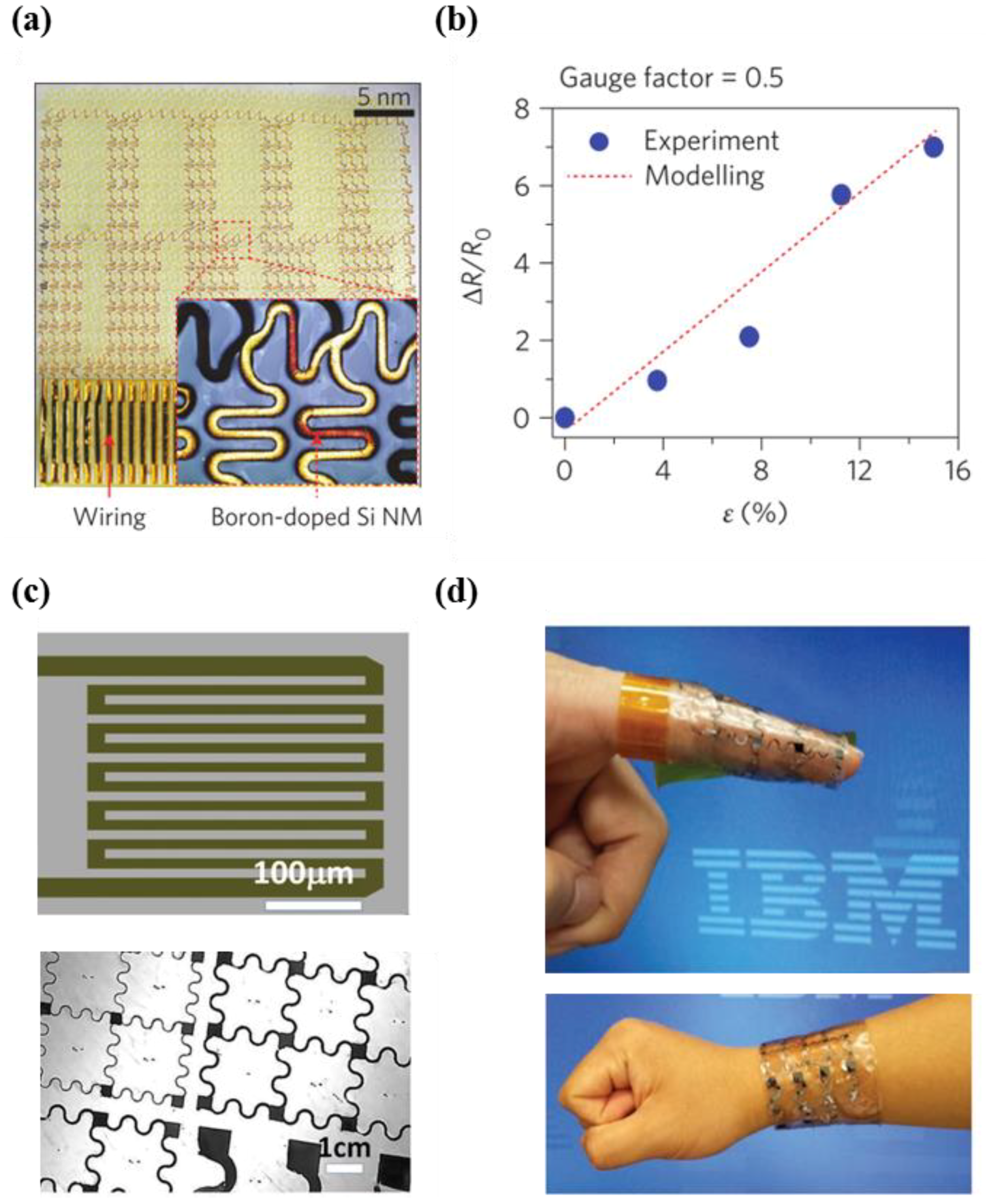
- Kim, J.; Lee, M.; Shim, H.J.; Ghaffari, R.; Cho, H.R.; Son, D.; Jung, Y.H.; Soh, M.; Choi, C.; Jung, S. Stretchable silicon nanoribbon electronics for skin prosthesis. Nat. Commun. 2014, 5, 5747. [Google Scholar] [CrossRef] [PubMed] [Green Version]
- Hua, Q.; Sun, J.; Liu, H.; Bao, R.; Yu, R.; Zhai, J.; Pan, C.; Wang, Z.L. Skin-inspired highly stretchable and conformable matrix networks for multifunctional sensing. Nat. Commun. 2018, 9, 244. [Google Scholar] [CrossRef] [PubMed] [Green Version]
- Zhao, S.; Zhu, R. Electronic skin with multifunction sensors based on thermosensation. Adv. Mater. 2017, 29. [Google Scholar] [CrossRef] [PubMed]
- Zhao, H.; O’Brien, K.; Li, S.; Shepherd, R.F. Optoelectronically innervated soft prosthetic hand via stretchable optical waveguides. Sci. Robot. 2016, 1, eaai7529. [Google Scholar] [CrossRef]
- Zou, Z.; Zhu, C.; Li, Y.; Lei, X.; Zhang, W.; Xiao, J. Rehealable, fully recyclable, and malleable electronic skin enabled by dynamic covalent thermoset nanocomposite. Sci. Adv. 2018, 4, eaaq0508. [Google Scholar] [CrossRef] [PubMed]
- Yao, S.; Zhu, Y. Wearable multifunctional sensors using printed stretchable conductors made of silver nanowires. Nanoscale 2014, 6, 2345–2352. [Google Scholar] [CrossRef] [PubMed]
- Cotton, D.P.; Graz, I.M.; Lacour, S.P. A multifunctional capacitive sensor for stretchable electronic skins. IEEE Sens. J. 2009, 9, 2008–2009. [Google Scholar] [CrossRef]
- Gao, Y.; Ota, H.; Schaler, E.W.; Chen, K.; Zhao, A.; Gao, W.; Fahad, H.M.; Leng, Y.; Zheng, A.; Xiong, F.; et al. Wearable microfluidic diaphragm pressure sensor for health and tactile touch monitoring. Adv. Mater. 2017, 29. [Google Scholar] [CrossRef] [PubMed]
- Someya, T.; Sekitani, T.; Iba, S.; Kato, Y.; Kawaguchi, H.; Sakurai, T. A large-area, flexible pressure sensor matrix with organic field-effect transistors for artificial skin applications. Proc. Nat. Acad. Sci. USA 2004, 101, 9966–9970. [Google Scholar] [CrossRef] [PubMed] [Green Version]
- Jung, S.; Kim, J.H.; Kim, J.; Choi, S.; Lee, J.; Park, I.; Hyeon, T.; Kim, D.H. Reverse-micelle-induced porous pressure-sensitive rubber for wearable human–machine interfaces. Adv. Mater. 2014, 26, 4825–4830. [Google Scholar] [CrossRef] [PubMed]
- Shimojo, M.; Namiki, A.; Ishikawa, M.; Makino, R.; Mabuchi, K. A tactile sensor sheet using pressure conductive rubber with electrical-wires stitched method. IEEE Sens. J. 2004, 4, 589–596. [Google Scholar] [CrossRef]
- Xi, W.; Yeo, J.C.; Yu, L.; Zhang, S.; Lim, C.T. Ultrathin and wearable microtubular epidermal sensor for real-time physiological pulse monitoring. Adv. Mater. Technol. 2017, 2. [Google Scholar] [CrossRef]
- Iwamoto, T.; Shinoda, H. Finger Ring Tactile Interface Based on Propagating Elastic Waves on Human Fingers. In Proceedings of the EuroHaptics Conference, 2007 and Symposium on Haptic Interfaces for Virtual Environment and Teleoperator Systems, Tsukuba, Japan, 22–24 March 2007; pp. 145–150. [Google Scholar]
- Nakatani, M.; Kawasoe, T.; Shiojima, K.; Koketsu, K.; Kinoshita, S.; Wada, J. Wearable Contact Force Sensor System Based on Fingerpad Deformation. In Proceedings of the World Haptics Conference (WHC), Istanbul, Turkey, 21–24 June 2011; pp. 323–328. [Google Scholar]
- Pan, N. Quantification and evaluation of human tactile sense towards fabrics. Int. J. Des. Nat. Ecodyn. 2006, 1, 48–60. [Google Scholar]
- Liu, X.; Yue, Z.; Cai, Z.; Chetwynd, D.G.; Smith, S. Quantifying touch–feel perception: Tribological aspects. Meas. Sci. Technol. 2008, 19, 084007. [Google Scholar] [CrossRef]
- Skedung, L.; Arvidsson, M.; Chung, J.Y.; Stafford, C.M.; Berglund, B.; Rutland, M.W. Feeling small: Exploring the tactile perception limits. Sci. Rep. 2013, 3, 2617. [Google Scholar] [CrossRef] [PubMed]
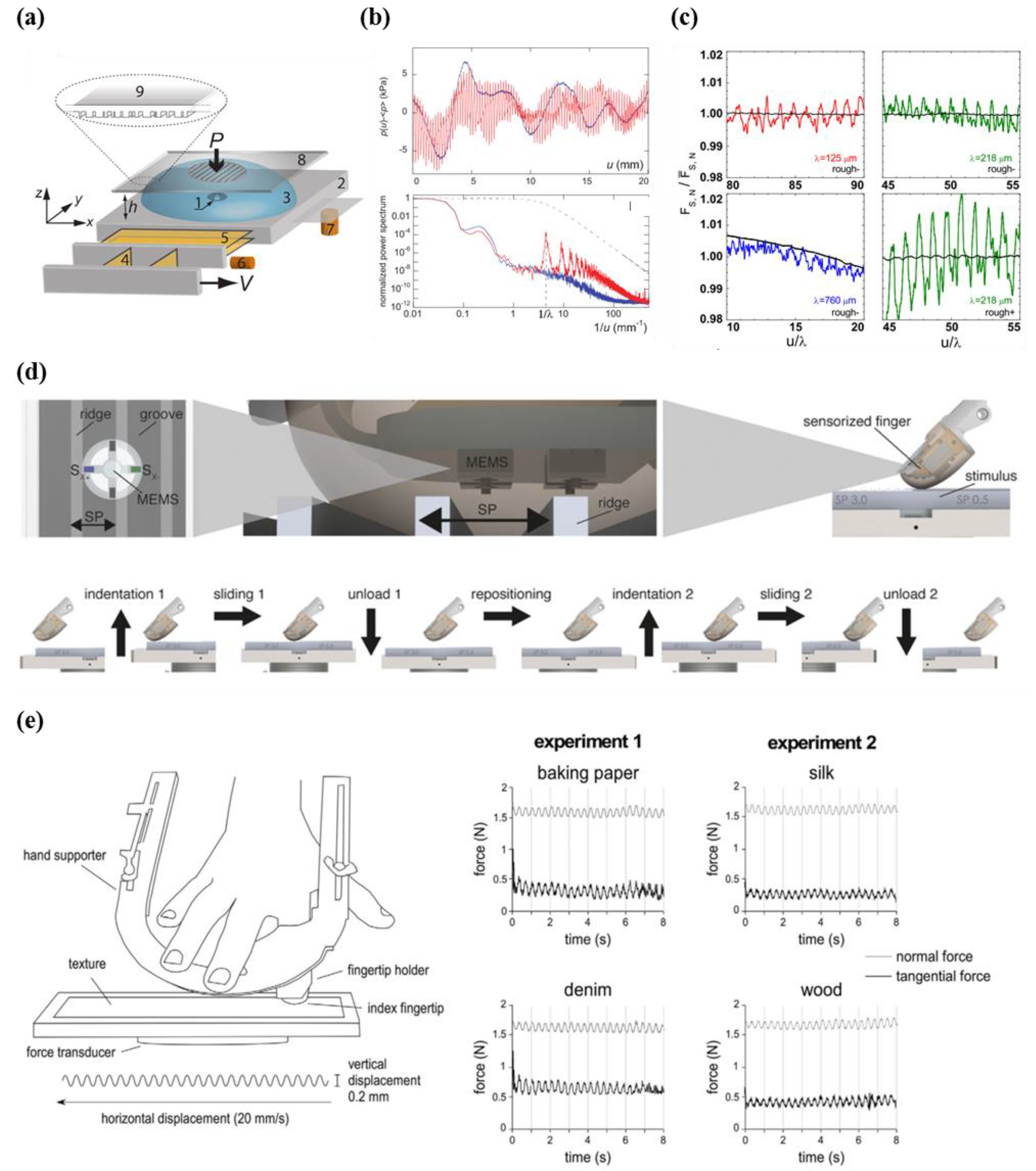
- Scheibert, J.; Leurent, S.; Prevost, A.; Debrégeas, G. The role of fingerprints in the coding of tactile information probed with a biomimetic sensor. Science 2009, 323, 1503–1506. [Google Scholar] [CrossRef] [PubMed]
- Wandersman, E.; Candelier, R.; Debrégeas, G.; Prevost, A. Texture-induced modulations of friction force: The fingerprint effect. Phys. Rev. Lett. 2011, 107, 164301. [Google Scholar] [CrossRef] [PubMed]
- Prevost, A.; Scheibert, J.; Debrégeas, G. Effect of fingerprints orientation on skin vibrations during tactile exploration of textured surfaces. Commun. Integr. Biol. 2009, 2, 422–424. [Google Scholar] [CrossRef] [PubMed]
- Mate, C.M.; Carpick, R.W. Materials science: A sense for touch. Nature 2011, 480, 189–190. [Google Scholar] [CrossRef] [PubMed]
- Moungou, A.; Thonnard, J.-L.; Mouraux, A. Eeg frequency tagging to explore the cortical activity related to the tactile exploration of natural textures. Sci. Rep. 2016, 6, 20738. [Google Scholar] [CrossRef] [PubMed]
- Zahouani, H.; Mezghani, S.; Vargiolu, R.; Hoc, T.; Mansori, M.E. Effect of roughness on vibration of human finger during a friction test. Wear 2013, 301, 343–352. [Google Scholar] [CrossRef]
- Tanaka, Y.; Horita, Y.; Sano, A. Finger-Mounted Skin Vibration Sensor for Active Touch. In Proceedings of the International Conference on Human Haptic Sensing and Touch Enabled Computer Applications, Tampere, Finland, 13–15 June 2012; pp. 169–174. [Google Scholar]
- Fagiani, R.; Massi, F.; Chatelet, E.; Costes, J.P.; Berthier, Y. Contact of a finger on rigid surfaces and textiles: Friction coefficient and induced vibrations. Tribol. Lett. 2012, 48, 145–158. [Google Scholar] [CrossRef] [Green Version]
- Delhaye, B.; Hayward, V.; Lefevre, P.; Thonnard, J.L. Texture-induced vibrations in the forearm during tactile exploration. Front. Behav. Neurosci. 2012, 6, 37. [Google Scholar] [CrossRef] [PubMed]
- Oddo, C.M.; Beccai, L.; Wessberg, J.; Wasling, H.B.; Mattioli, F.; Carrozza, M.C. Roughness encoding in human and biomimetic artificial touch: Spatiotemporal frequency modulation and structural anisotropy of fingerprints. Sensors 2011, 11, 5596–5615. [Google Scholar] [CrossRef] [PubMed] [Green Version]
- Fagiani, R.; Massi, F.; Chatelet, E.; Berthier, Y.; Akay, A. Tactile perception by friction induced vibrations. Tribol. Int. 2011, 44, 1100–1110. [Google Scholar] [CrossRef] [Green Version]
- Martinot, F.; Plenacoste, P.; Chaillou, C. Haptic Sounds and Vibrations of Human Fingerprints. In Proceedings of the International Conference on Sensing Technologies, Palmerston North, NZ, USA, 21–23 November 2005. [Google Scholar]
- Mascaro, S.A.; Asada, H.H. Photoplethysmograph fingernail sensors for measuring finger forces without haptic obstruction. IEEE Trans. Robot. Autom. 2001, 17, 698–708. [Google Scholar] [CrossRef]
- Bensmaïa, S.; Hollins, M. Pacinian representations of fine surface texture. Percept. Psychophys. 2005, 67, 842–854. [Google Scholar] [CrossRef] [PubMed]
- Han, H.-Y.; Shimada, A.; Kawamura, S. Analysis of Friction on Human Fingers and Design of Artificial Fingers. In Proceedings of the IEEE International Conference on Robotics and Automation, Minneapolis, MN, USA, 22–28 April 1996; pp. 3061–3066. [Google Scholar]
- Puangmali, P.; Althoefer, K.; Seneviratne, L.D.; Murphy, D.; Dasgupta, P. State-of-the-art in force and tactile sensing for minimally invasive surgery. IEEE Sens. J. 2008, 8, 371–381. [Google Scholar] [CrossRef]
- Enayati, N.; De Momi, E.; Ferrigno, G. Haptics in robot-assisted surgery: Challenges and benefits. IEEE Rev. Biomed. Eng. 2016, 9, 49–65. [Google Scholar] [CrossRef] [PubMed]
- Eltaib, M.; Hewit, J. Tactile sensing technology for minimal access surgery––A review. Mechatronics 2003, 13, 1163–1177. [Google Scholar] [CrossRef]
- Hu, Y.; Katragadda, R.B.; Tu, H.; Zheng, Q.; Li, Y.; Xu, Y. Bioinspired 3-D tactile sensor for minimally invasive surgery. J. Microelectromech. Syst. 2010, 19, 1400–1408. [Google Scholar] [CrossRef]
- Kim, U.; Lee, D.-H.; Yoon, W.J.; Hannaford, B.; Choi, H.R. Force sensor integrated surgical forceps for minimally invasive robotic surgery. IEEE Trans. Robot. 2015, 31, 1214–1224. [Google Scholar] [CrossRef]
- Ly, H.H.; Tanaka, Y.; Fukuda, T.; Sano, A. Grasper having tactile sensing function using acoustic reflection for laparoscopic surgery. Int. J. Comput. Assist. Radiol. Surg. 2017, 12, 1333–1343. [Google Scholar] [CrossRef] [PubMed]


| Meissner Corpuscle | Pacinian Corpuscle | Merkel Cell | Ruffini Endings | |
|---|---|---|---|---|
| Classification | RA-I | RA-II | SA-I | SA-II |
| Adaptation rate | Fast | Fast | Slow | Slow |
| Location | Shallow | Deep | Shallow | Deep |
| Stimuli frequency (Hz) | 10–200 | 70–1000 | 0.4–100 | 0.4–100 |
| Density (units/cm2) | 140 | 20 | 70 | 10 |
| Spatial resolution (mm) | 3–4 | 10+ | 0.5 | 7+ |
| Functions | Object slip, Light touch, texture | High-frequency Vibrations | Static forces with high resolution | Tension deep in the skin and fascia |
| Receptive field (RF) | Small and sharp, 3–5 mm | Very large and diffuse, >20 mm | Small and sharp, 2–3 mm | Large and diffuse, 10–15 mm |
© 2018 by the authors. Licensee MDPI, Basel, Switzerland. This article is an open access article distributed under the terms and conditions of the Creative Commons Attribution (CC BY) license (http://creativecommons.org/licenses/by/4.0/).
Share and Cite
Park, M.; Bok, B.-G.; Ahn, J.-H.; Kim, M.-S. Recent Advances in Tactile Sensing Technology. Micromachines 2018, 9, 321. https://doi.org/10.3390/mi9070321
Park M, Bok B-G, Ahn J-H, Kim M-S. Recent Advances in Tactile Sensing Technology. Micromachines. 2018; 9(7):321. https://doi.org/10.3390/mi9070321
Chicago/Turabian StylePark, Minhoon, Bo-Gyu Bok, Jong-Hyun Ahn, and Min-Seok Kim. 2018. "Recent Advances in Tactile Sensing Technology" Micromachines 9, no. 7: 321. https://doi.org/10.3390/mi9070321
APA StylePark, M., Bok, B.-G., Ahn, J.-H., & Kim, M.-S. (2018). Recent Advances in Tactile Sensing Technology. Micromachines, 9(7), 321. https://doi.org/10.3390/mi9070321