Sol-Gel Template Synthesis and Characterization of Lu2O3:Eu3+ Nanowire Arrays

Abstract
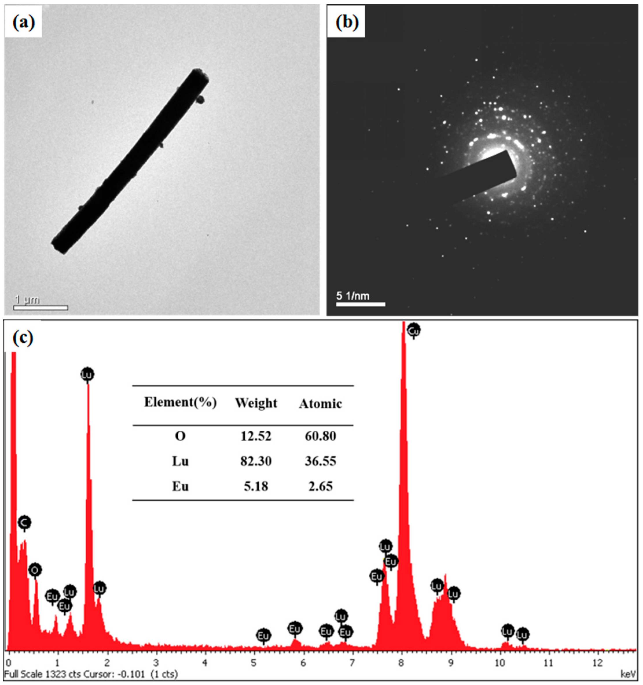
:
1. Introduction
2. Materials and Methods
2.1. Material
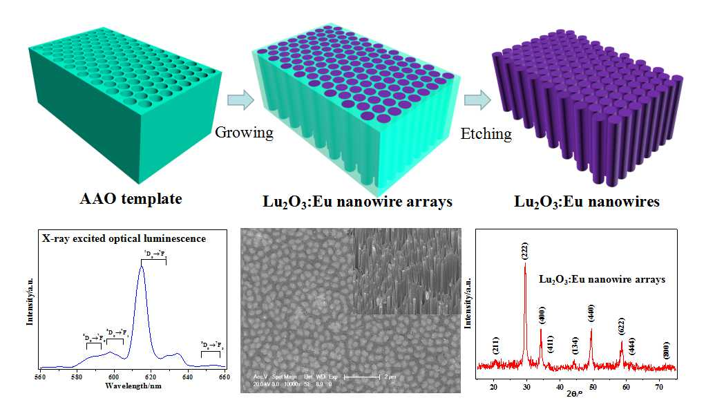
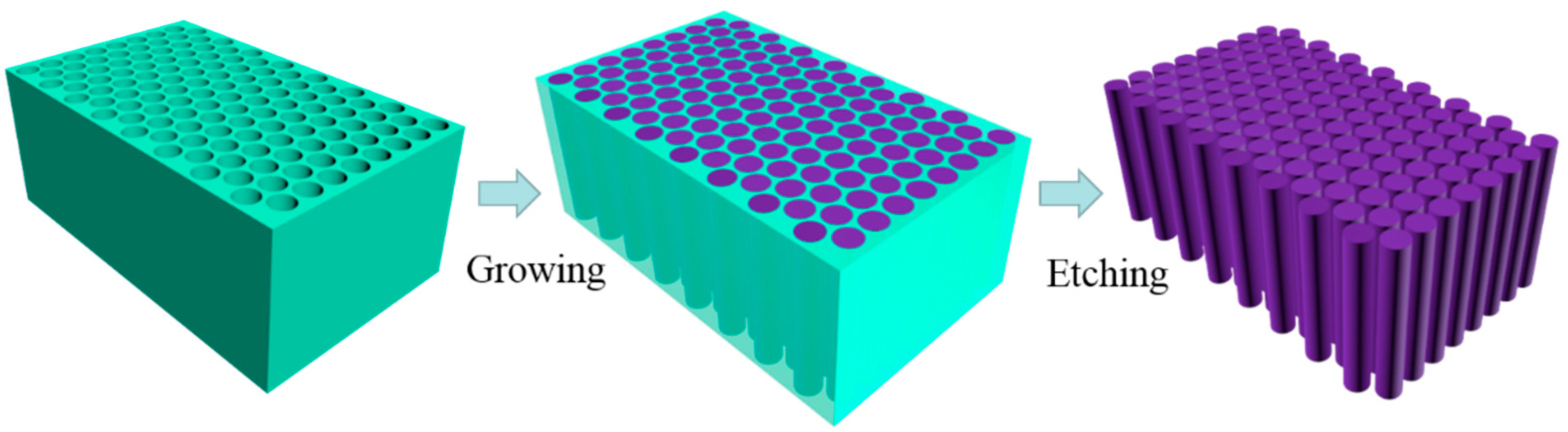
2.2. Preparation of Lu2O3:Eu3+ Nanowire Arrays
2.3. Characterization of Lu2O3:Eu3+ Nanowire Arrays
3. Results and Discussion
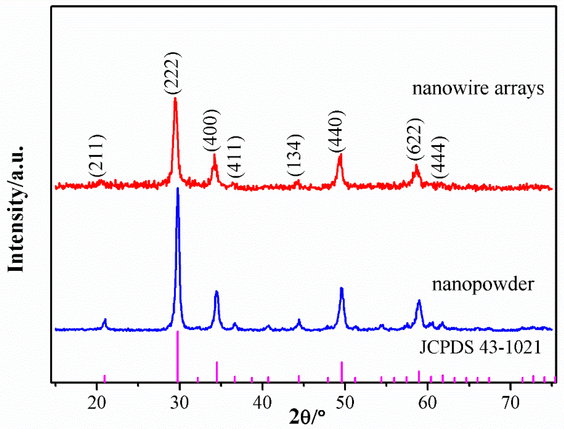
3.1. Structure and Surface Morphology of Lu2O3:Eu3+ Nanowire Arrays
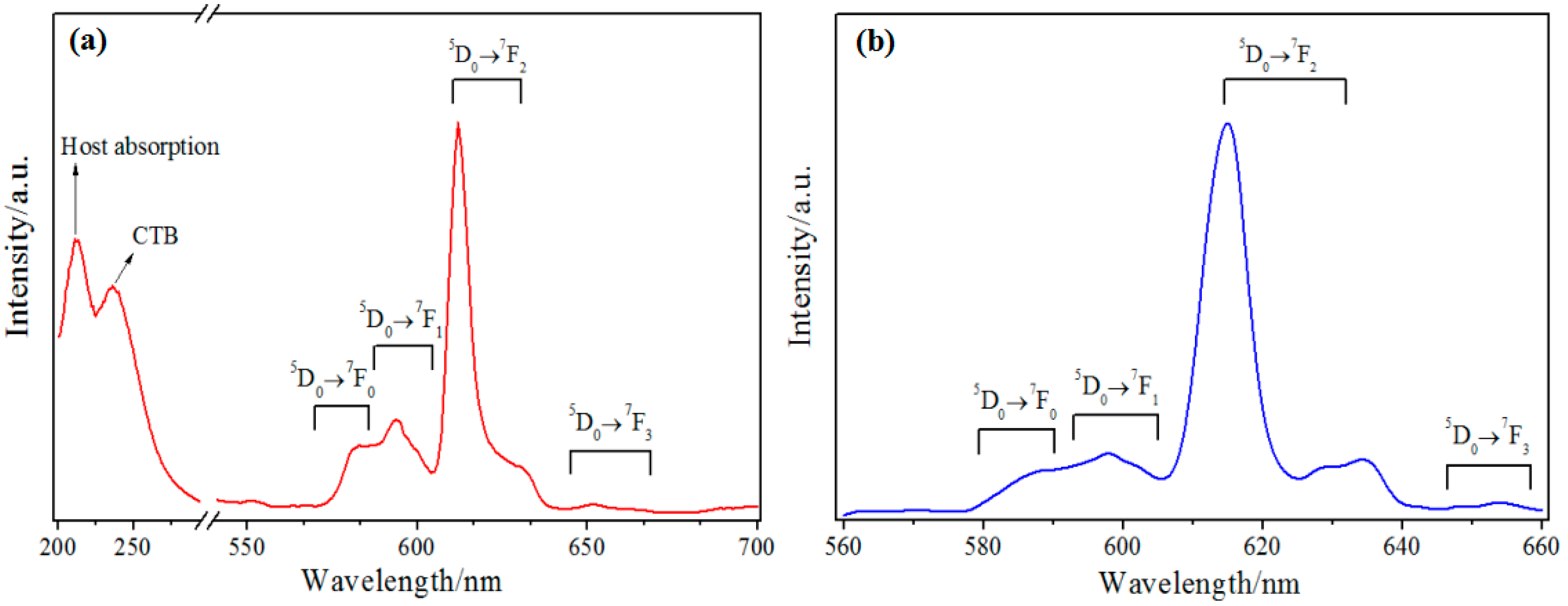
3.2. Luminescence Properties of the Lu2O3:Eu3+ Nanowire Arrays
4. Conclusions
Author Contributions
Funding
Conflicts of Interest
References
- Wallentin, J.; Anttu, N.; Asoli, D.; Huffman, M.; Aberg, I.; Magnusson, M.H.; Siefer, G.; Kailuweit, P.F.; Dimroth, F.; Witzigmann, B.; et al. InP nanowire array solar cells achieving 13.8% efficiency by exceeding the ray optics limit. Science 2013, 339, 1057–1060. [Google Scholar] [CrossRef] [PubMed]
- Wu, Y.; Yan, H.; Yang, P. Semiconductor nanowire array: Potential substrates for photocatalysis and photovoltaics. Top. Catal. 2002, 19, 197–202. [Google Scholar] [CrossRef]
- Cao, B.; Chen, J.; Tang, C.; Zhou, W. Growth of monoclinic WO3 nanowire array for highly sensitive NO2 detection. Mater. Chem. 2009, 19, 2323–2327. [Google Scholar] [CrossRef]
- Xia, Y.; Yang, P.; Sun, Y.; Wu, Y.; Mayers, B.; Gates, B.; Yin, Y.; Kim, F.; Yan, H. One-dimensional nanostructures: Synthesis, characterization, and applications. Adv. Mater. 2003, 15, 353–359. [Google Scholar] [CrossRef]
- Barth, S.; Hernandez-Ramirez, F.; Holmes, J.D. Synthesis and applications of one-dimensional semiconductors. Prog. Mater. Sci. 2010, 55, 563–627. [Google Scholar] [CrossRef]
- Peng, K.; Wang, X.; Lee, S. Silicon nanowire array photoelectrochemical solar cells. Appl. Phys. Lett. 2008, 92, 163103. [Google Scholar] [CrossRef]
- Bai, Y.; Sun, Y.; Sun, C. Pt–Pb nanowire array electrode for enzyme-free glucose detection. Biosens. Bioelectron. 2008, 24, 579–585. [Google Scholar] [CrossRef] [PubMed]
- Li, Y.; Huang, Y.; Yan, L.; Qi, S.; Miao, L.; Wang, Y.; Wang, Q. Synthesis and magnetic properties of ordered barium ferrite nanowire arrays in AAO template. Appl. Surf. Sci. 2011, 257, 8974–8980. [Google Scholar] [CrossRef]
- Lee, W.; Park, S.J. Porous anodic aluminum oxide: Anodization and templated synthesis of functional nanostructures. Chem. Rev. 2014, 114, 7487–7556. [Google Scholar] [CrossRef] [PubMed]
- Md Jani, A.M.; Losic, D.; Voelcker, N.H. Nanoporous anodic aluminium oxide: Advances in surface engineering and emerging applications. Prog. Mater. Sci. 2013, 58, 636–704. [Google Scholar] [CrossRef]
- Chen, C.; Chen, S.; Chen, C.; Lin, J. Using positive pressure to produce a sub-micron single-crystal column of cesium iodide (CsI) for scintillator formation. Mater. Lett. 2015, 148, 138–141. [Google Scholar] [CrossRef]
- Wang, F.; Wang, J.; Zhong, X.; Li, B.; Zhou, Y. Synthesis and characterization of Bi3.15Nd0.85Ti3O12 nanotube arrays. J. Cryst. Growth 2009, 311, 4495–4498. [Google Scholar] [CrossRef]
- Shankar, K.S.; Raychaudhuri, A.K. Fabrication of nanowires of multicomponent oxides: Review of recent advances. Mater. Sci. Eng. C 2005, 25, 738–751. [Google Scholar] [CrossRef]
- Seferis, I.; Michail, C.; Valais, I.; Zeler, J.; Liaparinos, P.; Fountos, G.; Kalyvas, N.; David, S.; Stromatia, F.; Zych, E.; et al. Light emission efficiency and imaging performance of Lu2O3:Eu nanophosphor under X-ray radiography conditions: Comparison with Gd2O2S:Eu. J. Lumin. 2014, 151, 229–234. [Google Scholar] [CrossRef]
- Xie, J.; Deng, L.; Shi, Y.; Xie, J.; Qiu, H.; Song, G. The influence of Pr3+ co-doping on the luminescent properties of Lu2O3:5mol% Eu films. J. Lumin. 2011, 131, 970–974. [Google Scholar]
- Liu, X.; Li, H.; Xie, R.; Hirosaki, N.; Xu, X.; Huang, L. Synthesis, characterization, and luminescent properties of Lu2O3:Eu phosphors. J. Lumin. 2007, 127, 469–473. [Google Scholar] [CrossRef]
- Lempicki, A.; Brecher, C.; Szupryczynski, P.; Lingertat, H.; Nagarkar, V.V.; Tipnis, S.V.; Miller, S.R. A new lutetia-based ceramic scintillator for X-ray imaging. Nucl. Instrum. Methods Phys. Res. Sect. A 2002, 488, 579–590. [Google Scholar] [CrossRef]
- Topping, S.G.; Sarin, V.K. CVD Lu2O3:Eu coatings for advanced scintillators. Int. J. Refract. Met. Hard Mater. 2009, 27, 498–501. [Google Scholar] [CrossRef] [PubMed]
- Chen, C.; Chang, S.; Luo, Z. Anodic-aluminum-oxide template assisted fabrication of cesium iodide (CsI) scintillator nanowires. Mater. Lett. 2013, 112, 190–193. [Google Scholar] [CrossRef]
- Zhang, Z.; Gu, M.; Hu, Y.; Liu, X.; Huang, S.; Liu, B.; Ni, C. Template synthesis and luminescence of ordered Lu3Al5O12:Ce3+ nanowire arrays. Mater. Lett. 2016, 166, 158–162. [Google Scholar] [CrossRef]
- Bezkrovnyi, O.S.; Babayevskaya, N.V.; Mateychenko, P.V.; Vovk, O.M.; Doroshenko, A.G.; Sofronov, D.S. Structure and morphological stability of (Lu1−xEux)2O3 thin film. Cryst. Res. Technol. 2014, 49, 85–91. [Google Scholar] [CrossRef]


© 2018 by the authors. Licensee MDPI, Basel, Switzerland. This article is an open access article distributed under the terms and conditions of the Creative Commons Attribution (CC BY) license (http://creativecommons.org/licenses/by/4.0/).
Share and Cite
Hu, Y.; Gu, M.; Liu, X.; Zhang, J.; Huang, S.; Liu, B. Sol-Gel Template Synthesis and Characterization of Lu2O3:Eu3+ Nanowire Arrays. Micromachines 2018, 9, 601. https://doi.org/10.3390/mi9110601
Hu Y, Gu M, Liu X, Zhang J, Huang S, Liu B. Sol-Gel Template Synthesis and Characterization of Lu2O3:Eu3+ Nanowire Arrays. Micromachines. 2018; 9(11):601. https://doi.org/10.3390/mi9110601
Chicago/Turabian StyleHu, Yahua, Mu Gu, Xiaolin Liu, Juannan Zhang, Shiming Huang, and Bo Liu. 2018. "Sol-Gel Template Synthesis and Characterization of Lu2O3:Eu3+ Nanowire Arrays" Micromachines 9, no. 11: 601. https://doi.org/10.3390/mi9110601
APA StyleHu, Y., Gu, M., Liu, X., Zhang, J., Huang, S., & Liu, B. (2018). Sol-Gel Template Synthesis and Characterization of Lu2O3:Eu3+ Nanowire Arrays. Micromachines, 9(11), 601. https://doi.org/10.3390/mi9110601