Introduction of a Chemical-Free Metal PDMS Thermal Bonding for Fabrication of Flexible Electrode by Metal Transfer onto PDMS


Abstract
:1. Introduction
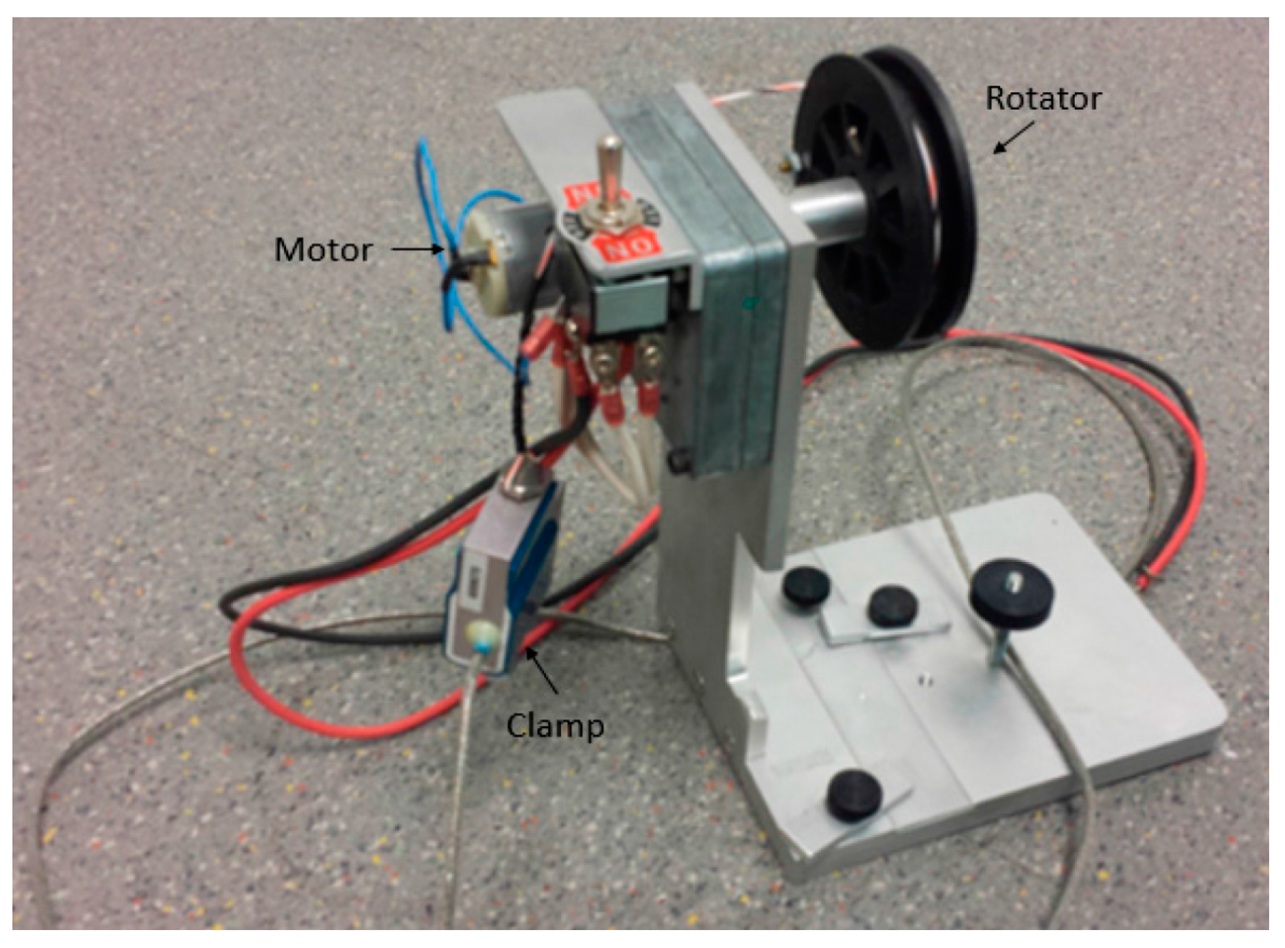
2. Method/Experiment
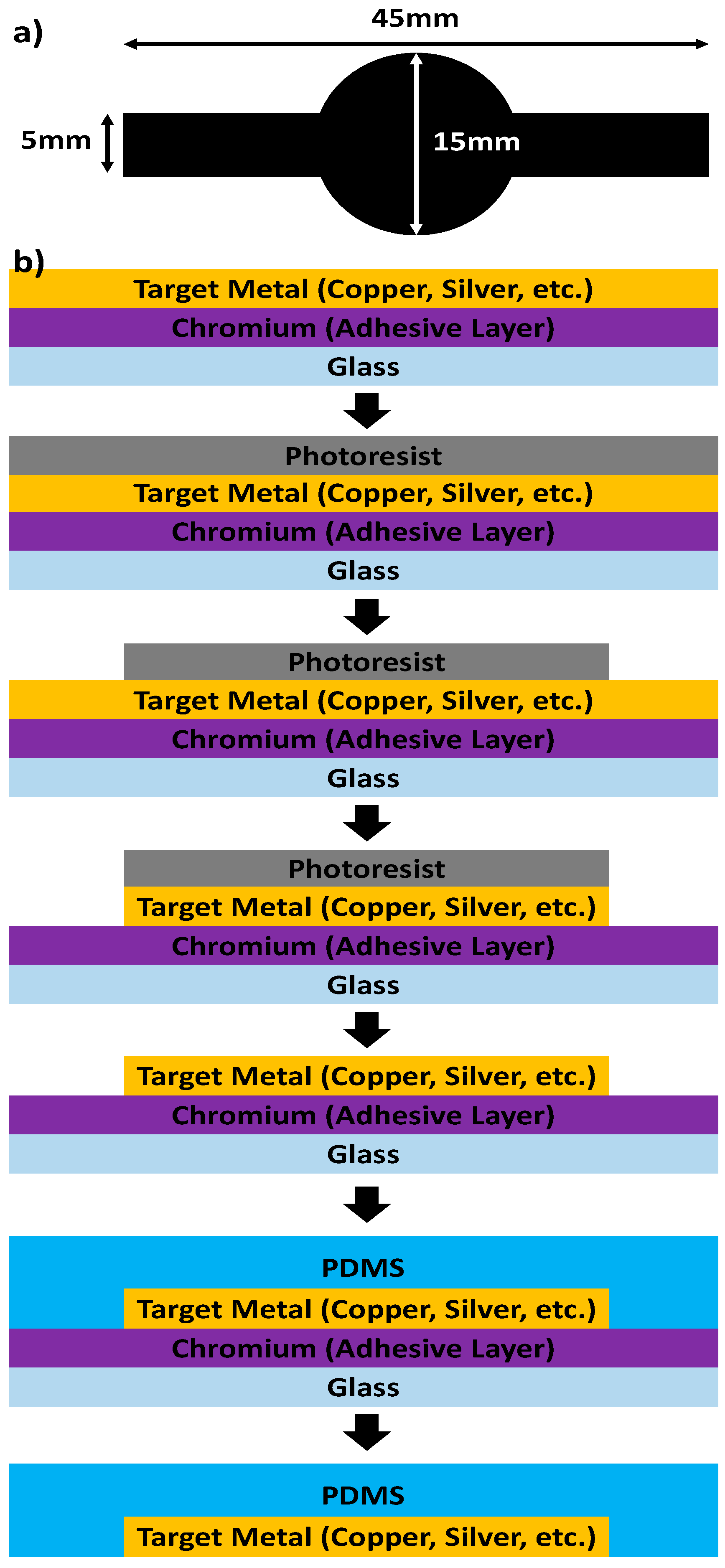
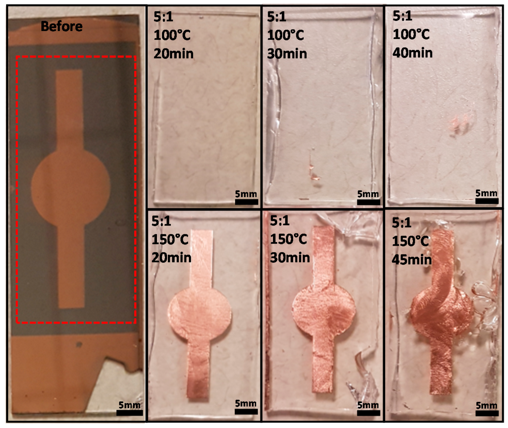
2.1. Demonstration of Metal Transfer and the Study of Various PDMS Curing Conditions
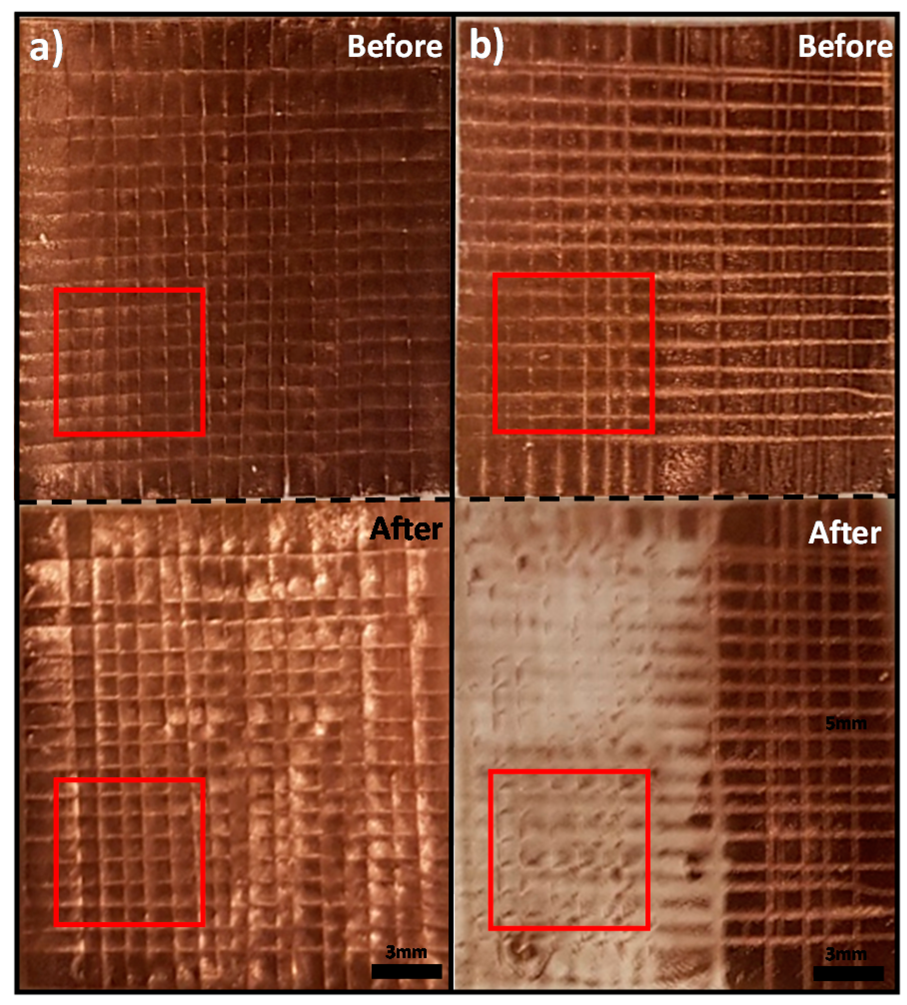
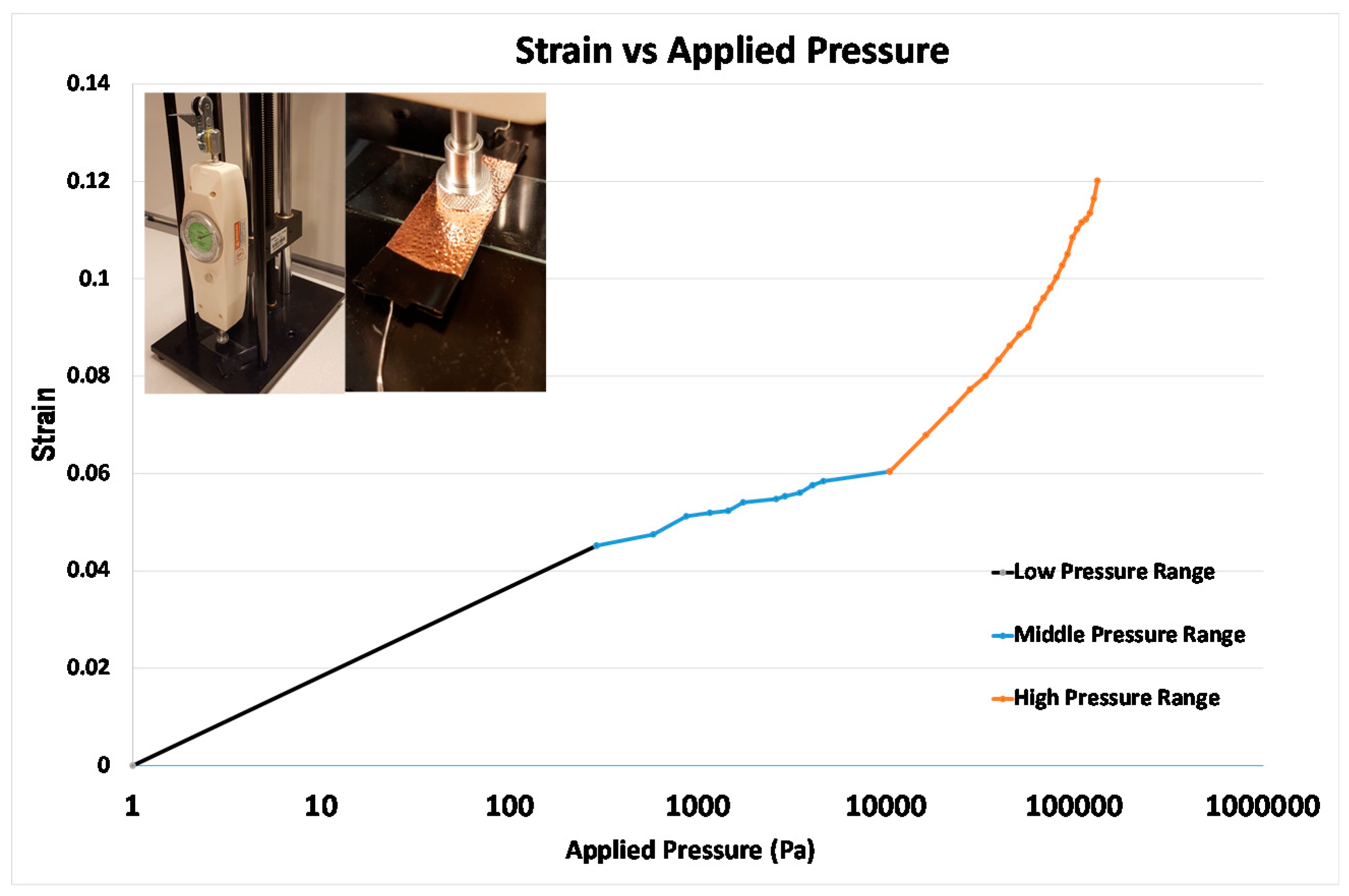
2.2. Bonding Strength Test
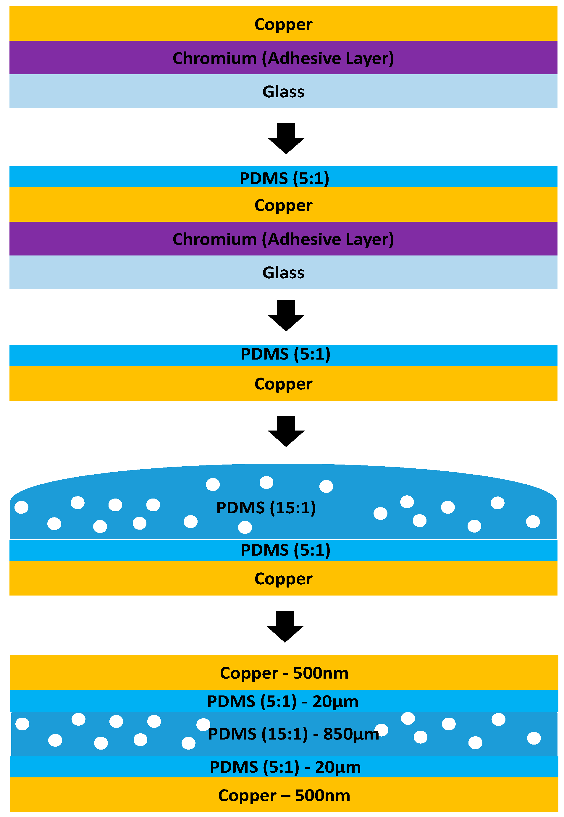
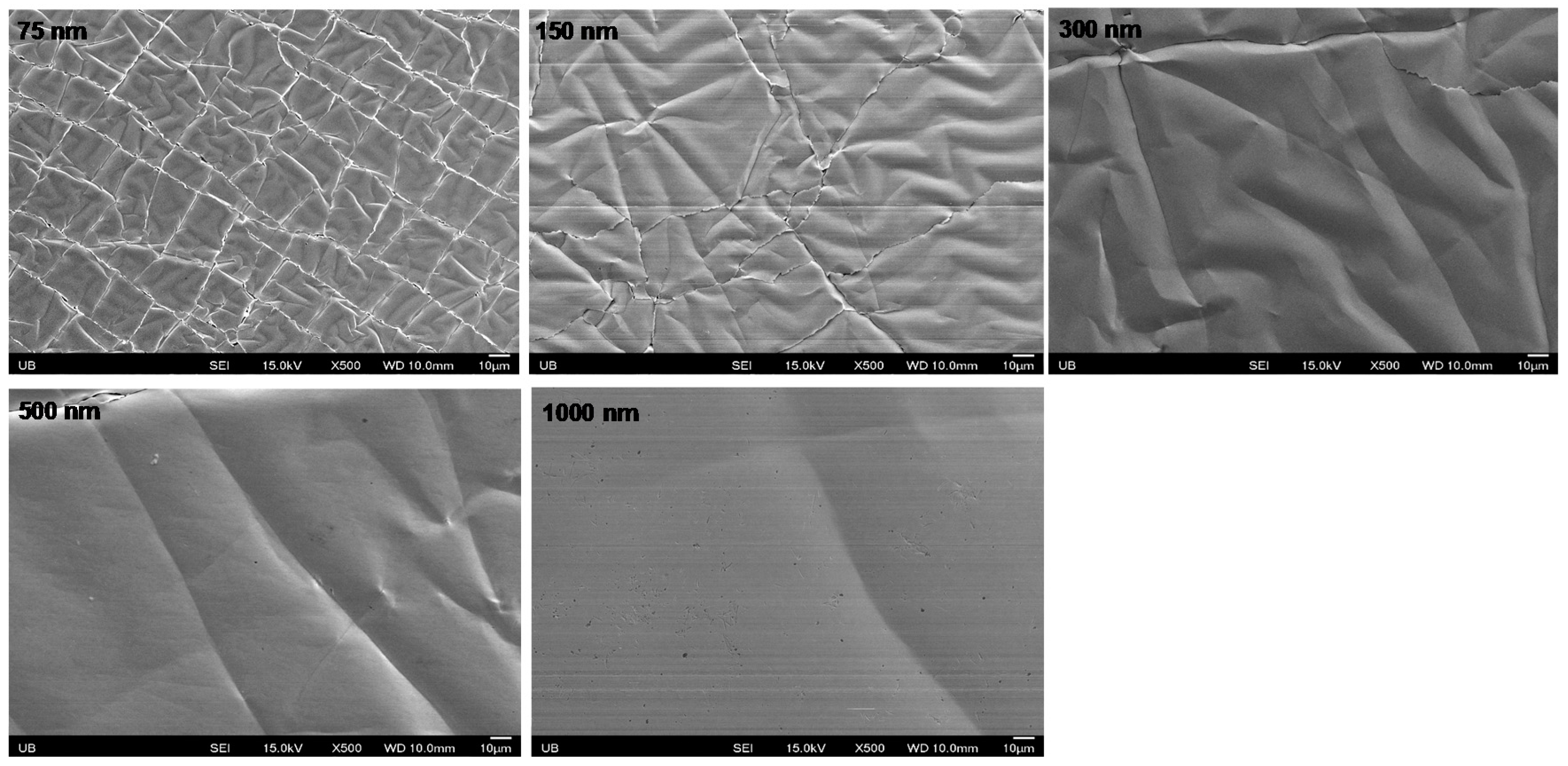
2.3. Study of Optimum Electrode Thickness
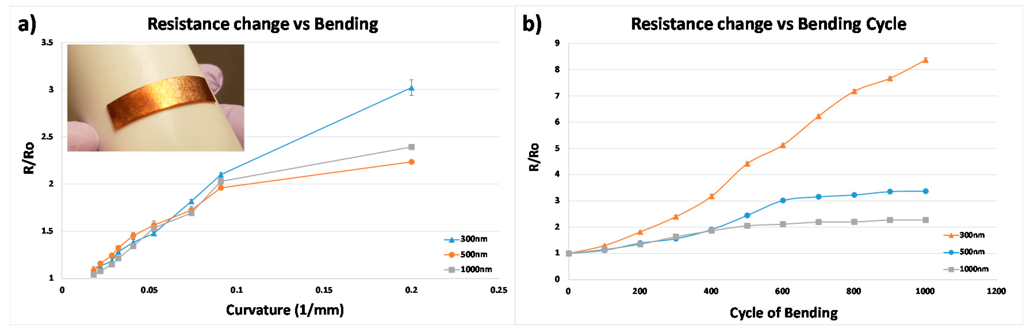
2.4. Study of the Resistance Change Flexible Electrode
2.5. Study of Pressure Sensor
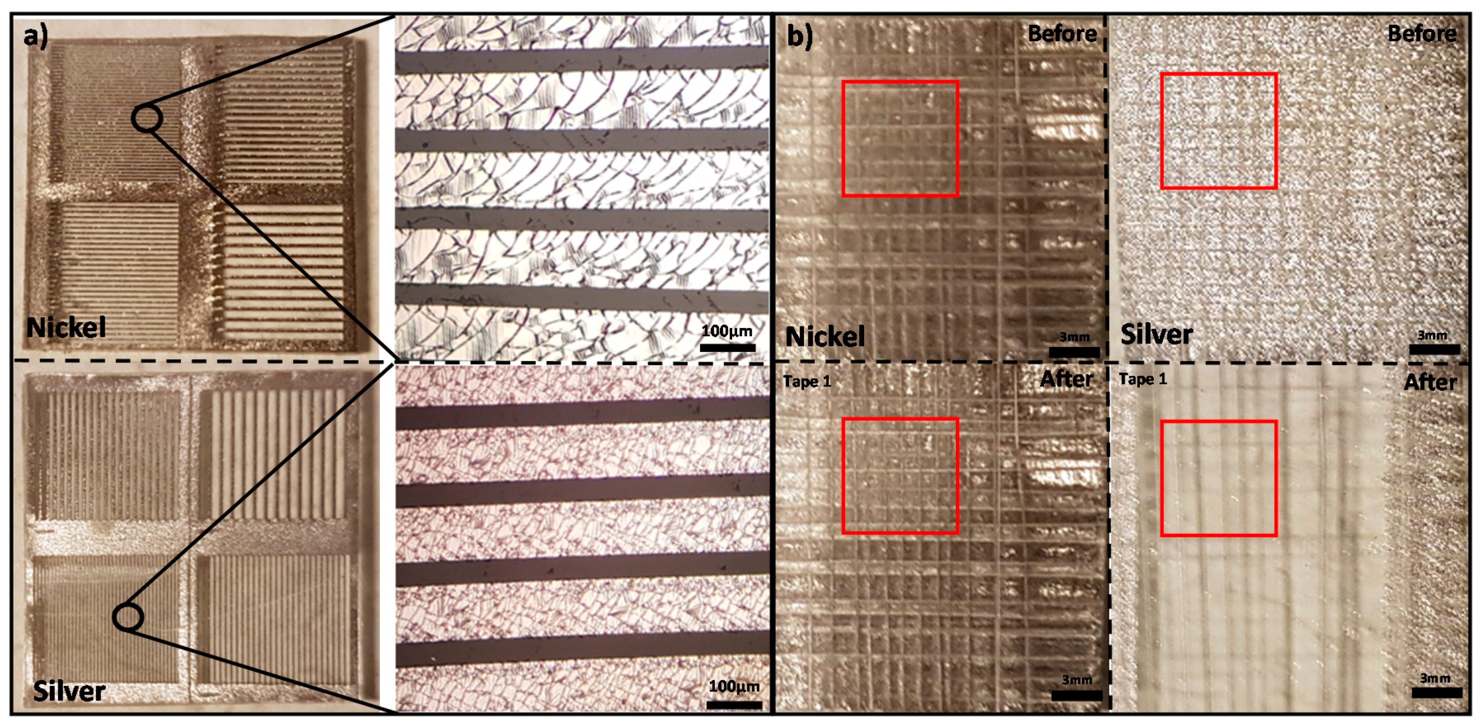
2.6. Study of Different Metal Transfers
3. Results and Discussion
3.1. Results of Metal Transfer Condition
3.2. Bonding Strength Test Results
3.3. Result of Optimum Electrode Thickness
3.4. Result of the Resistance Change Flexible Electrode
3.5. The Result of Pressure Sensors
3.6. The Result of Different Metal Transfers
4. Conclusions
Acknowledgments
Author Contributions
Conflicts of Interest
References
- Zhou, J.; Ellis, A.V.; Voelcker, N.H. Recent Developments in PDMS surface modification for microfluidic devices. Electrophoresis 2010, 31, 2–16. [Google Scholar] [CrossRef] [PubMed]
- Patel, J.N.; Kaminska, B.; Gray, B.L.; Gates, B.D. A sacrificial SU-8 mask for direct metallization on PDMS. J. Micromech. Microeng. 2009, 19, 115014. [Google Scholar] [CrossRef]
- Lim, K.S.; Chang, W.-J.; Koo, Y.-M.; Bashir, R. Reliable fabrication method of transferable micron scale metal pattern for poly(dimethylsiloxane) metallization. Lab Chip 2006, 6, 578–580. [Google Scholar] [CrossRef] [PubMed]
- Bodas, D.; Khan-Malek, C. Hydrophilization and hydrophobic recovery of PDMS by oxygen plasma and chemical treatment-An SEM investigation. Sens. Actuators B 2007, 123, 368–373. [Google Scholar] [CrossRef]
- Byun, I.; Coleman, A.W.; Kim, B. Transfer of thin Au films to polydimethylsiloxane (PDMS) with reliable bonding using (3-mercaptopropyl)trimethoxysilane (MPTMS) as a molecular adhesive. J. Micromech. Microeng. 2013, 23, 085016. [Google Scholar] [CrossRef]
- Byun, I.; Ueno, R.; Kim, B. Micro-heaters embedded in PDMS fabricated using dry peel-off process. Microelectr. Eng. 2014, 121, 1–4. [Google Scholar] [CrossRef]
- Couty, M.; Woytasik, M.; Ginefri, J.-C.; Rubin, A.; Martincic, E.; Poirier-Quinot, M.; Darrasse, L.; Boumezbeur, F.; Lethimonnier, F.; Tatoulian, M.; et al. Fabrication and Packaging of Flexible Polymeric Microantennae for in Vivo Magnetic Resonance Imaging. Polymers 2012, 4, 656–673. [Google Scholar] [CrossRef]
- Couty, M.; Nazer, S.; Jelita, C.; Martincic, E.; Woytasik, M.; Ginefri, J.-C.; Darrasse, L.; Tatoulian, M.; Dufour-Gergam, E. Fabrication of metallic patterns on polydimethylsiloxane using transfer technology: Application to MRI microcoils. Micro Nano Lett. 2012, 7, 519–522. [Google Scholar] [CrossRef]
- Couty, M.; Nazeer, S.; Jelita, C.; Martincic, E.; Woytasik, M.; Ginefri, J.C.; Darrasse, L.; Tatoulian, M.; Dufour-Gergam, E. Ultra-flexible micro-antennas on PDMS substrate for MRI applications. In Proceedings of the 2012 Symposium on Design, Test, Integration and Packaging of MEMS/MOEMS (DTIP), Cannes, France, 25–27 April 2012. [Google Scholar]
- Zhu, M.; Lee, C. Facile metal transfer method for fabricating unconventional metamaterial devices. Opt. Mater. Exp. 2015, 5, 733–741. [Google Scholar] [CrossRef]
- Khan, Y.; Pavinatto, F.J.; Lin, M.C.; Liao, A.; Swisher, S.L.; Mann, K.; Subramanian, V.; Maharbiz, M.M.; Arias, A.C. Inkjet-Printed Flexible Gold Electrode Arrays for Bioelectronic Interfaces. Adv. Funct. Mater. 2016, 26, 1004–1013. [Google Scholar] [CrossRef]
- Kung, Y.-C.; Huang, K.-W.; Fan, Y.-J.; Chiou, P.-Y. Fabrication of 3D high aspect ratio PDMS microfluidic networks with a hybrid stamp. Lab Chip 2015, 15, 1861. [Google Scholar] [CrossRef] [PubMed]
- Lee, H.; Koh, D.; Xu, L.; Row, S.; Andreadis, S.T.; Oh, K.W. A Simple Method for Fabrication of Microstructures Using a PDMS Stamp. Micromachines 2016, 7, 173. [Google Scholar] [CrossRef]
- American Society for Testing and Materials (ASTM). D-3359-2 Cross-Cut Tape Test for Adhesion; American Society for Testing and Materials (ASTM): West Conshohocken, PA, USA, 2006. [Google Scholar]
- Lu, N.; Suo, Z.; Vlassak, J.J. The effect of film thickness on the failure strain of polymer-supported metal films. Acta Mater. 2010, 58, 1679–1687. [Google Scholar] [CrossRef]
- Lee, B.-Y.; Kim, J.; Kim, H.; Kim, C.; Lee, S.-D. Low-cost flexible pressure sensor based on dielectric elastomer film with micro-pores. Sens. Actuators A 2016, 240, 103–109. [Google Scholar] [CrossRef]
- Lai, C.-C.; Chiu, H.-K.; Lin, Y.-P.; Kuan, Y.-C.; Sun, O. Quantitative Adhesion Analysis of Sputtered Copper Films on Glass Substrate by Microindentation Measurement; SID Symposium Digest of Technical Papers; Blackwell Publishing Ltd.: Hoboken, NJ, USA, 2006; Volume 37. [Google Scholar]
- Xiang, Y.; Vlassak, J.J. Bauschinger and size effects in thin-film plasticity. Acta Mater. 2006, 54, 5449. [Google Scholar] [CrossRef]
- Srolovitz, D.J.; Battaile, C.C.; Li, X.; Butler, J.E. Simulation of faceted film growth in two-dimensions: Microstructure, morphology and texture. Acta Mater. 1999, 47, 2269–2281. [Google Scholar]
- Dammers, A.J.; Radelaar, S. CP90 Europhysics Conference on Computational Physics; Tenner, A., Ed.; World Scientific®: Singapore, 1991; p. 310. [Google Scholar]
- Dammers, A.J.; Radelaar, S. Two-Dimensional Computer Modelling of Polycrystalline Film Growth. Textures Microstruct. 1991, 757, 14. [Google Scholar] [CrossRef]
- Dammers, A.J.; Radelaar, S. A Grain Growth Model for Evolution of Polycrystalline Surfaces. Mater. Sci. Forum 1992, 345, 94–96. [Google Scholar] [CrossRef]
- Zhang, X.; Sing, X.-H.; Zhang, D.-L. Thickness dependence of grain size and surface roughness for dc magnetron sputtered Au films. Chin. Phys. B 2010, 19, 086802. [Google Scholar]
- Meyers, M.A.; Mishra, A.; Benson, D.J. Mechanical properties of nanocrystalline materials. Prog. Mater. Sci. 2006, 51, 427–556. [Google Scholar] [CrossRef]
- Bowden, N.; Britten, S.; Evans, A.G.; Hutchinson, J.W.; Whitesides, G.M. Spontaneous formation of ordered structures in thin films of metals supported on an elastomeric polymer. Nature 1998, 393, 146–148. [Google Scholar]
- Bowden, N.; Huck, W.T.S.; Paul, K.E.; Whitesidesa, G.M. The controlled formation of ordered, sinusoidal structures by plasma oxidation of an elastomeric polymer. Appl. Phys. Lett. 1999, 75, 2557–2559. [Google Scholar] [CrossRef]
- Lee, H.; Kim, I.; Kimb, M.; Lee, H. Moving beyond flexible to stretchable conductive electrodes using metal nanowires and graphenes. Nanoscale 2016, 8, 1789–1822. [Google Scholar] [CrossRef] [PubMed]
- Khaund, A.; Nicholson, P. Fracture of a brittle composite: influence of elastic mismatch and interfacial bonding. J. Mater. Sci. 1980, 15, 177–187. [Google Scholar] [CrossRef]
- Schmid, H.; Wolf, H.; Allenspach, R.; Riel, H.; Karg, S.; Michel, B.; Delamarche, E. Preparation of Metallic Films on Elastomeric Stamps and Their Application for Contact Processing and Contact Printing. Adv. Funct. Mater. 2003, 13, 145–153. [Google Scholar] [CrossRef]
- Kim, D.-H.; Liu, Z.; Kim, Y.-S.; Wu, J.; Song, J.; Kim, H.-S.; Huang, Y.; Hwang, K.-C.; Zhang, Y.; Rogers, J.A. Optimized Structural Designs for Stretchable Silicon Integrated Circuits. Small 2009, 5, 2841–2847. [Google Scholar] [CrossRef] [PubMed]
- Kim, R.-H.; Kim, D.-H.; Xiao, J.; Kim, B.H.; Park, S.-I.; Panilaitis, B.; Ghaffari, R.; Yao, J.; Li, M.; Liu, Z.; et al. Waterproof AlInGaP Optoelectronics on Stretchable Substrates with Applications in Biomedicine and Robotics. Nat. Mater. 2010, 9, 929–937. [Google Scholar] [CrossRef] [PubMed]
- Yu, C.; Duan, Z.; Yuan, P.; Li, Y.; Su, Y.; Zhang, X.; Pan, Y.; Dai, L.L.; Nuzzo, R.G.; Huang, Y.; et al. Electronically Programmable, Reversible Shape Change in Two- and Three-Dimensional Hydrogel Structures. Adv. Mater. 2013, 25, 1541–1546. [Google Scholar] [CrossRef] [PubMed]
- Zhang, Y.; Xu, S.; Fu, H.; Lee, J.; Su, J.; Hwang, K.-C.; Rogers, J.A.; Huang, Y. Buckling in serpentine microstructures and applications in elastomer-supported ultra-stretchable electronics with high areal coverage. Soft Matter 2013, 9, 8062–8070. [Google Scholar] [CrossRef] [PubMed]
- Wang, Z.; Volinsky, A.A.; Gallant, N.D. Crosslinking Effect on Polydimethylsiloxane Elastic Modulus Measured by Custom-Built Compression Instrument. J. Appl. Polym. Sci. 2014. [Google Scholar] [CrossRef]
- Zhu, T.; Cheng, R.; Lee, S.A.; Rajaraman, E.; Eiteman, M.A.; Querec, T.D.; Unger, E.R.; Mao, L. Continuous-flow Ferrohydrodynamic Sorting of Particles and Cells in Microfluidic Devices. Microfluid. Nanofluidics 2012, 13, 645–654. [Google Scholar] [CrossRef] [PubMed]
- Chon, H.; Lim, C.; Ha, S.-M.; Ahn, Y.; Lee, E.K.; Chang, S.I.; Seong, G.H.; Choo, J. On-Chip Immunoassay Using Surface-Enhanced Raman Scattering of Hollow Gold Nanospheres. Anal. Chem. 2010, 82, 5290–5295. [Google Scholar] [CrossRef] [PubMed]


| Trial | Temperature (°C) | Mixing Ratio | Baking Time (min) | Transfer Result |
|---|---|---|---|---|
| 1 | 100 | 20:1 | 20 | X |
| 2 | 100 | 10:1 | 20 | X |
| 3 | 100 | 5:1 | 20 | X |
| 4 | 100 | 5:1 | 30 | Δ (~4%) |
| 5 | 100 | 5:1 | 45 | Δ (~6%) |
| 6 | 150 | 20:1 | 20 | X |
| 7 | 150 | 10:1 | 20 | X |
| 8 | 150 | 5:1 | 20 | O |
| 9 | 150 | 5:1 | 30 | O |
| 10 | 150 | 5:1 | 45 | O |
| Copper Thickness | Sheet Resistance before Transfer | Sheet Resistance after Transfer | Sheet Resistance Increase Rate |
|---|---|---|---|
| 75 nm | 0.446 ± 0.004 Ω/sq | 1.22 ± 0.06 Ω/sq | 63.43% |
| 150 nm | 0.199 ± 0.003 Ω/sq | 0.22 ± 0.006 Ω/sq | 9.57% |
| 300 nm | 0.0876 ± 0.002 Ω/sq | 0.0791 ± 0.003 Ω/sq | −10.69% |
| 500 nm | 0.053 ± 0.001 Ω/sq | 0.045 ± 0.0008 Ω/sq | −17.1% |
| 1000 nm | 0.0121 ± 0.002 Ω/sq | 0.0108 ± 0.0006 Ω/sq | −12.35% |
© 2017 by the authors. Licensee MDPI, Basel, Switzerland. This article is an open access article distributed under the terms and conditions of the Creative Commons Attribution (CC BY) license (http://creativecommons.org/licenses/by/4.0/).
Share and Cite
Koh, D.; Wang, A.; Schneider, P.; Bosinski, B.; Oh, K.W. Introduction of a Chemical-Free Metal PDMS Thermal Bonding for Fabrication of Flexible Electrode by Metal Transfer onto PDMS. Micromachines 2017, 8, 280. https://doi.org/10.3390/mi8090280
Koh D, Wang A, Schneider P, Bosinski B, Oh KW. Introduction of a Chemical-Free Metal PDMS Thermal Bonding for Fabrication of Flexible Electrode by Metal Transfer onto PDMS. Micromachines. 2017; 8(9):280. https://doi.org/10.3390/mi8090280
Chicago/Turabian StyleKoh, Domin, Anyang Wang, Phil Schneider, Brett Bosinski, and Kwang W. Oh. 2017. "Introduction of a Chemical-Free Metal PDMS Thermal Bonding for Fabrication of Flexible Electrode by Metal Transfer onto PDMS" Micromachines 8, no. 9: 280. https://doi.org/10.3390/mi8090280
APA StyleKoh, D., Wang, A., Schneider, P., Bosinski, B., & Oh, K. W. (2017). Introduction of a Chemical-Free Metal PDMS Thermal Bonding for Fabrication of Flexible Electrode by Metal Transfer onto PDMS. Micromachines, 8(9), 280. https://doi.org/10.3390/mi8090280