
Ink-Jet Printing of Micro-Electro-Mechanical Systems (MEMS)


Abstract
:1. Introduction
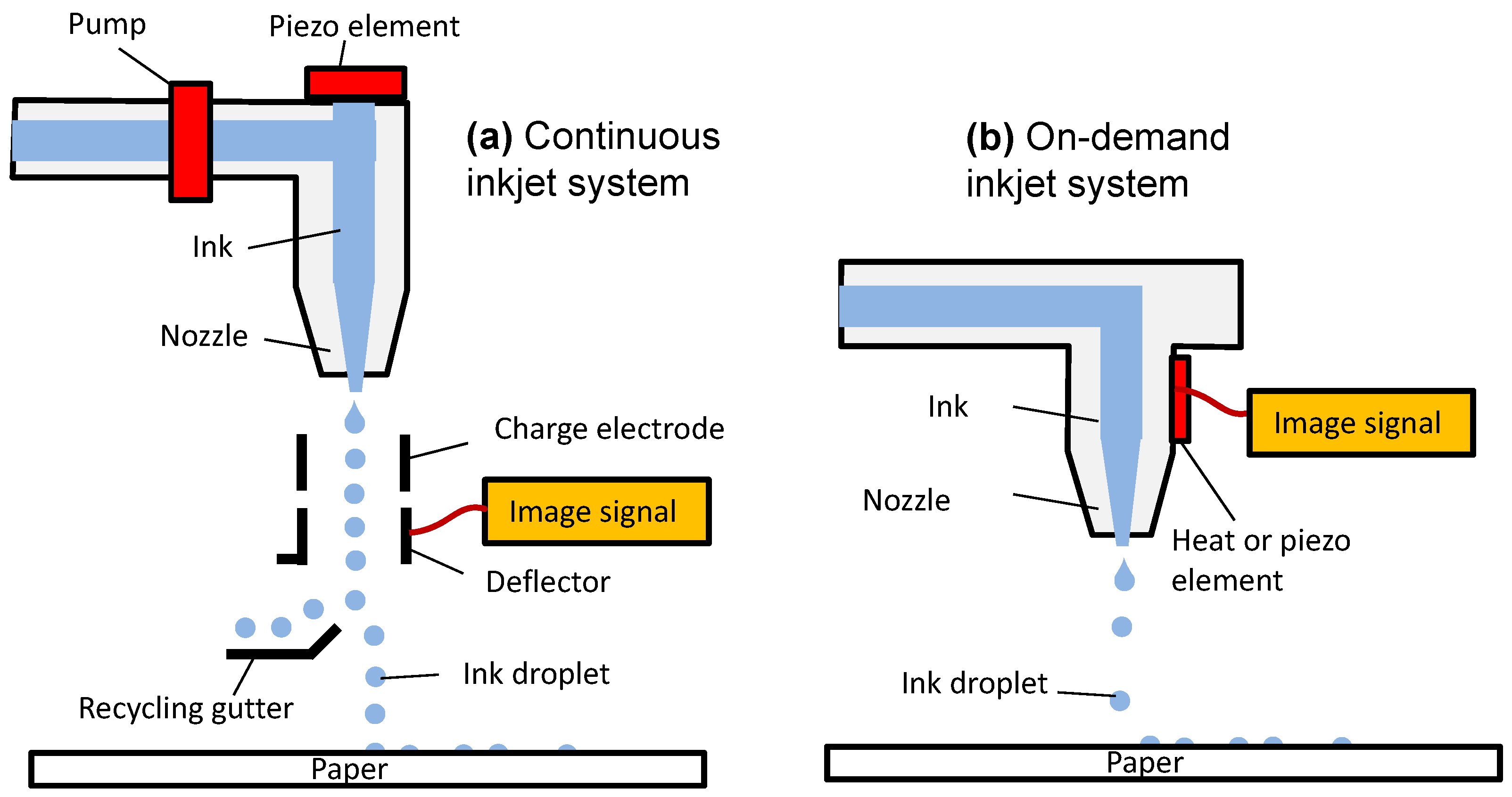
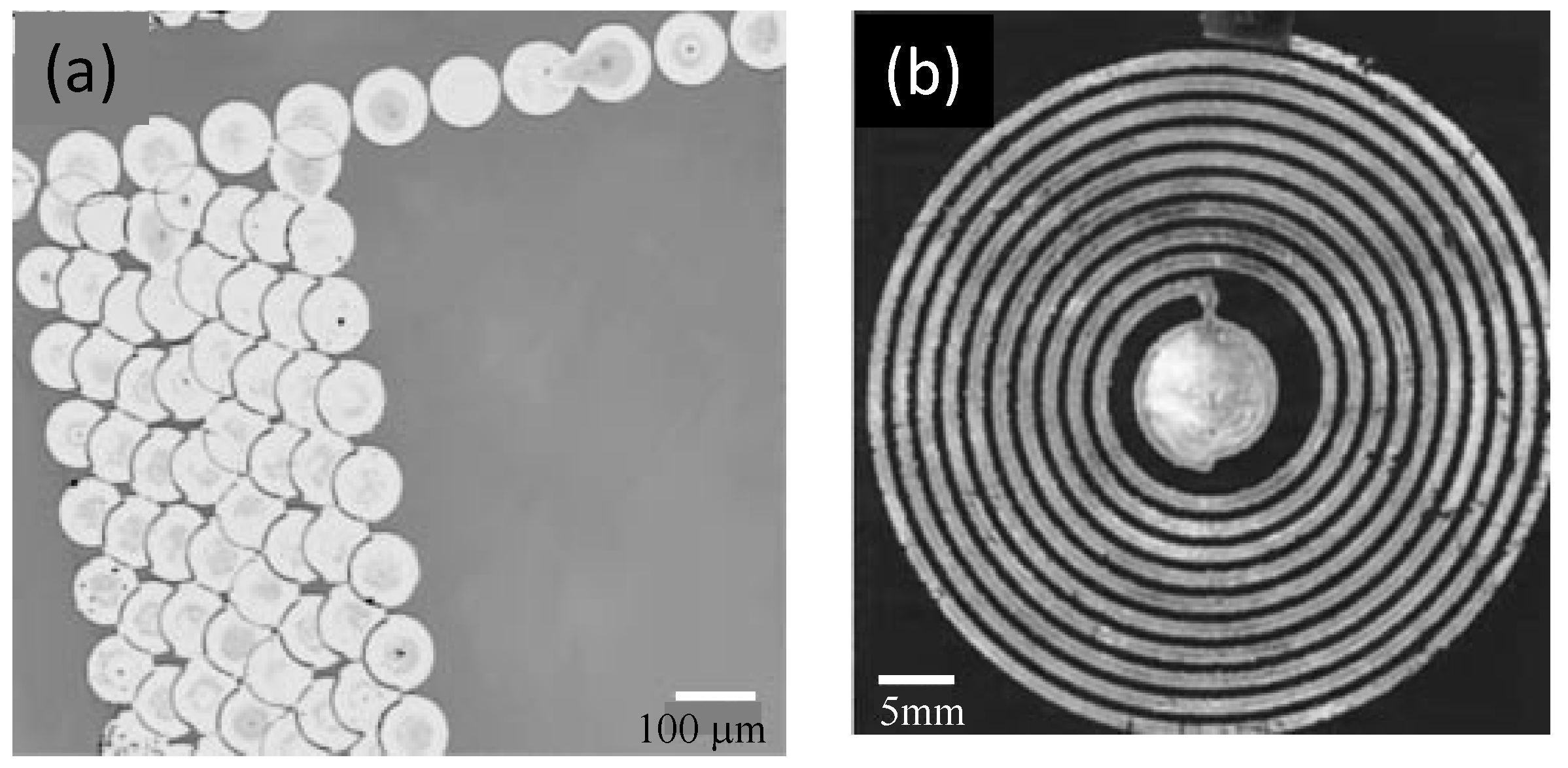
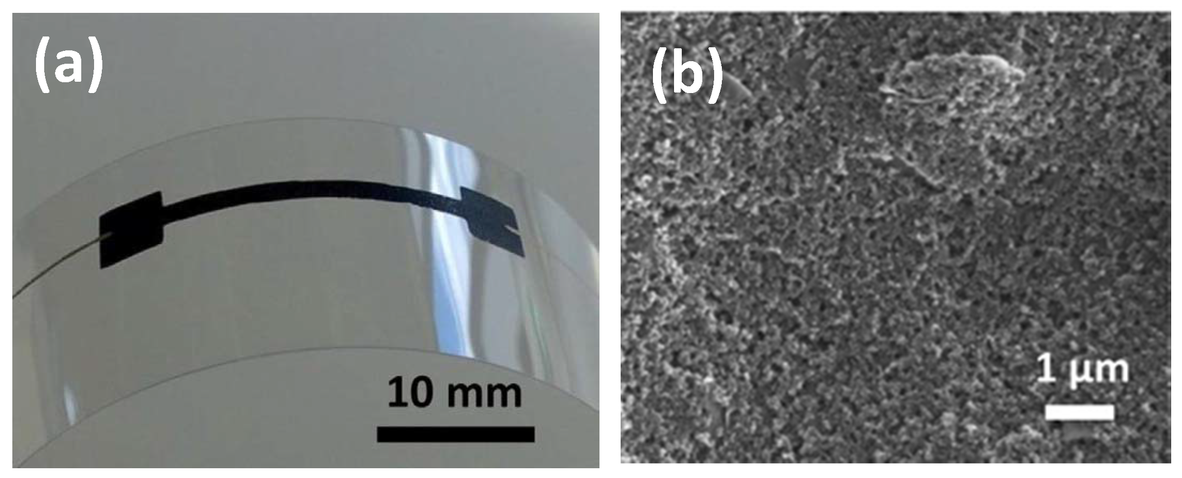
2. Printing Methods
3. Printable Materials
3.1. Conductive Materials
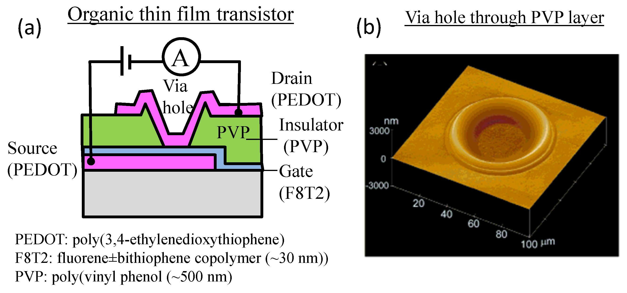
3.2. Insulator Materials
3.3. Sacrificial Materials
3.4. Piezoelectric Materials
3.5. Other Functional Materials
4. Printed MEMS Devices
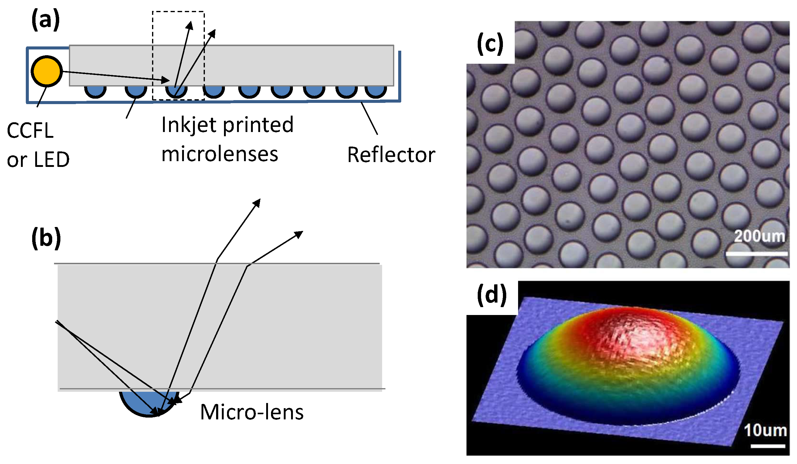
4.1. Microlens
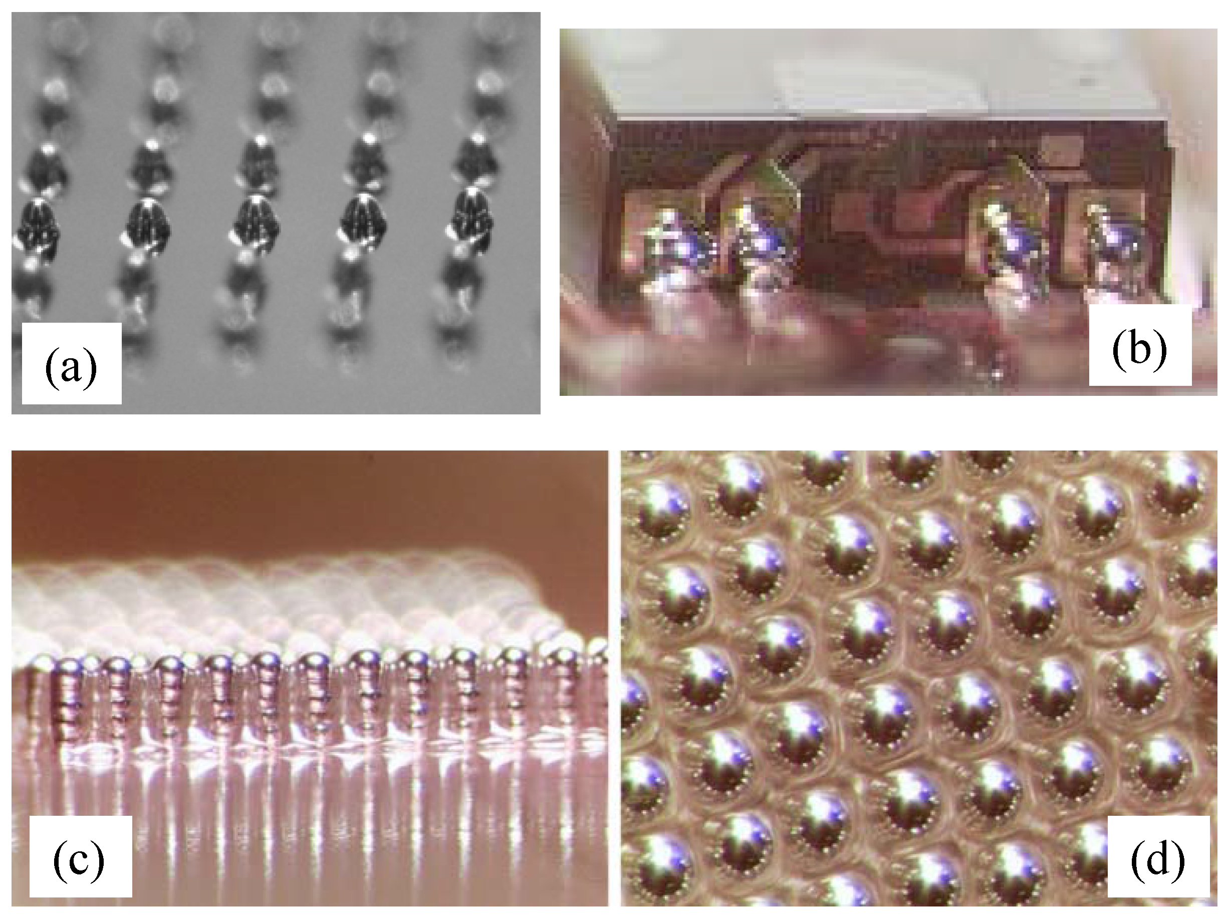
4.2. Solder Bump
4.3. Conductor
4.4. Resistance Temperature Detector
4.5. Strain Gauge
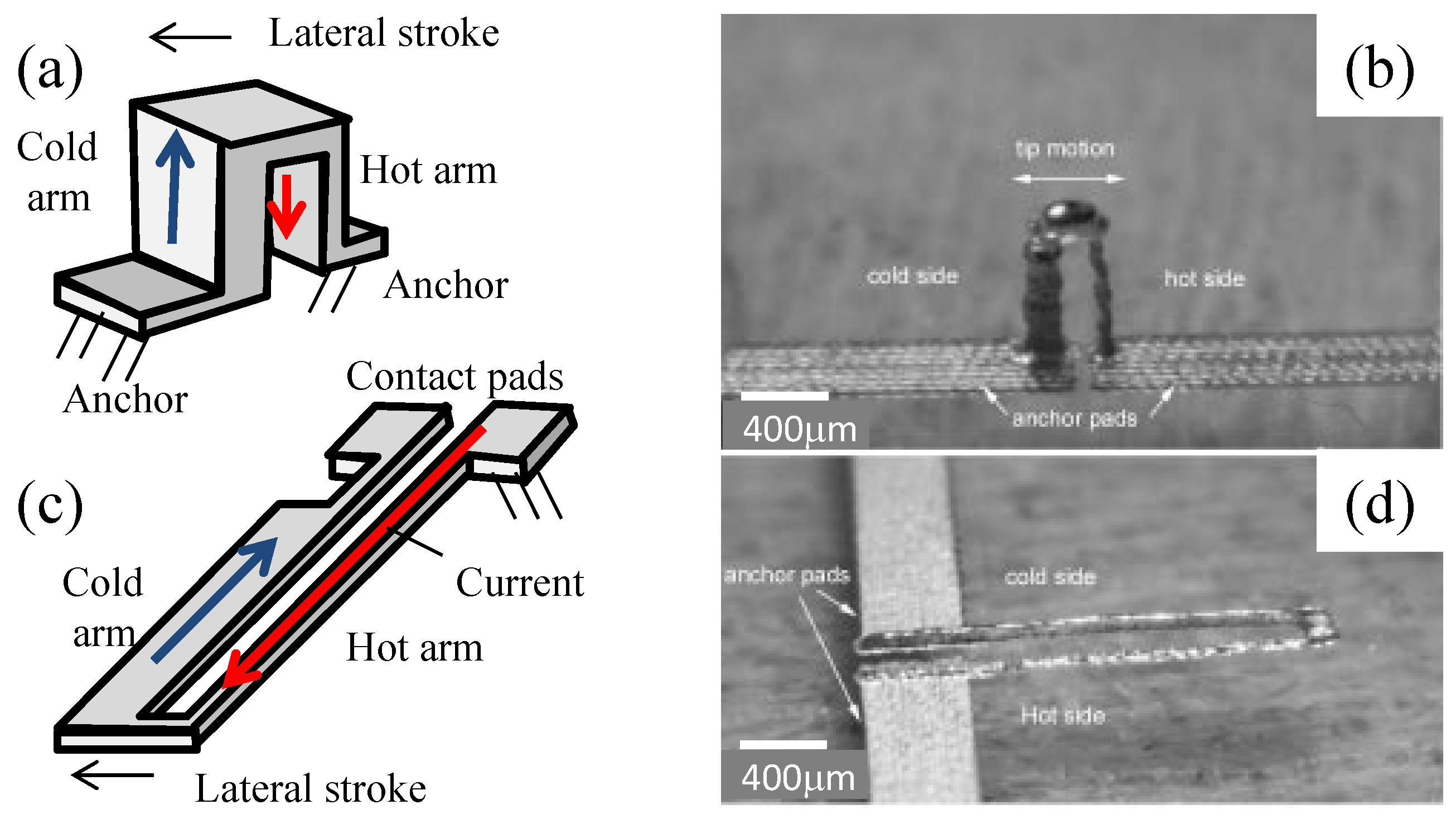
4.6. Heat Actuator
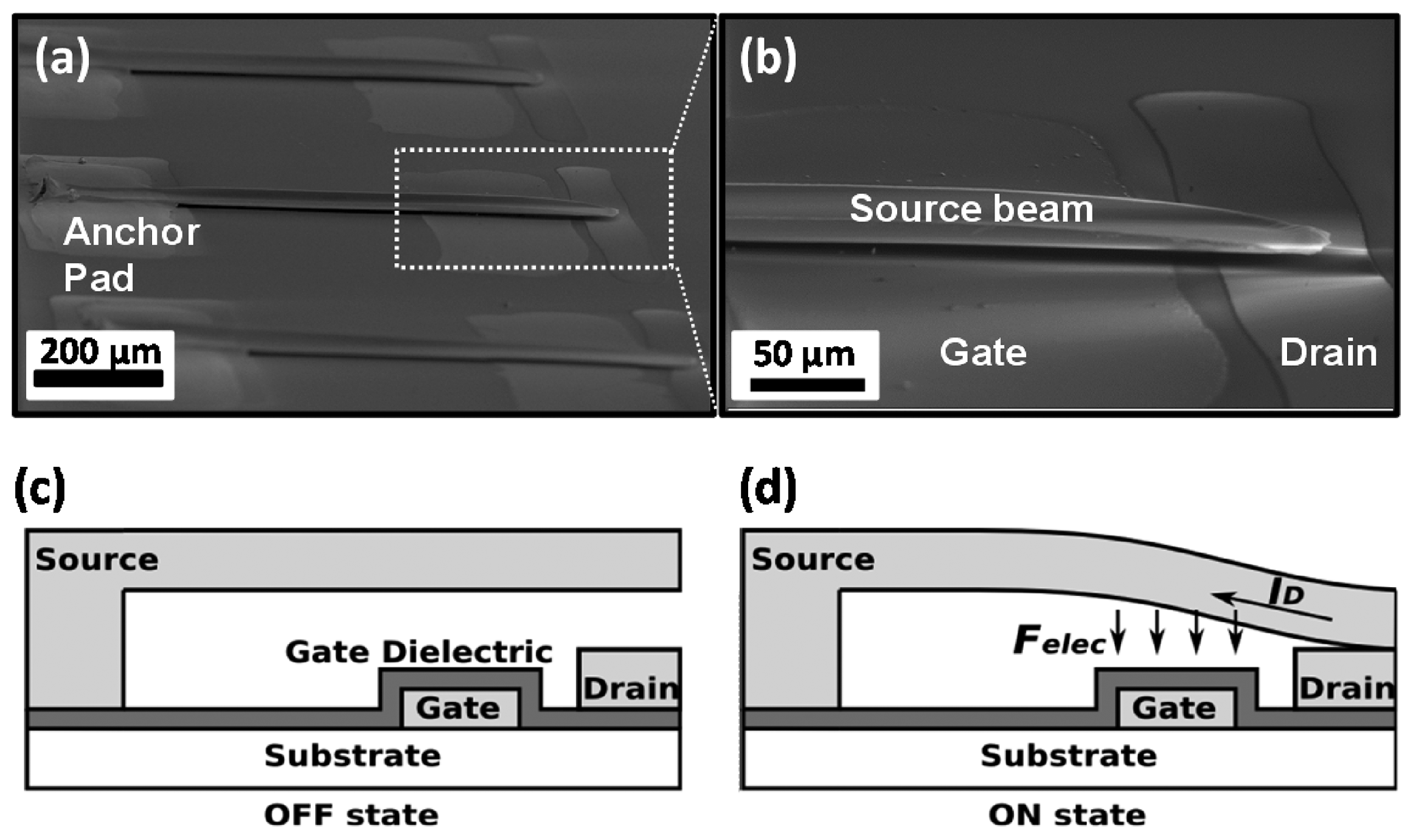
4.7. Air-Gap Electrostatic Switch
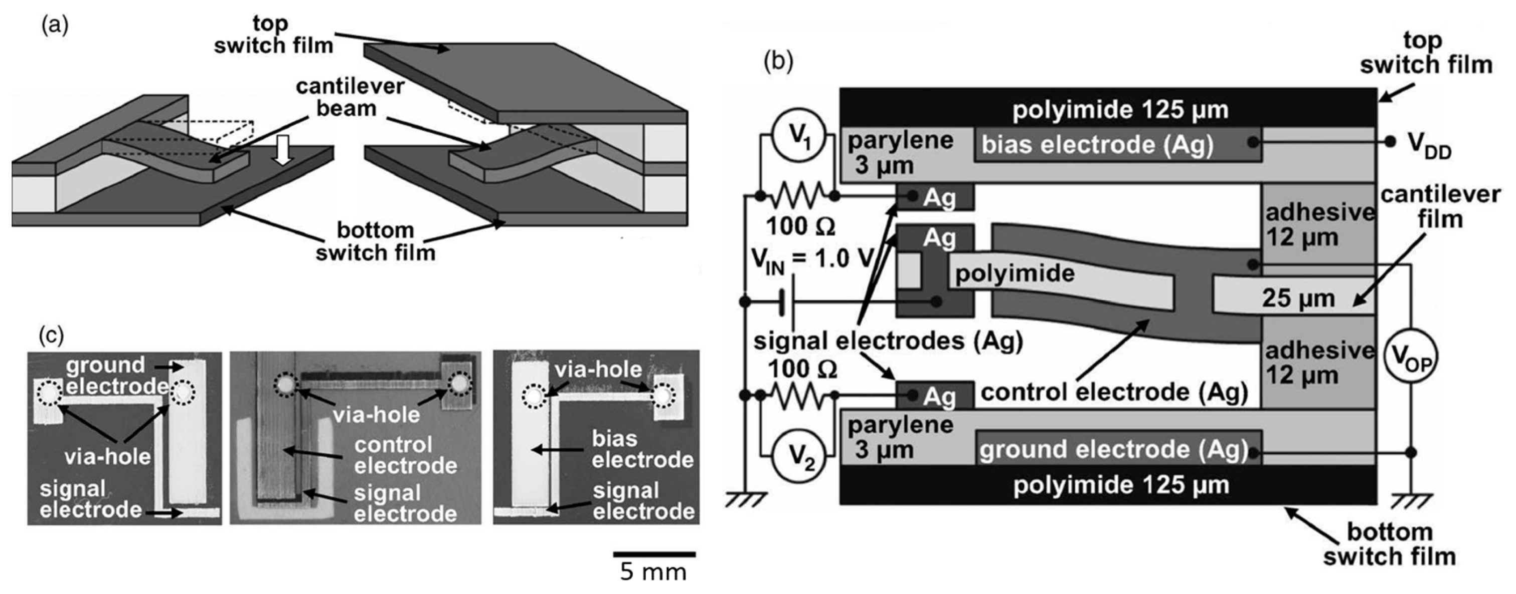
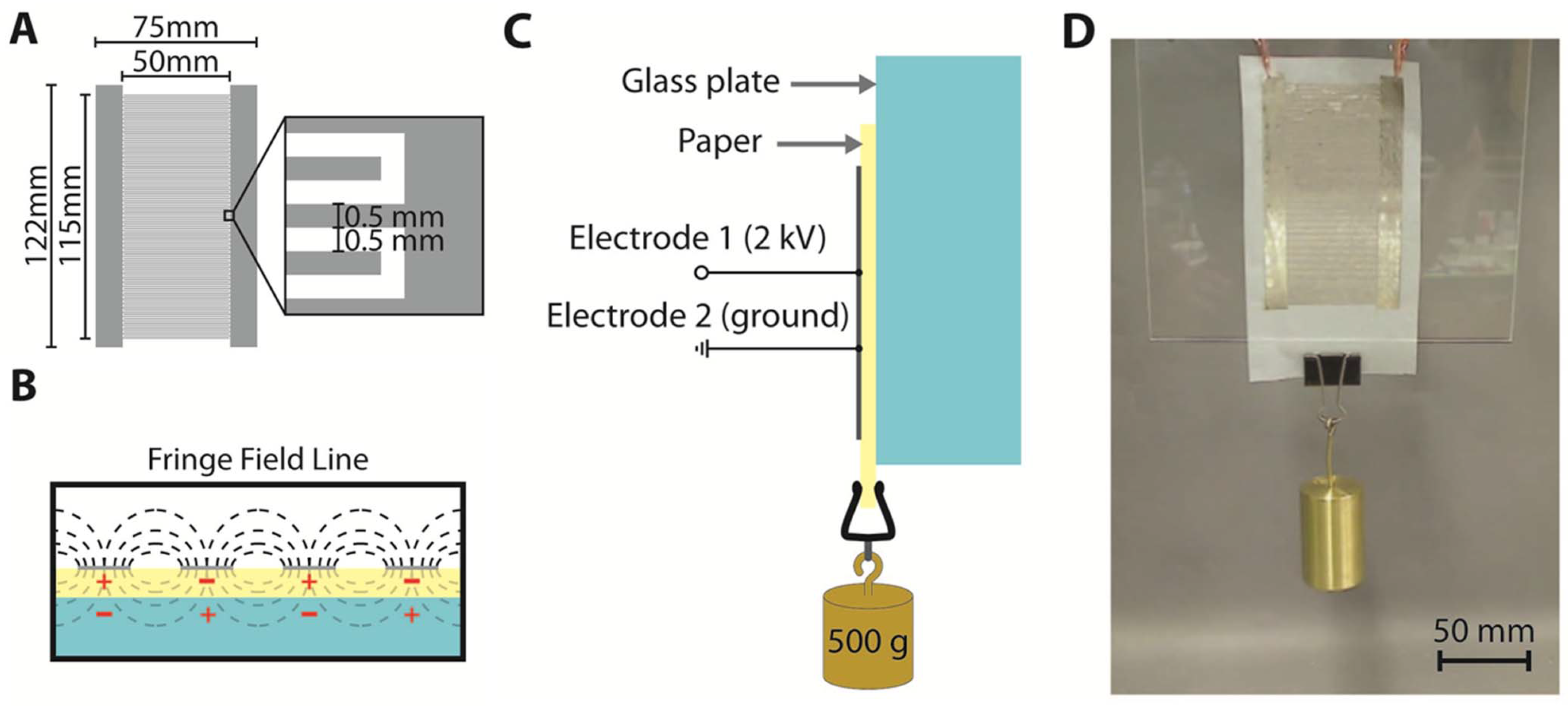
4.8. Electro-Adhesion Pad
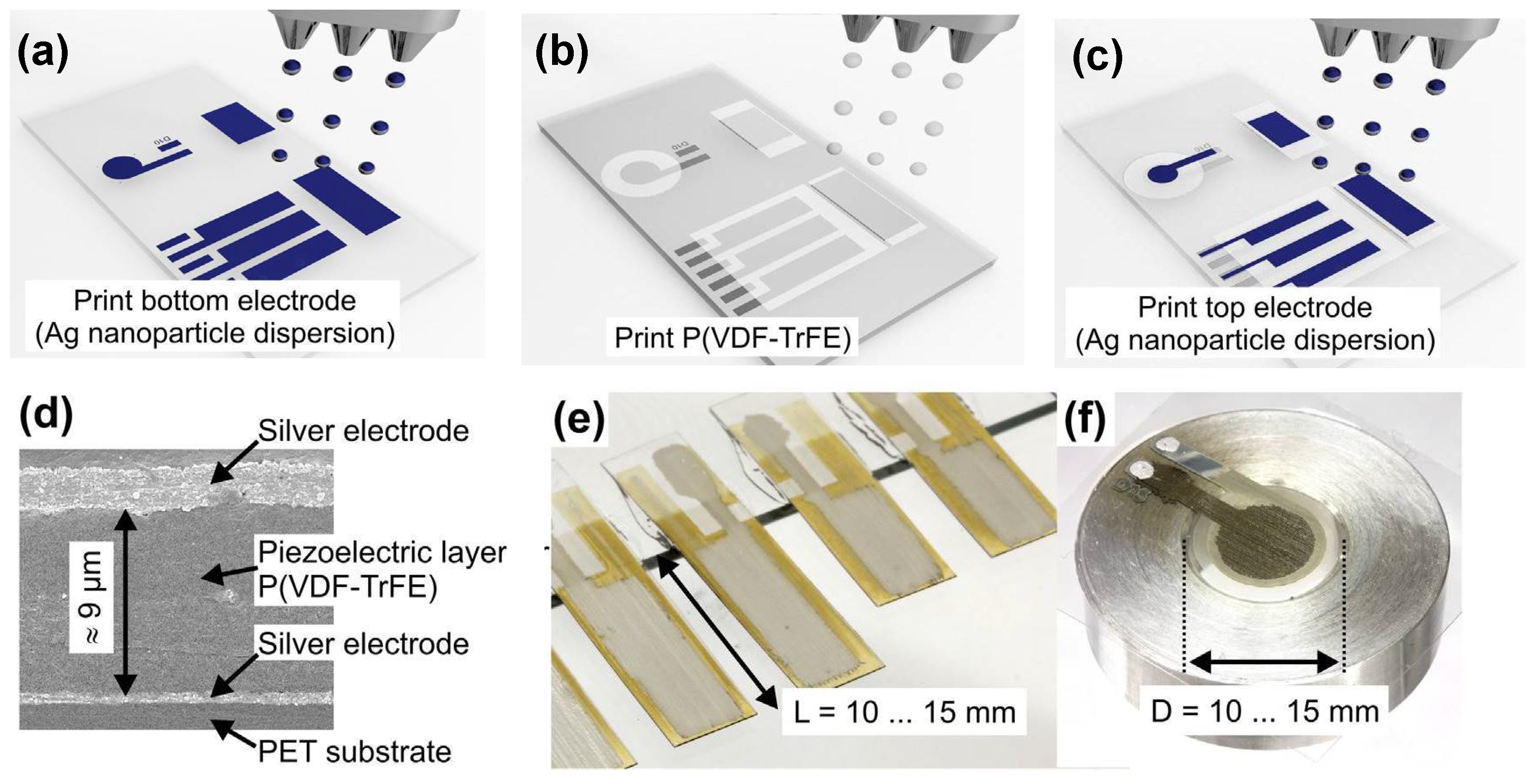
4.9. Piezoelectric Polymer Actuators
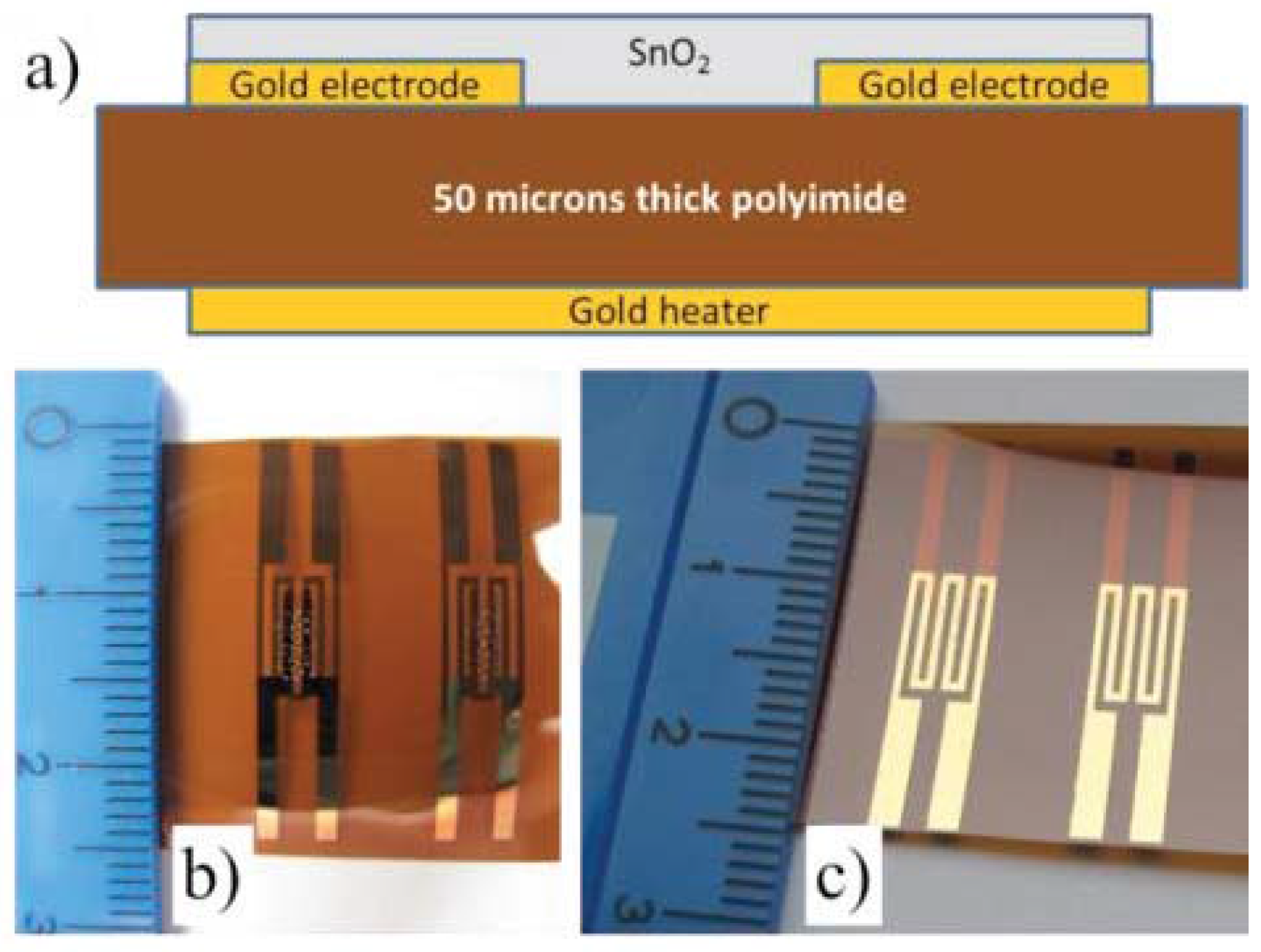
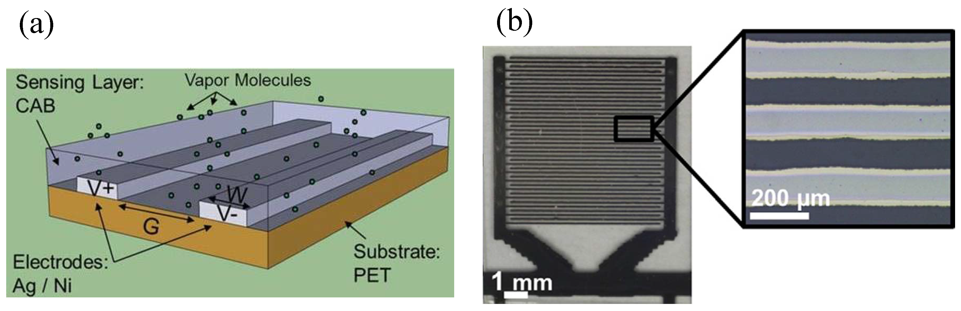
4.10. Gas and Humidity Sensors
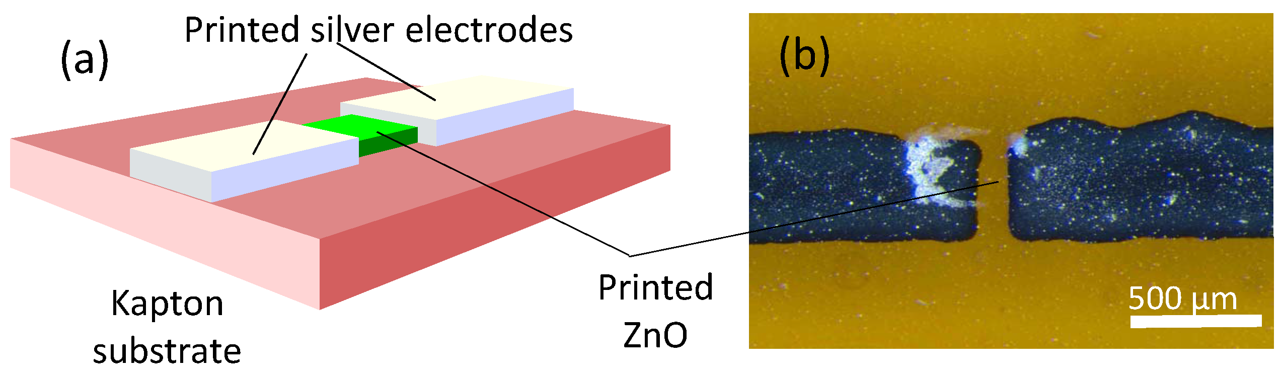
4.11. Photo-Detector for Irradiation
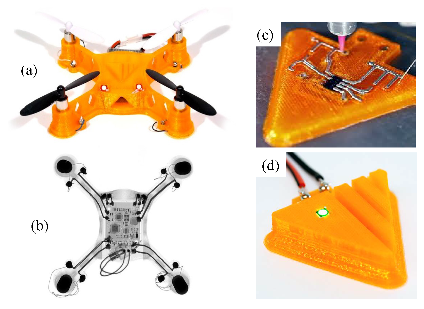
5. Potential Applications
6. Challenges and Prospects
Acknowledgments
Author Contributions
Conflicts of Interest
References
- Maluf, N.; Williams, K. Introduction to Microelectromechanical Systems Engineering; Artech House: Norwood, MA, USA, 2004. [Google Scholar]
- Liu, C. Foundations of MEMS, 1st ed.; Pearson Education Asia: Singapore, 2012; pp. 1–27. [Google Scholar]
- Kovacs, G.T. Micromachined Transducers Sourcebook; WCB/McGraw-Hill New York: Singapore, 1998. [Google Scholar]
- Le, H.P. Progress and trends in ink-jet printing technology. J. Imaging Sci. Technol. 1998, 42, 49–62. [Google Scholar]
- Calvert, P. Inkjet printing for materials and devices. Chem. Mater. 2001, 13, 3299–3305. [Google Scholar] [CrossRef]
- Fuller, S.B.; Wilhelm, E.J.; Jacobson, J.M. Ink-jet printed nanoparticle microelectromechanical systems. J. Microelectromech. Syst. 2002, 11, 54–60. [Google Scholar] [CrossRef]
- Wallace, D.; Hayes, D.; Chen, T.; Shah, V.; Radulescu, D.; Cooley, P.; Wachtler, K.; Nallani, A. Ink-jet as a MEMS manufacturing tool. In Proceedings of the 2007 First International Conference on Integration and Commercialization of Micro and Nanosystems, Hainan, China, 10–13 January 2007; pp. 1161–1168. [Google Scholar]
- Tien, C.H.; Hung, C.H.; Yu, T.H. Microlens arrays by direct-writing inkjet print for LCD backlighting applications. J. Disp. Technol. 2009, 5, 147–151. [Google Scholar] [CrossRef]
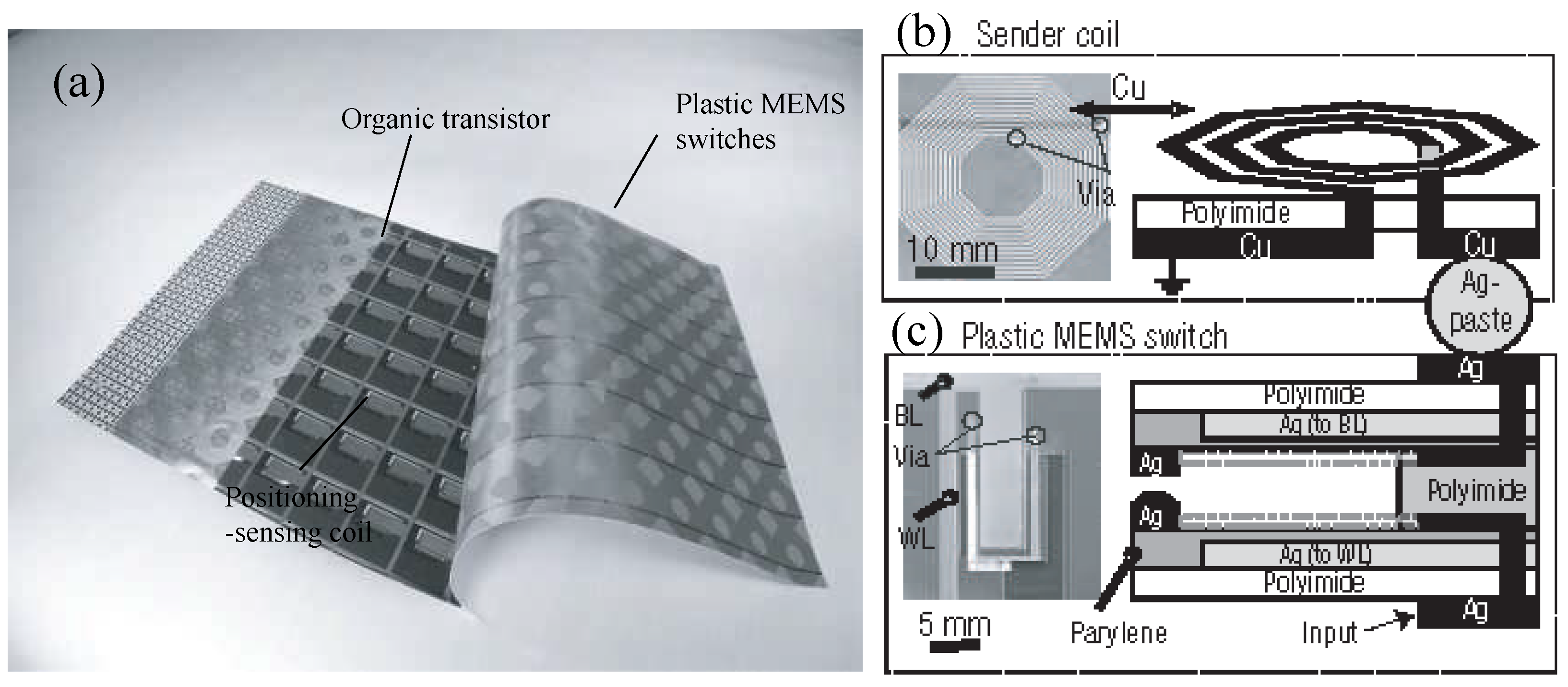
- Sekitani, T.; Takamiya, M.; Noguchi, Y.; Nakano, S.; Kato, Y.; Sakurai, T.; Someya, T. A large-area wireless power-transmission sheet using printed organic transistors and plastic MEMS switches. Nat. Mater. 2007, 6, 413–417. [Google Scholar] [CrossRef] [PubMed]
- Lessing, J.; Glavan, A.C.; Walker, S.B.; Keplinger, C.; Lewis, J.A.; Whitesides, G.M. Inkjet printing of conductive inks with high lateral resolution on omniphobic “RF paper” for paper-based electronics and MEMS. Adv. Mater. 2014, 26, 4677–4682. [Google Scholar] [CrossRef] [PubMed]
- Bessonov, A.; Kirikova, M. Flexible and printable sensors. Nanotechnol. Russ. 2015, 10, 165–180. [Google Scholar] [CrossRef]
- Digial Print Preservation Portal (D3P) Ink jet technology. Available online: http://www.dp3project.org/technologies/digital-printing/inkjet (accessed on 21 March 2017).
- Mackley, M. Ink Jet Rheology. Available online: http://www.malcolmmackley.com/rheology/ink-jet-rheology/ (accessed on 21 March 2017).
- Houben, R.J. Equipment for Printing of High Viscosity Liquids and Molten Metals. Ph.D Thesis, University of Twente, Enschede, The Netherlands, 27 September 2012. [Google Scholar]
- Gale, B.K.; Eddings, M.A.; Sundberg, S.O.; Hatch, A.; Kim, J.K.; Ho, T. Fabrication and packaging: Low-cost MEMS technologies. In Comprehensive Microsystems, 1st ed.; Gianchandani, Y.B., Osamu Tabata, H.Z., Eds.; Elsevier: Amsterdam, The Netherlands, 2008. [Google Scholar]
- Courbat, J.; Kim, Y.; Briand, D.; De Rooij, N. Inkjet printing on paper for the realization of humidity and temperature sensors. In Proceedings of the 16th International IEEE Conference on Solid-State Sensors, Actuators and Microsystems (TRANSDUCERS), Beijing, China, 5–9 June 2011; pp. 1356–1359. [Google Scholar]
- Kawase, T.; Sirringhaus, H.; Friend, R.H.; Shimoda, T. Inkjet printed via-hole interconnections and resistors for all-polymer transistor circuits. Adv. Mater. 2001, 13, 1601. [Google Scholar] [CrossRef]
- Ko, S.H.; Chung, J.; Hotz, N.; Nam, K.H.; Grigoropoulos, C.P. Metal nanoparticle direct inkjet printing for low-temperature 3D micro metal structure fabrication. J. Micromech. Microeng. 2010, 20, 125010. [Google Scholar] [CrossRef]
- Pabst, O.; Perelaer, J.; Beckert, E.; Schubert, U.S.; Eberhardt, R.; Tünnermann, A. All inkjet-printed piezoelectric polymer actuators: Characterization and applications for micropumps in lab-on-a-chip systems. Org. Electron. 2013, 14, 3423–3429. [Google Scholar] [CrossRef]
- Tran, V.T.; Wei, Y.; Yang, H.; Zhan, Z.; Du, H. All-inkjet-printed flexible ZnO micro photodetector for a wearable UV monitoring device. Nanotechnology 2017, 28, 095204. [Google Scholar] [CrossRef] [PubMed]
- Park, E.S.; Chen, Y.; Liu, T.J.K.; Subramanian, V. A new switching device for printed electronics: Inkjet-printed microelectromechanical relay. Nano Lett. 2013, 13, 5355–5360. [Google Scholar] [CrossRef] [PubMed]
- Teng, K.; Vest, R.W. Metallization of solar cells with ink jet printing and silver metallo-organic inks. IEEE Trans. Compon. Hybrids Manuf. Technol. 1988, 11, 291–297. [Google Scholar] [CrossRef]
- Schlaak, H.F.; Jungmann, M.; Matysek, M.; Lotz, P. Novel multilayer electrostatic solid state actuators with elastic dielectric. In Proceedings of the Smart Structures and Materials 2005: Electroactive Polymer Actuators and Devices (EAPAD), San Diego, CA, USA, 6 March 2005; pp. 121–133. [Google Scholar]
- Setiadi, D.; Binnie, T.D.; Regtien, P.; Wubbenhorst, M. Poling of VDF/TrFE copolymers using a step-wise method. In Proceedings of the 9th International Symposium on Electrets (ISE 9), Shanghai, China, 27 September 1996; pp. 831–835. [Google Scholar]
- Ramadan, K.S.; Sameoto, D.; Evoy, S. A review of piezoelectric polymers as functional materials for electromechanical transducers. Smart Mater. Struct. 2014, 23, 033001. [Google Scholar] [CrossRef]
- Zhu, W.; Wang, Z.; Zhang, Z. A trapezoidal bending piezoelectric multilayer actuator by screen printing technology. Ferroelectrics 2001, 263, 167–172. [Google Scholar] [CrossRef]
- Chen, Z.; Song, X.; Lei, L.; Chen, X.; Fei, C.; Chiu, C.T.; Qian, X.; Ma, T.; Yang, Y.; Shung, K.; et al. 3D printing of piezoelectric element for energy focusing and ultrasonic sensing. Nano Energy 2016, 27, 78–86. [Google Scholar] [CrossRef]
- Wang, Z.; Zhu, W.; Zhao, C.; Tan, O.K. Dense PZT thick films derived from sol-gel based nanocomposite process. Mater. Sci. Eng. B 2003, 99, 56–62. [Google Scholar] [CrossRef]
- Wang, C.T.; Huang, K.Y.; Lin, D.T.; Liao, W.C.; Lin, H.W.; Hu, Y.C. A flexible proximity sensor fully fabricated by inkjet printing. Sensors 2010, 10, 5054–5062. [Google Scholar] [CrossRef] [PubMed]
- Wang, Z.; Lau, G.K.; Zhu, W.; Chao, C. Influence of test capacitor features on piezoelectric and dielectric measurement of ferroelectric films. IEEE Trans. Ultrasonics Ferroelectr. Freq. Control 2006, 53, 15–22. [Google Scholar] [CrossRef]
- Wang, D.; Zhu, X.; Liang, J.; Ren, T.; Zha, W.; Dong, W.; Rocks, S.A.; Dorey, R.A.; Xu, Z.; Wang, X. Electrohydrodynamic jet printing of PZT thick film micro-scale structures. J. Eur. Ceram. Soc. 2015, 35, 3475–3483. [Google Scholar] [CrossRef]
- Fujitsuka, N.; Sakata, J.; Miyachi, Y.; Mizuno, K.; Ohtsuka, K.; Taga, Y.; Tabata, O. Monolithic pyroelectric infrared image sensor using PVDF thin film. Sens. Actuators A Phys. 1998, 66, 237–243. [Google Scholar] [CrossRef]
- Holz, S.; Kiricenko, S.; Rissing, L. Integration of PVDF (polyvinylidene fluoride) in MEMS production. ECS Trans. 2014, 64, 189–195. [Google Scholar] [CrossRef]
- Setiadi, D.; Regtien, P.; Sarro, P. Realization of an integrated VDF/TrFE copolymer-on-silicon pyroelectric sensor. Microelectron. Eng. 1995, 29, 85–88. [Google Scholar] [CrossRef]
- Cox, W.R.; Guan, C.; Hayes, D.J.; Wallace, D.B. Microjet printing of micro-optical interconnects. IEPS J. 2000, 23, 346–351. [Google Scholar]
- Fakhfouri, V.; Cantale, N.; Mermoud, G.; Kim, J.; Boiko, D.; Charbon, E.; Martinoli, A.; Brugger, J. Inkjet printing of SU-8 for polymer-based MEMS a case study for microlenses. In Proceedings of the IEEE 21st International Conference on Micro Electro Mechanical Systems, Wuhan, China, 13–17 January 2008; pp. 407–410. [Google Scholar]
- Wallace, D.B.; Hayes, D.J. Solder Jet Technology. Available online: http://www.microfab.com/electronics-sp-72291006 (accessed on 21 March 2017).
- Bessonov, A.; Kirikova, M.; Haque, S.; Gartseev, I.; Bailey, M.J. Highly reproducible printable graphite strain gauges for flexible devices. Sens. Actuators A Phys. 2014, 206, 75–80. [Google Scholar] [CrossRef]
- Michelis, F.; Bodelot, L.; Bonnassieux, Y.; Lebental, B. Highly reproducible, hysteresis-free, flexible strain sensors by inkjet printing of carbon nanotubes. Carbon 2015, 95, 1020–1026. [Google Scholar] [CrossRef]
- Guckel, H.; Klein, J.; Christenson, T.; Skrobis, K.; Laudon, M.; Lovell, E. Thermo-magnetic metal flexure actuators. In Proceedings of the Technical Digest IEEE Solid-State Sensor and Actuator Workshop, Hilton Head Island, SC, USA, 22–25 June 1992; pp. 73–75. [Google Scholar]
- Comtois, J.H.; Bright, V.M. Surface micromachined polysilicon thermal actuator arrays and applications. In Proceedings of the Solid-State Sensor and Actuator Workshop, Hilton Head, SC, USA, 2–6 June 1996; pp. 174–177. [Google Scholar]
- Huang, Q.A.; Lee, N.K.S. Analysis and design of polysilicon thermal flexure actuator. J. Micromech. Microeng. 1999, 9, 64. [Google Scholar] [CrossRef]
- Yokota, T.; Nakano, S.; Sekitani, T.; Someya, T. Plastic complementary microelectromechanical switches. Appl. Phys. Lett. 2008, 93, 251. [Google Scholar] [CrossRef]
- Monkman, G.; Taylor, P.; Farnworth, G. Principles of electroadhesion in clothing robotics. Int. J. Cloth. Sci. Technol. 1989, 1, 14–20. [Google Scholar] [CrossRef]
- Monkman, G.J. An analysis of astrictive prehension. Int. J. Robot. Res. 1997, 16, 1–10. [Google Scholar] [CrossRef]
- Monkman, G. Electroadhesive microgrippers. Ind. Robot Int. J. 2003, 30, 326–330. [Google Scholar] [CrossRef]
- Prahlad, H.; Pelrine, R.; Stanford, S.; Marlow, J.; Kornbluh, R. Electroadhesive robots – Wall climbing robots enabled by a novel, robust, and electrically controllable adhesion technology. In Proceedings of the IEEE International Conference on Robotics and Automation, Pasadena, CA, USA, 19–23 May 2008; pp. 3028–3033. [Google Scholar]
- Graule, M.; Chirarattananon, P.; Fuller, S.; Jafferis, N.; Ma, K.; Spenko, M.; Kornbluh, R.; Wood, R. Perching and takeoff of a robotic insect on overhangs using switchable electrostatic adhesion. Science 2016, 352, 978–982. [Google Scholar] [CrossRef] [PubMed]
- Shintake, J.; Rosset, S.; Schubert, B.; Floreano, D.; Shea, H. Versatile soft grippers with intrinsic electroadhesion based on multifunctional polymer actuators. Adv. Mater. 2016, 28, 231–238. [Google Scholar] [CrossRef] [PubMed]
- Pabst, O.; Hölzer, S.; Beckert, E.; Perelaer, J.; Schubert, U.S.; Eberhardt, R.; Tünnermann, A. Inkjet printed micropump actuator based on piezoelectric polymers: Device performance and morphology studies. Org. Electron. 2014, 15, 3306–3315. [Google Scholar] [CrossRef]
- Rieu, M.; Camara, M.; Tournier, G.; Viricelle, J.-P.; Pijolat, C.; de Rooij, N.; Briand, D. Fully inkjet printed SnO2 gas sensor on plastic substrate. Sens. Actuators B Chem. 2016, 236, 1091–1097. [Google Scholar] [CrossRef]
- Molina-Lopez, F.; Briand, D.; De Rooij, N. All additive inkjet printed humidity sensors on plastic substrate. Sens. Actuators B Chem. 2012, 166–167, 212–222. [Google Scholar] [CrossRef]
- Molina-Lopez, F.; Quintero, A.V.; Mattana, G.; Briand, D.; De Rooij, N. Large-area compatible fabrication and encapsulation of inkjet-printed humidity sensors on flexible foils with integrated thermal compensation. J. Micromech. Microeng. 2013, 23, 025012. [Google Scholar] [CrossRef]
- Quintero, A.V.; Molina-Lopez, F.; Smits, E.; Danesh, E.; van den Brand, J.; Persaud, K.; Oprea, A.; Barsan, N.; Weimar, U.; de Rooij, N.; et al. Smart rfid label with a printed multisensor platform for environmental monitoring. Flex. Print. Electron. 2016, 1, 025003. [Google Scholar] [CrossRef]
- Kern, J. Machine Design Who’s Who in 3D Printing Electronics. Available online: http://www.machinedesign.com/3d-printing/who-s-who-3d-printing-electronics (accessed on 19 May 2017).
- Owano, N. Beyond the Trinkets: Voxel8 Shows 3D Electronics Printer. Available online: https://techxplore.com/pdf340339915.pdf (accessed on 13 January 2015).
- Voxel8. 3D Printed Quadcopter: Voxel8 Developer’s Kit. Available online: https://www.youtube.com/watch?v=yeAJB_Nl0qc ( accessed on 24 May 2016).
- Lau, G.K.; Chin, Y.W.; Goh, J.T.W.; Wood, R.J. Dipteran-insect-inspired thoracic mechanism with nonlinear stiffness to save inertial power of flapping-wing flight. IEEE Trans. Robot. 2014, 30, 1187–1197. [Google Scholar] [CrossRef]
- Shea, H.R.; Shintake, J.; Floreano, D. SPIE Newsroom: Soft compliant gripper for safe manipulation of extremely fragile objects. Available online: http://doi.org/10.1117/2.1201603.006409 (accessed on 11 May 2016).
- Optomec. AEROSOL JET 5X SYSTEM. Available online: https://www.optomec.com/wp-content/uploads/2014/04/AJ5X_System_Web3-17.pdf (accessed on 21 March 2017).
- Lau, G.; Goosen, J.; Van Keulen, F.; French, P.; Sarro, P. Actuated elastomers with rigid vertical electrodes. J. Micromech. Microeng. 2006, 16, S35. [Google Scholar] [CrossRef]
- Khoo, Z.X.; Teoh, J.E.M.; Liu, Y.; Chua, C.K.; Yang, S.; An, J.; Leong, K.F.; Yeong, W.Y. 3D printing of smart materials: A review on recent progresses in 4D printing. Virtual Phys. Prototyp. 2015, 10, 103–122. [Google Scholar] [CrossRef]
- Leist, S.K.; Zhou, J. Current status of 4D printing technology and the potential of light-reactive smart materials as 4D printable materials. Virtual Phys. Prototyp. 2016, 11, 249–262. [Google Scholar] [CrossRef]
- Saengchairat, N.; Tran, T.; Chua, C.K. A review: Additive manufacturing for active electronic components. Virtual Phys. Prototyp. 2017, 12, 31–46. [Google Scholar] [CrossRef]


© 2017 by the authors. Licensee MDPI, Basel, Switzerland. This article is an open access article distributed under the terms and conditions of the Creative Commons Attribution (CC BY) license (http://creativecommons.org/licenses/by/4.0/).
Share and Cite
Lau, G.-K.; Shrestha, M. Ink-Jet Printing of Micro-Electro-Mechanical Systems (MEMS). Micromachines 2017, 8, 194. https://doi.org/10.3390/mi8060194
Lau G-K, Shrestha M. Ink-Jet Printing of Micro-Electro-Mechanical Systems (MEMS). Micromachines. 2017; 8(6):194. https://doi.org/10.3390/mi8060194
Chicago/Turabian StyleLau, Gih-Keong, and Milan Shrestha. 2017. "Ink-Jet Printing of Micro-Electro-Mechanical Systems (MEMS)" Micromachines 8, no. 6: 194. https://doi.org/10.3390/mi8060194
APA StyleLau, G.-K., & Shrestha, M. (2017). Ink-Jet Printing of Micro-Electro-Mechanical Systems (MEMS). Micromachines, 8(6), 194. https://doi.org/10.3390/mi8060194