
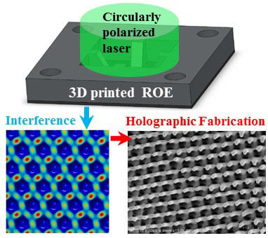
Flexible Holographic Fabrication of 3D Photonic Crystal Templates with Polarization Control through a 3D Printed Reflective Optical Element

 ,
, 
Abstract
:
1. Introduction
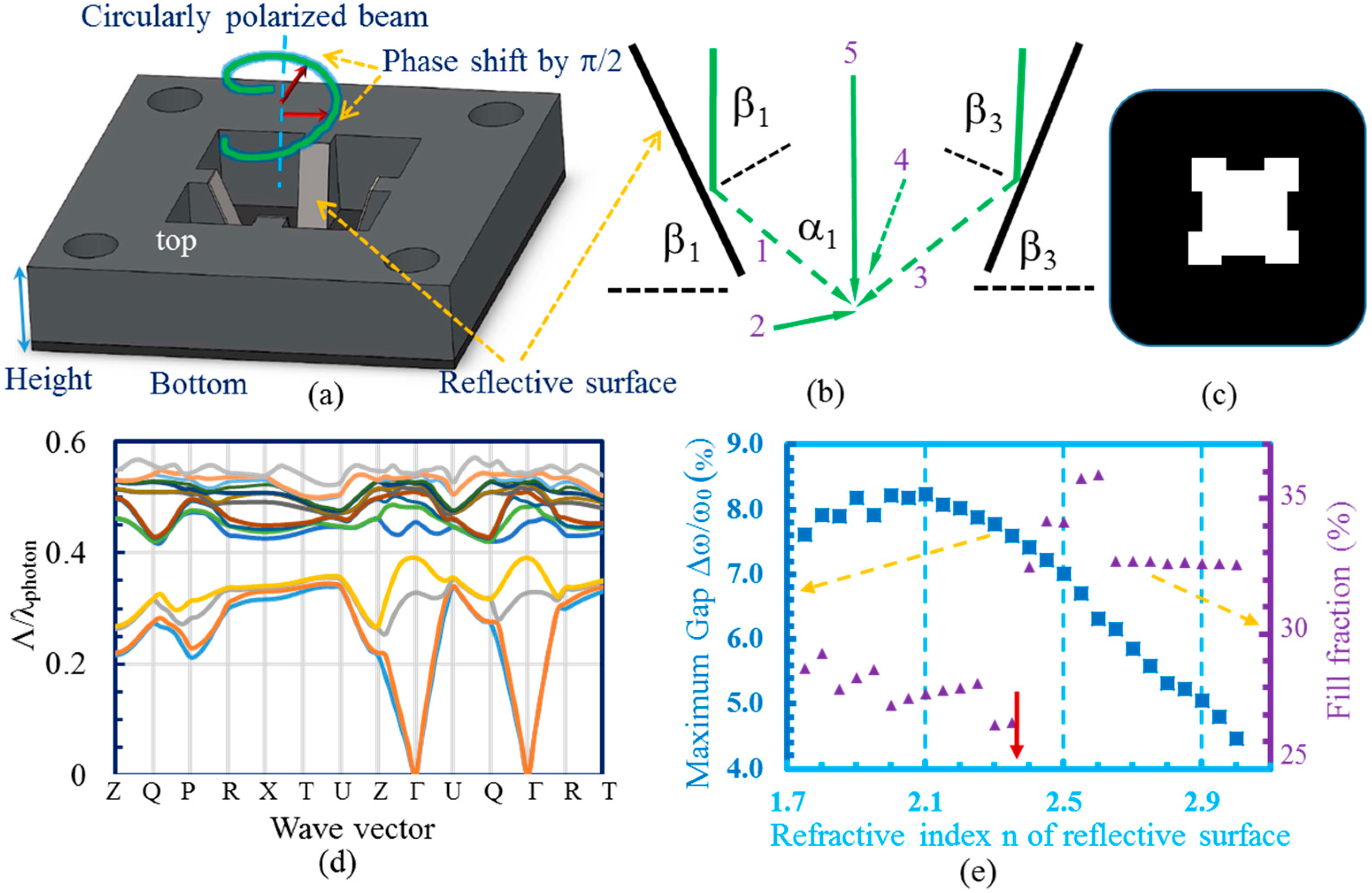
2. Experiments
3. Simulation Results
4. Experimental Results
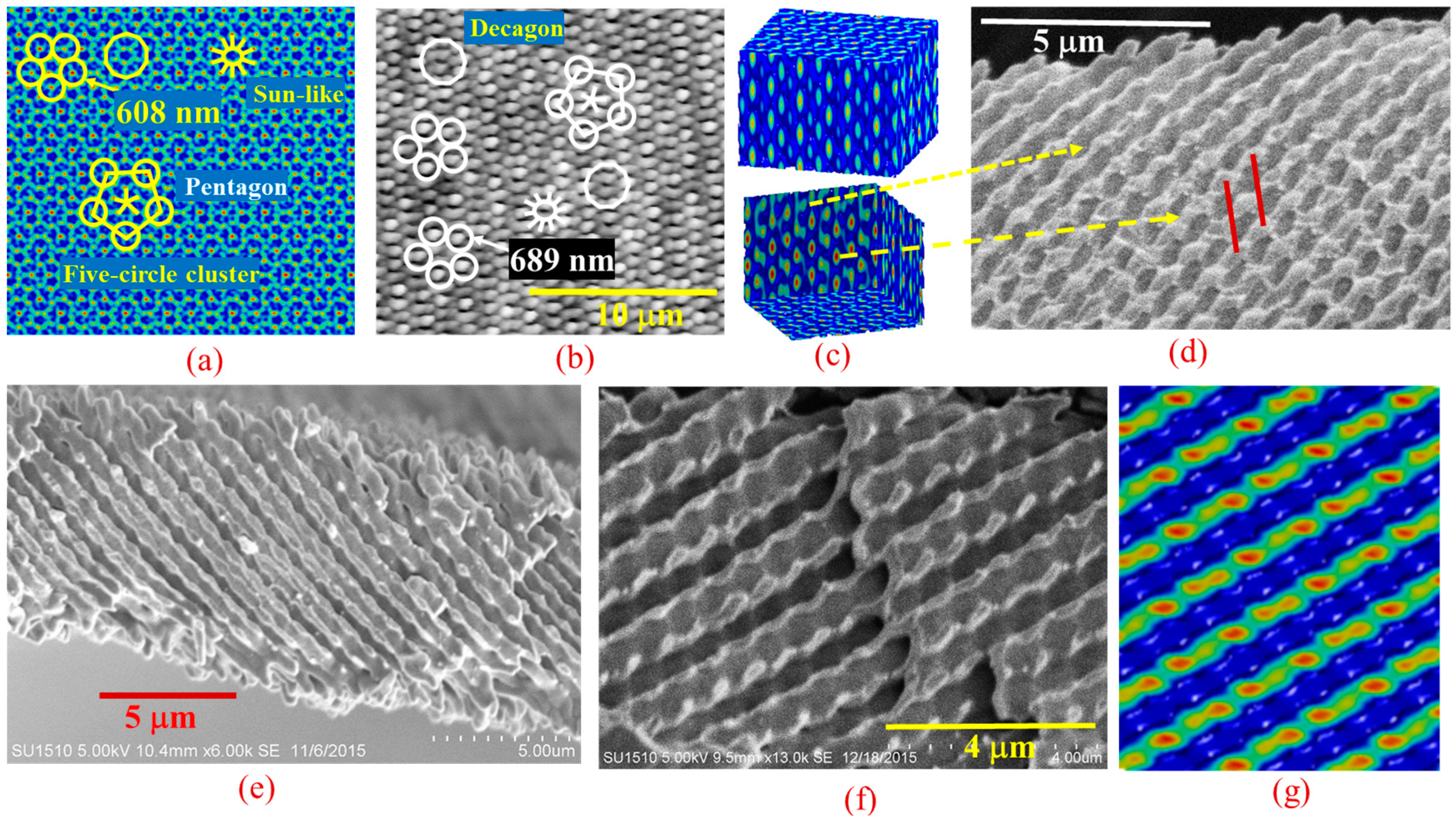
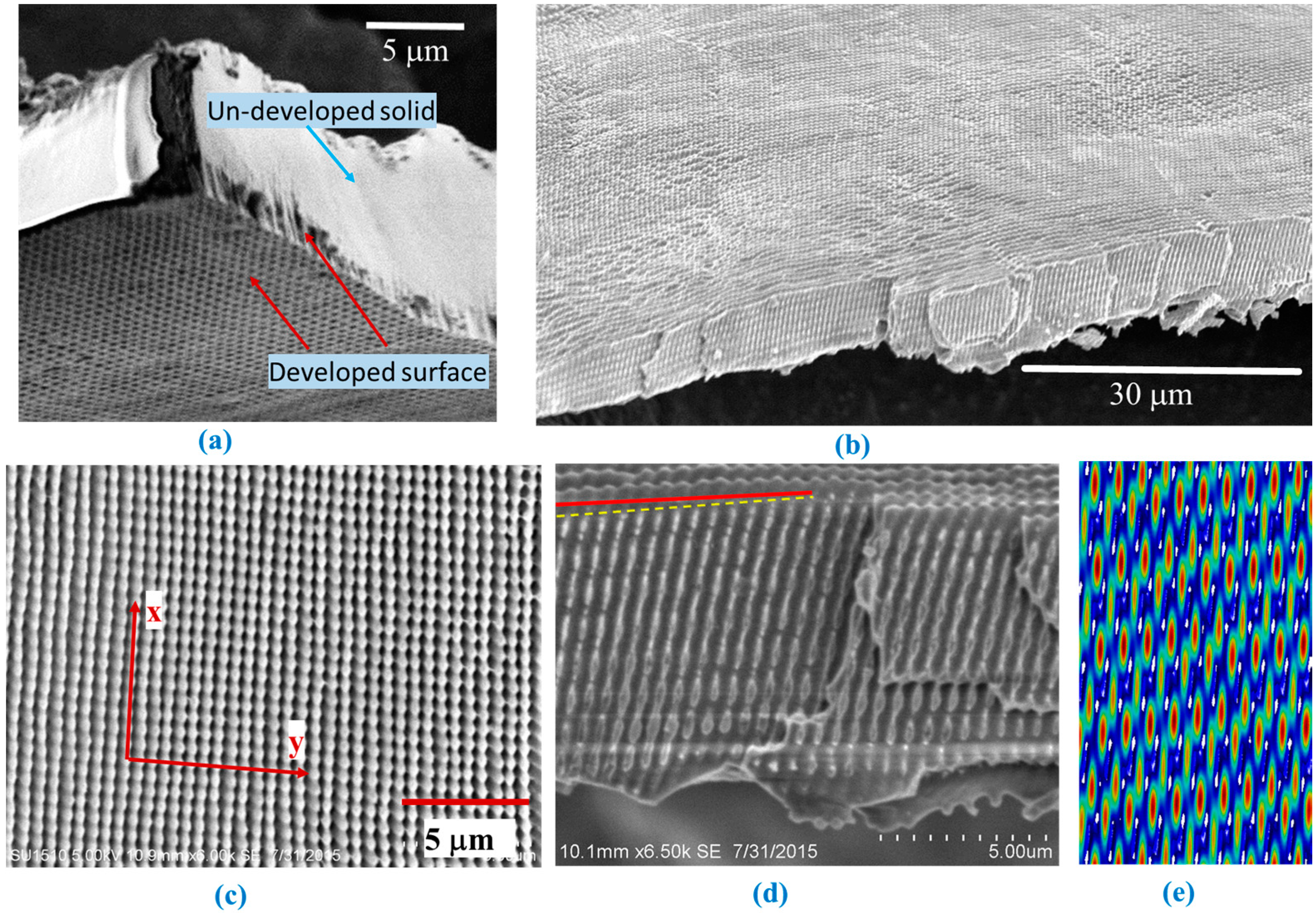
4.1. Fabrication of 3D Structures through Multi-Beam 4 + 1 Interference
4.2. Fabrication of Quasi-Crystals through Multi-Beam 5 + 1 Interference
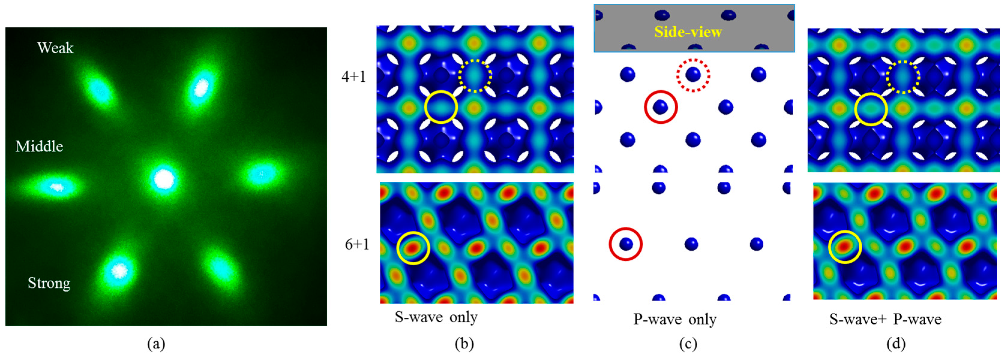
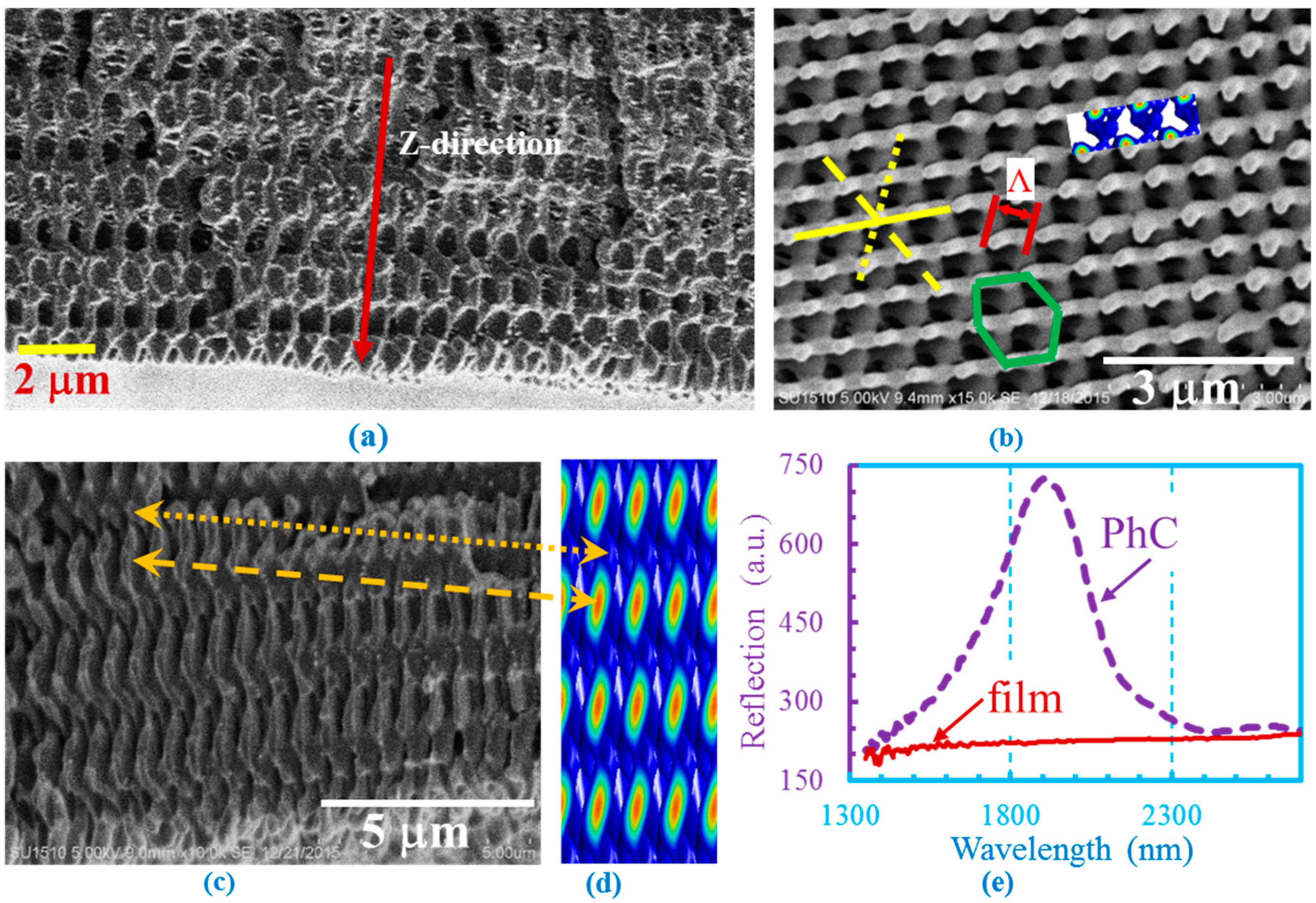
4.3. Holographic Fabrication Using ROE for Multiple Beam 6 + 1 Interference
5. Discussion
6. Conclusions
Acknowledgments
Author Contributions
Conflicts of Interest
References
- Tandaechanurat, A.; Ishida, S.; Guimard, D.; Nomura, M.; Iwamoto, S.; Arakawa, Y. Lasing oscillation in a three-dimensional photonic crystal nanocavity with a complete bandgap. Nat. Photonics 2011, 5, 91–94. [Google Scholar] [CrossRef]
- Qi, M.; Lidorikis, E.; Rakich, P.T.; Johnson, S.G.; Joannopoulos, J.D.; Ippen, E.P.; Smith, H.I. A three-dimensional optical photonic crystal with designed point defects. Nature 2004, 429, 538–542. [Google Scholar] [CrossRef] [PubMed]
- Ergin, T.; Stenger, N.; Brenner, P.; Pendry, J.B.; Wegener, M. Three-dimensional invisibility cloak at optical wavelengths. Science 2010, 328, 337–339. [Google Scholar] [CrossRef] [PubMed]
- Guldin, S.; Hüttner, S.; Kolle, M.; Welland, M.E.; Müller-Buschbaum, P.; Friend, R.H.; Steiner, U.; Tétreault, N. Dye-sensitized solar cell based on a three-dimensional photonic crystal. Nano Lett. 2010, 10, 2303–2309. [Google Scholar] [CrossRef] [PubMed]
- Vlasov, Y.A.; Bo, X.-Z.; Sturm, J.C.; Norris, D.J. On-chip natural assembly of silicon photonic bandgap crystals. Nature 2001, 414, 289–293. [Google Scholar] [CrossRef] [PubMed]
- Jiang, P.; Bertone, J.F.; Colvin, V.L. A Lost-wax approach to monodisperse colloids and their crystals. Science 2001, 291, 453–457. [Google Scholar] [CrossRef] [PubMed]
- Deubel, M.; von Freymann, G.; Wegener, M.; Pereira, S.; Busch, K.; Soukoulis, C.M. Direct laser writing of three-dimensional photonic-crystal templates for telecommunications. Nat. Mater. 2004, 3, 444–447. [Google Scholar] [CrossRef] [PubMed]
- Seet, K.K.; Mizeikis, V.; Matsuo, S.; Juodkazis, S.; Misawa, H. Three-dimensional spiral-architecture photonic crystals obtained by direct laser writing. Adv. Mater. 2005, 17, 541–545. [Google Scholar] [CrossRef]
- Thiel, M.; Rill, M.S.; von Freymann, G.; Wegener, M. Three-Dimensional Bi-chiral photonic crystals. Adv. Mater. 2009, 21, 4680–4682. [Google Scholar] [CrossRef]
- Ledermann, A.; Cademartiri, L.; Hermatschweiler, M.; Toninelli, C.; Ozin, G.A.; Wiersma, D.S.; Wegener, M.; von Freymann, G. Three-dimensional silicon inverse photonic quasicrystals for infrared wavelengths. Nat. Mater. 2006, 5, 942–945. [Google Scholar] [CrossRef] [PubMed]
- Campbell, M.; Sharp, D.N.; Harrison, M.T.; Denning, R.G.; Turberfield, A.J. Fabrication of photonic crystals for the visible spectrum by holographic lithography. Nature 2000, 404, 53–56. [Google Scholar] [PubMed]
- Yang, S.; Megens, M.; Aizenberg, J.; Wiltzius, P.; Chaikin, P.M.; Russel, W.B. Creating periodic three-dimensional structures by multibeam interference of visible laser. Chem. Mater. 2002, 14, 2831–2833. [Google Scholar] [CrossRef]
- Cai, L.Z.; Yang, X.L.; Wang, Y.R. All fourteen Bravais lattices can be formed by interference of four noncoplanar beams. Opt. Lett. 2002, 27, 900–902. [Google Scholar] [CrossRef] [PubMed]
- Chan, T.Y.M.; Toader, O.; John, S. Photonic band-gap formation by optical-phase-mask lithography. Phys. Rev. E 2006, 73, 046610. [Google Scholar] [CrossRef] [PubMed]
- Lin, Y.; Herman, P.R.; Abolghasemi, E.L. Proposed single-exposure holographic fabrication of microsphere-type photonic crystal through phase mask techniques. J. Appl. Phys. 2005, 97, 096102. [Google Scholar] [CrossRef]
- Lin, Y.; Herman, P.R.; Darmawikarta, K. Design and holographic fabrication of tetragonal and cubic photonic crystals with phase mask: Toward the mass-production of three-dimensional photonic crystals. Appl. Phys. Lett. 2005, 86, 071117. [Google Scholar] [CrossRef]
- Lin, Y.; Rivera, D.; Chen, K.P. Woodpile-type photonic crystals with orthorhombic or tetragonal symmetry formed through phase mask techniques. Opt. Express 2006, 14, 887–892. [Google Scholar] [CrossRef] [PubMed]
- Lin, Y.; Harb, A.; Rodriguez, D.; Lozano, K.; Xu, D.; Chen, K.P. Fabrication of two-layer integrated phase mask for single-beam and single-exposure fabrication of three-dimensional photonic crystal. Opt. Express 2008, 16, 9165–9172. [Google Scholar] [CrossRef] [PubMed]
- Harb, A.; Torres, F.; Ohlinger, K.; Lin, Y.; Lozano, K.; Xu, D.; Chen, K.P. Holographically formed three-dimensional Penrose-type photonic quasicrystal through a lab-made single diffractive optical element. Opt. Express 2010, 18, 20512–20517. [Google Scholar] [CrossRef] [PubMed]
- Ohlinger, K.; Zhang, H.; Lin, Y.; Xu, D.; Chen, K.P. A tunable three layer phase mask for single laser exposure 3D photonic crystal generations: Bandgap simulation and holographic fabrication. Opt. Mater. Express 2011, 1, 1034–1039. [Google Scholar] [CrossRef]
- Xu, D.; Chen, K.P.; Ohlinger, K.; Lin, Y. Nanoimprinting lithography of a two-layer phase mask for three-dimensional photonic structure holographic fabrications via single exposure. Nanotechnology 2011, 22, 035303. [Google Scholar] [CrossRef] [PubMed]
- Chanda, D.; Abolghasemi, L.E.; Haque, M.; Ng, M.L.; Herman, P.R. Multi-level diffractive optics for single laser exposure fabrication of telecom-band diamond-like 3-dimensional photonic crystals. Opt. Express 2008, 16, 15402–15414. [Google Scholar] [CrossRef] [PubMed]
- Yuan, L.L.; Herman, P.R. Layered nano-gratings by electron beam writing to form 3-level diffractive optical elements for 3D phase-offset holographic lithography. Nanoscale 2015, 7, 19905–19913. [Google Scholar] [CrossRef] [PubMed]
- Pang, Y.K.; Lee, J.C.; Ho, C.T.; Tam, W.Y. Realization of woodpile structure using optical interference holography. Opt. Express 2006, 14, 9113–9119. [Google Scholar] [CrossRef] [PubMed]
- Wang, X.; Xu, J.; Lee, J.C.; Pang, Y.K.; Tam, W.Y.; Chan, C.T.; Sheng, P. Realization of optical periodic quasicrystals using holographic lithography. Appl. Phys. Lett. 2006, 88, 051901. [Google Scholar] [CrossRef]
- Pang, Y.K.; Lee, J.C.; Lee, H.F.; Tam, W.Y.; Chan, C.T.; Sheng, P. Chiral microstructures (spirals) fabrication by holographic lithography. Opt. Express 2005, 13, 7615–7620. [Google Scholar] [CrossRef] [PubMed]
- Wang, X.; Gao, W.; Hung, J.; Tam, W.Y. Optical activities of large-area SU8 microspirals fabricated by multibeam holographic lithography. Appl. Opt. 2014, 53, 2425–2430. [Google Scholar] [CrossRef] [PubMed]
- Xu, J.; Ma, R.; Wang, X.; Tam, W.Y. Icosahedral quasicrystals for visible wavelengths by optical interference holography. Opt. Express 2007, 15, 4287–4295. [Google Scholar] [CrossRef] [PubMed]
- Xu, D.; Chen, K.P.; Harb, A.; Rodriguez, D.; Lozano, K.; Lin, Y. Phase tunable holographic fabrication for three-dimensional photonic crystal templates by using a single optical element. Appl. Phys. Lett. 2009, 94, 231116. [Google Scholar] [CrossRef]
- George, D.; Lutkenhaus, J.; Lowell, D.; Moazzezi, M.; Adewole, M.; Philipose, U.; Zhang, H.; Poole, Z.L.; Chen, K.P.; Lin, Y. Holographic fabrication of 3D photonic crystals through interference of multi-beams with 4 + 1, 5 + 1 and 6 + 1 configurations. Opt. Express 2014, 22, 22421–22431. [Google Scholar] [CrossRef] [PubMed]
- Lutkenhaus, J.; Lowell, D.; George, D.; Zhang, H.; Lin, Y. Holographic fabrication of designed functional defect lines in photonic crystal lattice using a spatial light modulator. Micromachines 2016, 7, 59. [Google Scholar] [CrossRef]
- Johnson, S.G.; Joannopoulos, J.D. Block-iterative frequency-domain methods for Maxwell’s equations in a planewave basis. Opt. Express 2001, 8, 173–190. [Google Scholar] [CrossRef] [PubMed]
- Oskooi, A.; Favuzzi, P.A.; Tanaka, Y.; Shigeta, H.; Kawakami, Y.; Noda, S. Partially disordered photonic-crystal thin films for enhanced and robust photovoltaics. Appl. Phys. Lett. 2012, 100, 181110. [Google Scholar] [CrossRef]
- Oskooi, A.; De Zoysa, M.; Ishizaki, K.; Noda, S. Experimental demonstration of quasi-resonant absorption in silicon thin films for enhanced solar light trapping. ACS Photonics 2014, 1, 304–309. [Google Scholar] [CrossRef]
- Lutkenhaus, J.; George, D.; Arigong, B.; Zhang, H.; Philipose, U.; Lin, Y. Holographic fabrication of functionally graded photonic lattices through spatially specified phase patterns. Appl. Opt. 2014, 53, 2548–2555. [Google Scholar] [CrossRef] [PubMed]


© 2016 by the authors. Licensee MDPI, Basel, Switzerland. This article is an open access article distributed under the terms and conditions of the Creative Commons Attribution (CC-BY) license ( http://creativecommons.org/licenses/by/4.0/).
Share and Cite
Lowell, D.; George, D.; Lutkenhaus, J.; Tian, C.; Adewole, M.; Philipose, U.; Zhang, H.; Lin, Y. Flexible Holographic Fabrication of 3D Photonic Crystal Templates with Polarization Control through a 3D Printed Reflective Optical Element. Micromachines 2016, 7, 128. https://doi.org/10.3390/mi7070128
Lowell D, George D, Lutkenhaus J, Tian C, Adewole M, Philipose U, Zhang H, Lin Y. Flexible Holographic Fabrication of 3D Photonic Crystal Templates with Polarization Control through a 3D Printed Reflective Optical Element. Micromachines. 2016; 7(7):128. https://doi.org/10.3390/mi7070128
Chicago/Turabian StyleLowell, David, David George, Jeffrey Lutkenhaus, Chris Tian, Murthada Adewole, Usha Philipose, Hualiang Zhang, and Yuankun Lin. 2016. "Flexible Holographic Fabrication of 3D Photonic Crystal Templates with Polarization Control through a 3D Printed Reflective Optical Element" Micromachines 7, no. 7: 128. https://doi.org/10.3390/mi7070128
APA StyleLowell, D., George, D., Lutkenhaus, J., Tian, C., Adewole, M., Philipose, U., Zhang, H., & Lin, Y. (2016). Flexible Holographic Fabrication of 3D Photonic Crystal Templates with Polarization Control through a 3D Printed Reflective Optical Element. Micromachines, 7(7), 128. https://doi.org/10.3390/mi7070128