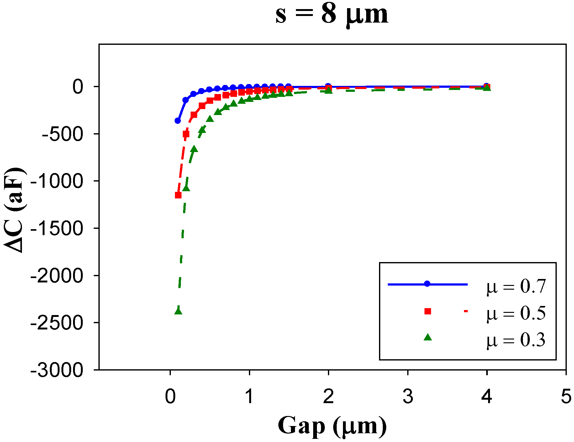
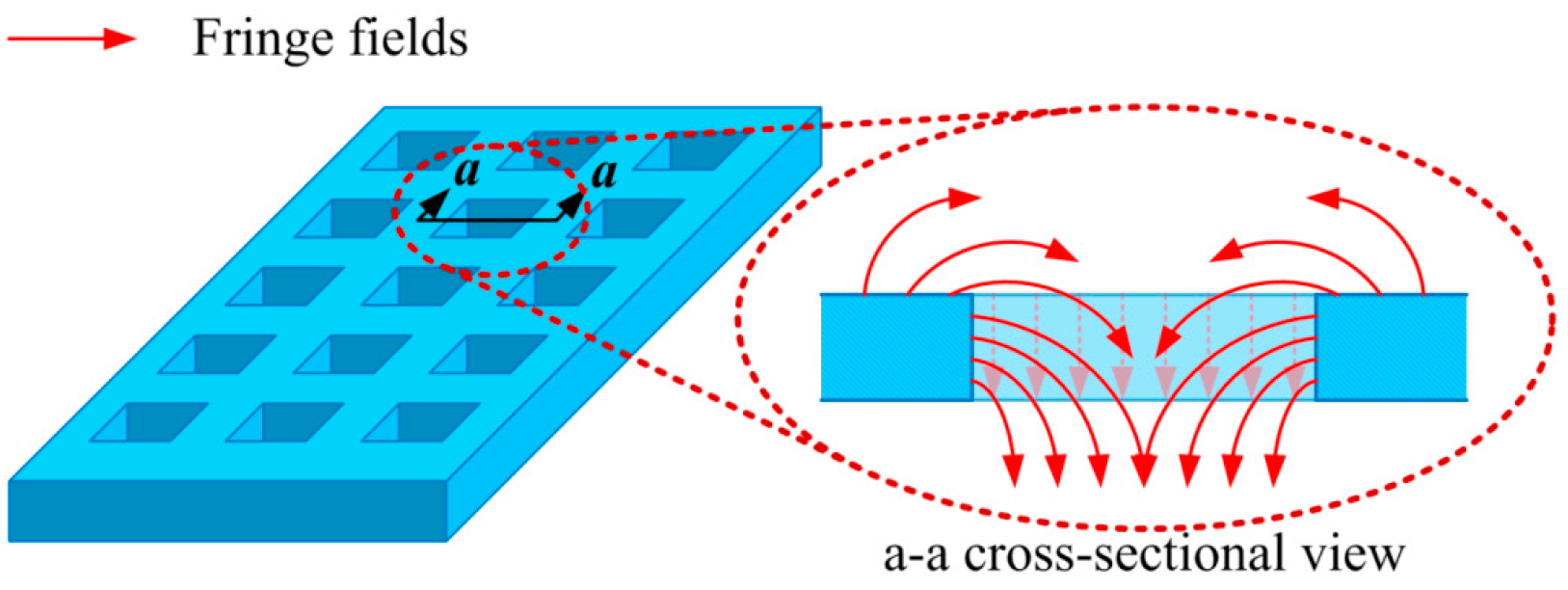
We make perforated micro-beams to demonstrate the application of the present capacitance compensation formula on determine their capacitance.
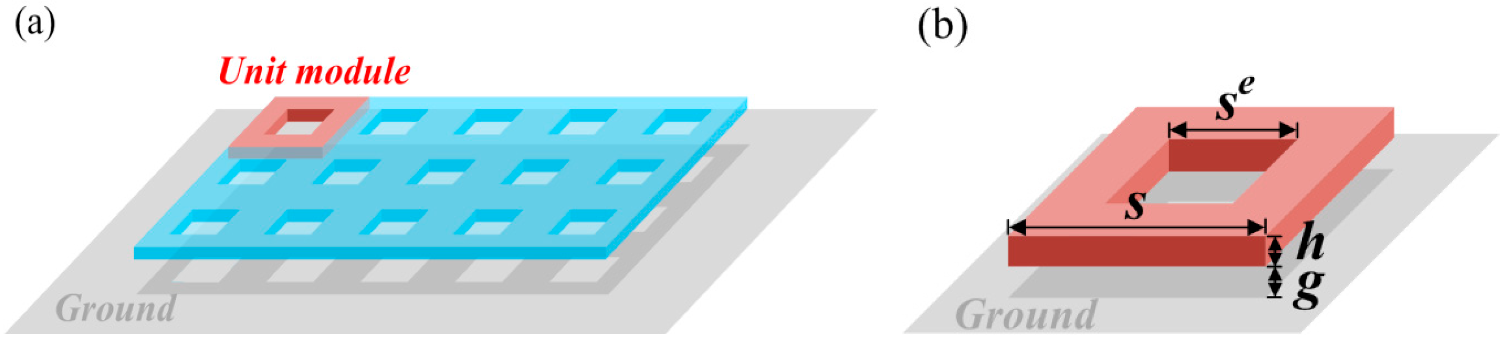
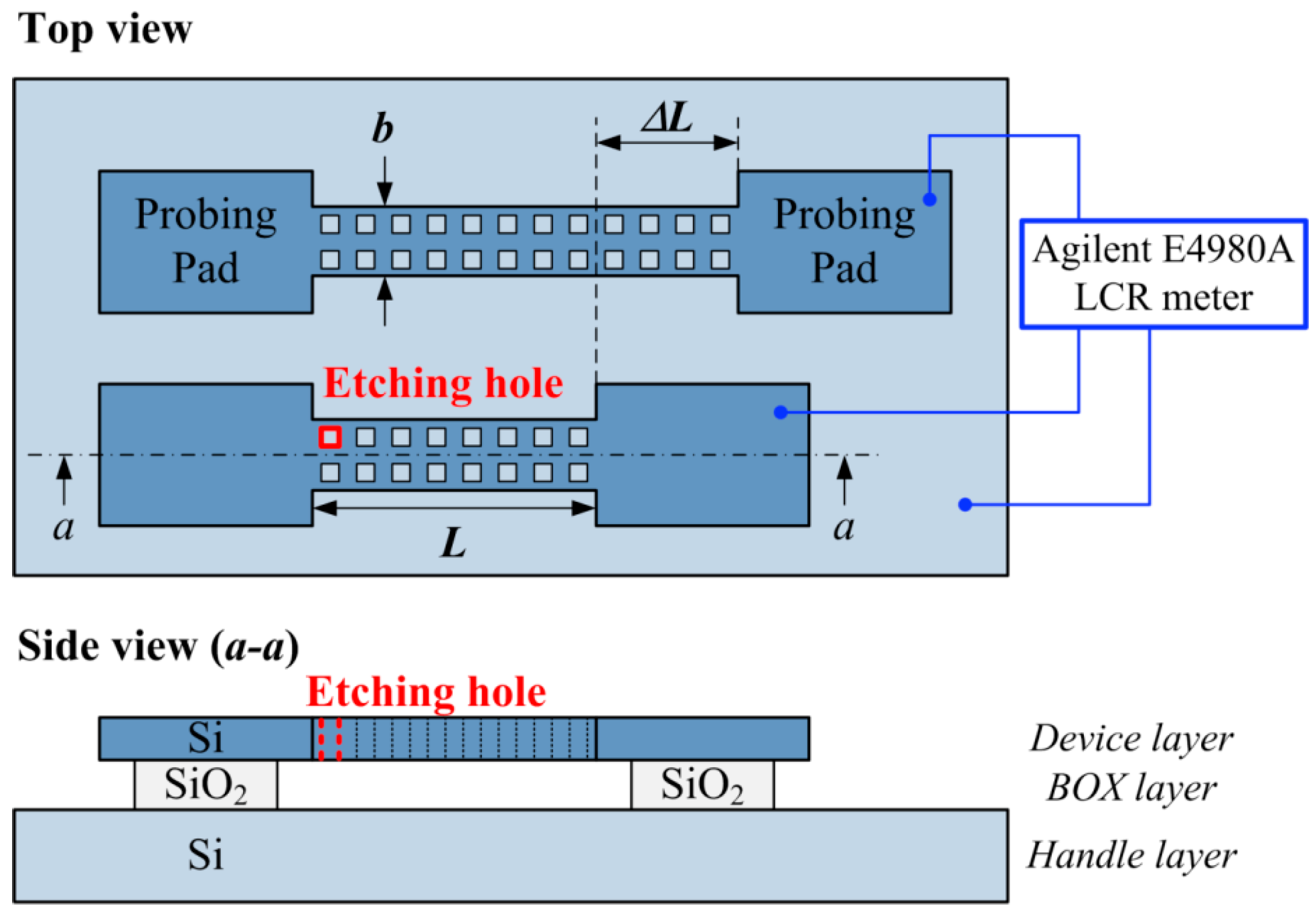
Figure 10 shows the schematic of the test micro-beam. A series of micro-beams with different lengths, widths, and etching-hole sizes are manufactured by the MEMS process.
Table 5 lists the dimensions of the test micro-beams. In total, there are nine test-chips containing 54 test-beams. By unit-module length, they are divided into three groups. Each group contains three chips and the three chips have three different ligament coefficients (μ). Each chip contains six beams (
Figure 11). By width, they are divided into two groups; each group contains three beams with three different lengths.
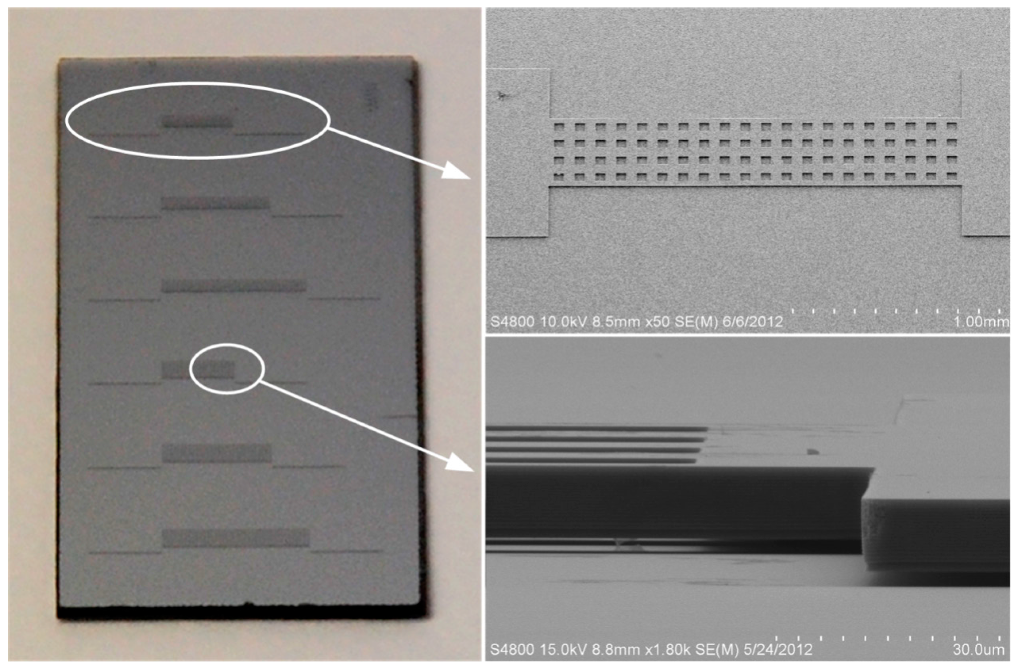
To control the size of the test structure precisely, the authors adopt a low-resistance silicon-on-insulator (SOI) wafer to make the micro-beam.
Table 6 details the specifications of the SOI wafer. The device layer forms the beam structure (thickness = 10 μm), which is patterned by induction coupling plasma etching. The buried oxide layer forms the anchor of the test structure and decides the gap between micro-beam and substrate (gap = 2 μm). After patterning the device layer, 49% Hydrogen Fluoride etchant is used to etch the silicon dioxide under the device layer and makes the micro-beam release. The scanning electron microscope picture (
Figure 11) shows that the test beam with etching holes is completely suspended and without curl.
Figure 10.
The schematic of test microstructures. L: length of the test beam.
Figure 11.
The scanning electron microscope picture of the test sample.
The capacitances of the test structures are measured by Agilent E4980A LCR meter (Agilent Technologies, Santa Clara, CA, USA) (
Figure 10). To eliminate the fringe effects of the probing pads and anchors, two test beams with different lengths fabricated in the same chip are required. The capacitance difference (
CΔL) of the two beams is obtained by mutually subtract their capacitances measured by Agilent E4980A LCR meter. The experiment results are listed in the sixth column of
Table 7,
Table 8 and
Table 9. The authors of this paper had published a two-dimensional capacitance formula for determining the capacitance of the micro-beam without etching hole [
11], we can use that formula to calculate the capacitance difference of the present two test beams, that is:
where
is the length difference of the two test beams. It should be mentioned here that Equation (8) does not consider the effects of etching holes. The results of Equation (8) are listed in the 6th column of
Table 7,
Table 8 and
Table 9. For considering the effects of etching holes, we can add Equation (7) into Equation (8) to calculate the capacitance difference of the present two test beams, that is:
where Δ
C is given by Equation (7) and
N is the total number of etching holes. The results of Equation (9) are listed in the ninth column of
Table 7,
Table 8 and
Table 9.
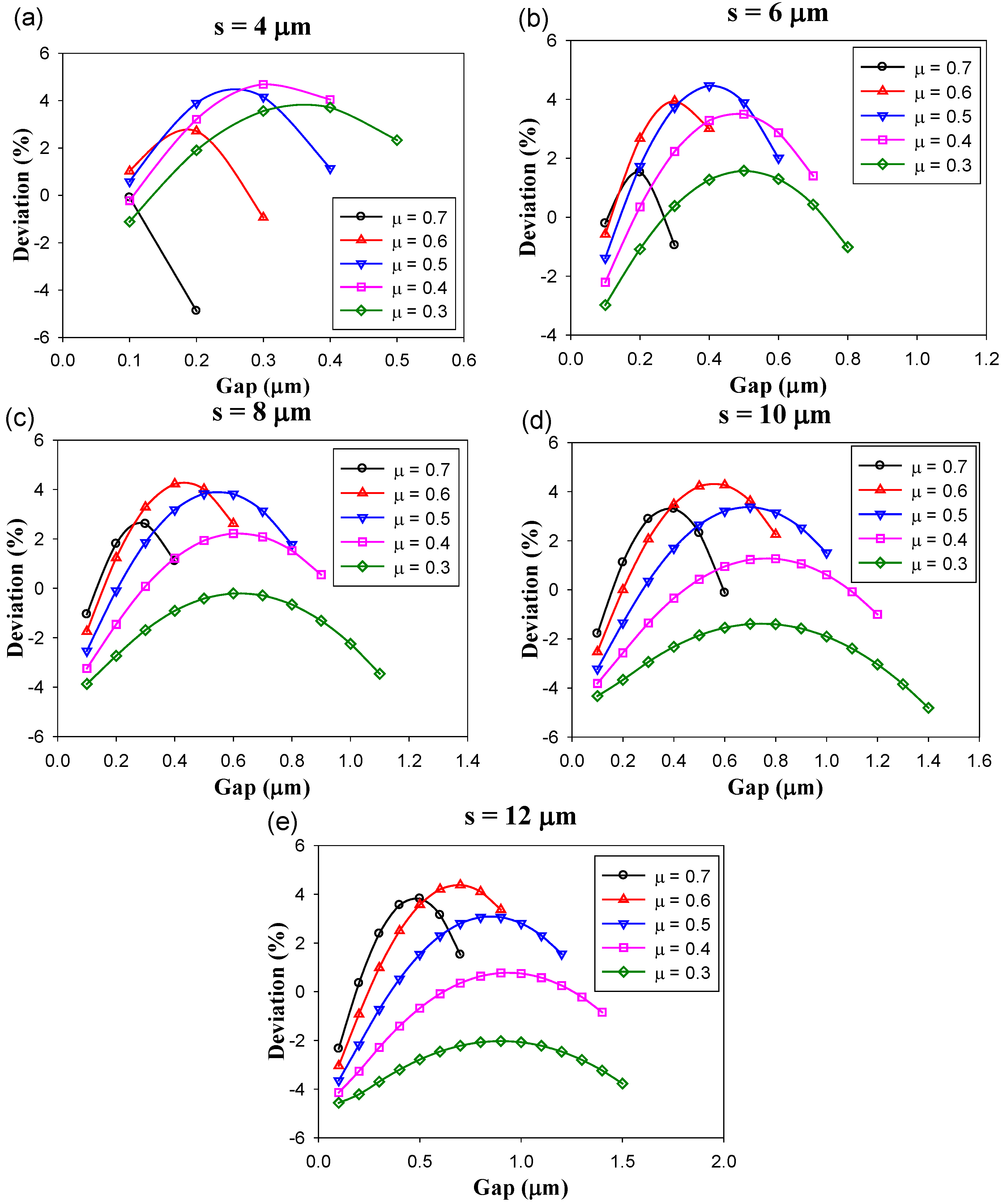
Table 7,
Table 8 and
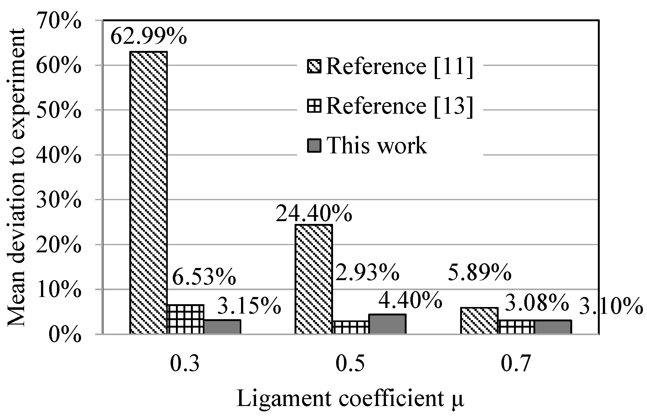
Table 9 compare the numerical results obtained by experiment and empirical formula for the ligament coefficients μ = 0.7, 0.5 and 0.3, respectively. The smaller the ligament coefficient is, the larger the total area of the etching holes is. When the ligament coefficient μ is 0.7 (
Table 7), the mean deviation between Equation (8) (neglecting the effect of etching hole) and experiment is 5.89%, while those of this work and the authors’ previous work [
13] are both about 3%. When the ligament coefficient μ is 0.5 (
Table 8), the mean deviation of Equation (8) reaches to 24.40%, while those of this work and the authors’ previous work [
13] are about 4% and 3% respectively. When the ligament coefficient μ = 0.3 (
Table 9), the most critical case in experiment and regular design, the deviation of Equation (8) reaches to 62.99%, while those of this work and the authors’ previous work [
13] are about 3% and 7%, respectively. This is because the larger etching holes cause a significant capacitance decrease, but Equation (8) neglects the effect of etching hole.
Figure 12 summarizes
Table 7,
Table 8 and
Table 9. According to the aforementioned results and comparisons, accompanied with the capacitance compensation term of this work, Equation (7), significantly improves the capacitance prediction of the microstructures with etching holes. The maximum deviation of the 54 test-beams compared with experiment is within 8%. The present capacitance compensation term of etching holes can provide the MEMS designers to estimate the capacitance of micro-devices with etching holes and predominate in the device characteristics.
Figure 12.
Comparisons of capacitance between experiment and formulae, summary of
Table 6,
Table 7 and
Table 8.


