Article

Multifunctional Material Structures Based on Laser-Etched Carbon Nanotube Arrays

Information and Communications Technologies, Electronics and Applied Mathematics (ICTEAM), Université Catholique de Louvain, 1348 Louvain-la-Neuve, Belgium
*
Author to whom correspondence should be addressed.
Micromachines 2014, 5(3), 756-765; https://doi.org/10.3390/mi5030756
Submission received: 1 August 2014 / Revised: 10 September 2014 / Accepted: 12 September 2014 / Published: 22 September 2014
(This article belongs to the Special Issue Laser Micro- and Nano- Processing)

Abstract

:
High-power electronics in the transportation and aerospace sectors need size and weight reduction. Multifunctional and multistructured materials are currently being developed to couple electromagnetic (EM) and thermal properties, i.e., shielding against electromagnetic impulsions, and thermal management across the thermal interface material (TIM). In this work, we investigate laser-machined patterned carbon nanotube (CNT) micro-brushes as an alternative to metallic structures for driving simultaneously EM and heat propagation. The thermal and electromagnetic response of the CNT array is expected to be sensitive to the micro-structured pattern etched in the CNT brush.

Graphical Abstract

1. Introduction

Multifunctional materials are expected to solve the challenge of size and weight reduction of on-board electronic hardware designed for railway, airborne, and space technologies: thermal interface materials or filled materials are used to manage the thermal heat hotspot dissipations and electromagnetic (EM) absorbers are aiming to protect devices against EM radiation from neighboring communication systems. Various periodic structures such as arrays of metallic wires, have been developed for more than 10 years for EM applications from 100 MHz up to THz and optical range [1,2]. They belong to a particular class of metamaterials, aiming at driving EM propagation in some unconventional ways. Carbon nanotube (CNT) dispersed in composites are already known as broadband microwave absorbers [3,4]. The absorption depends on the CNT orientation inside the polymer matrix of the composite [5]. Pure CNT squared arrays of vertical metal wires offer new solutions to tailor EM absorption in specific directions and frequency ranges, allowing control of the propagation of thermal and EM wavefronts along particular spatial directions. They are also expected to have a high and spatially anisotropic thermal conductivity (along the CNT axis). The higher vertical aligned CNT arrays’ thermal conductivity is around 265 W/m K [6]. These CNT array structures are currently investigated as an alternative to cooling systems using circulation of fluids to drive dissipated thermal power outside a system. Also, periodic patterns of CNT can offer interesting potential in the field of photovoltaics and energy harvesting in the THz range [7]. Characteristic dimensions of the pattern can be adjusted in order to perfectly absorb the power around a given THz frequency, making the structure able to reemit at the same frequency, and act as a selective thermal emitter with enhanced control of the emissivity.
In this paper, we present the laser-etching post-process optimization used to obtain adequate micro-structured CNT brushes for such coupled EM/thermal application, assessed by some preliminary electromagnetic and thermal characterizations. The supported CNT brush is micro-patterned using a picosecond laser-etching system (model Oxford J-1064/355, Oxon, UK) to etch different patterns into the CNT brush: parallel trenches 50 or 100 μm wide, and 50 µm or 100 µm nano-pillars separated by 50 µm.

2. Experimental Section

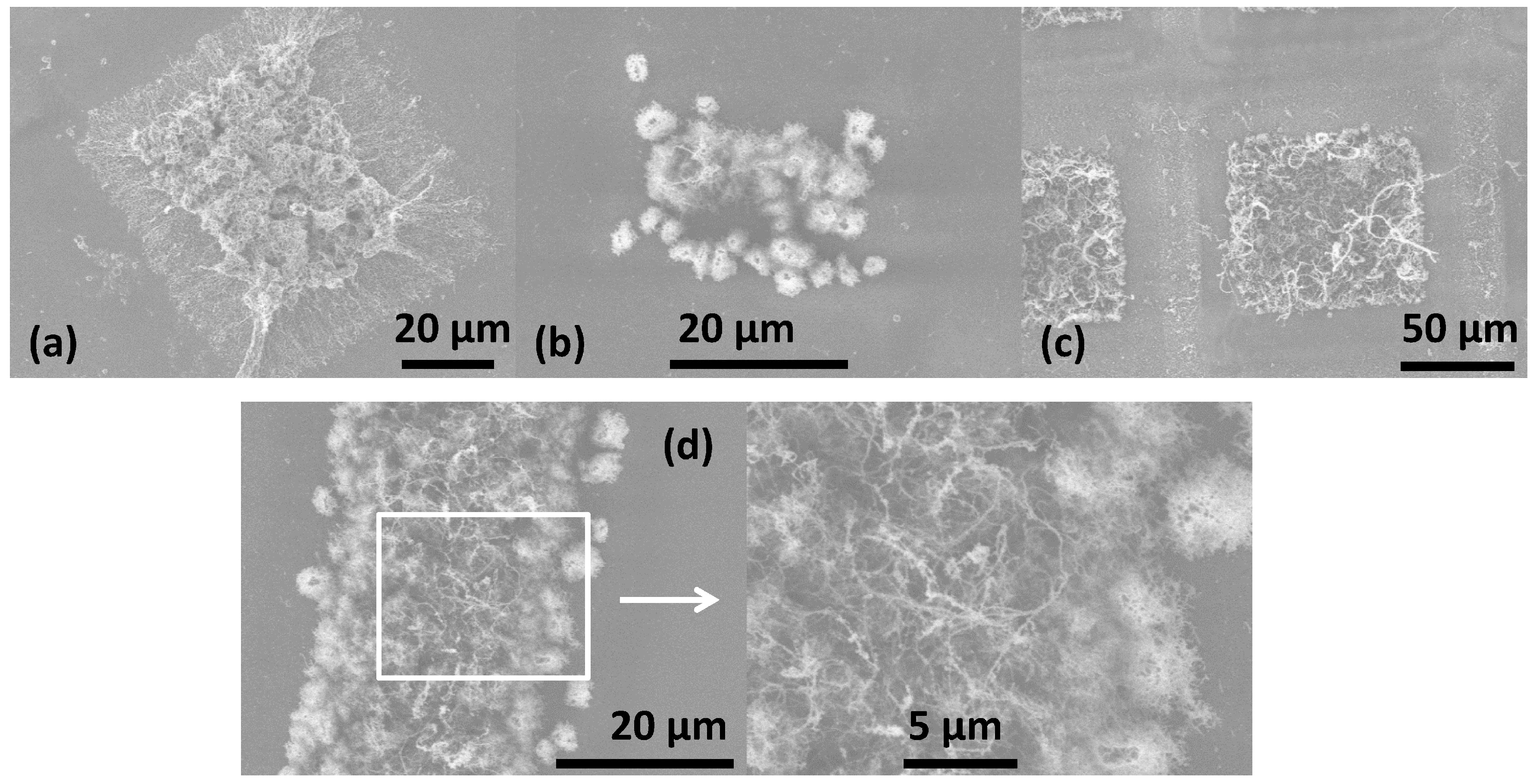
2.1. CNT Brush Processing

The samples of multiwall CNT brushes are provided by Nanocyl SA Company (Sambreville, Belgium). They are fabricated using the growing of CNT with average length of 50 µm (with an average diameter of 50 nm) on a quartz (SiO2) substrate with a surface of 5 mm2 via the catalytic chemical vapor deposition (CVD) method. Figure 1 provides a scanning electron micrography (SEM) showing the area where the CNT brush has grown (left) and the bulk quartz-supporting substrate (right).
Figure 1. Scanning electron micrography (SEM) images of the supported carbon nanotube (CNT) after growing (left area: CNT; right area: quartz substrate) [8].
Micromachines 05 00756 g001
The pattern repeatability and accuracy of the laser-etching post-process can be controlled through the etching parameters and is dependent on the quality of the CNT brush-growing process (flatness/rugosity of the quartz substrate and adhesion strength of the CNT onto its surface). The resulting pattern is observed to be reproducible. The wavelength of the laser pulse is 355 nm. The spot diameter in the focal plane is close to 10 μm.

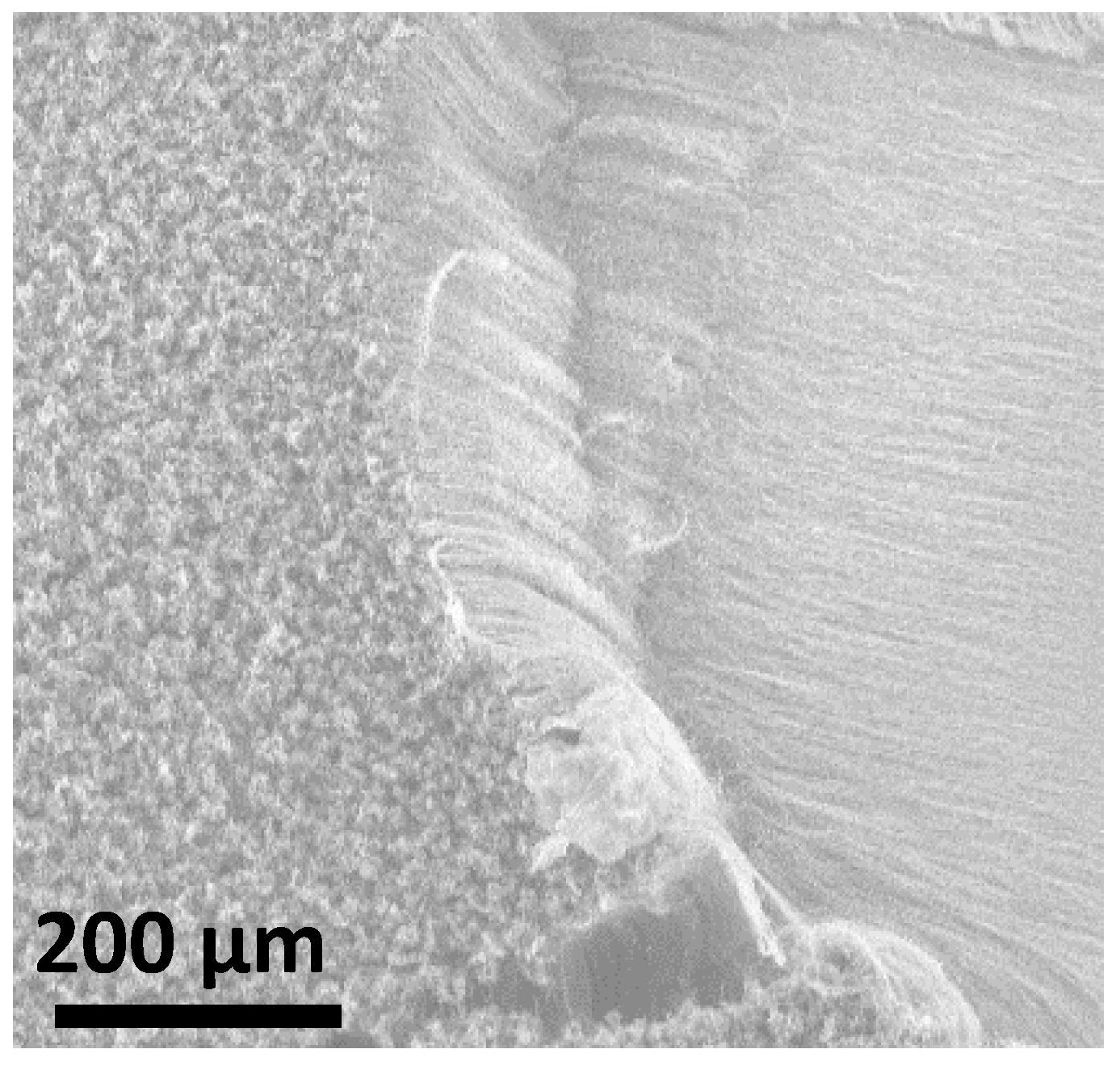
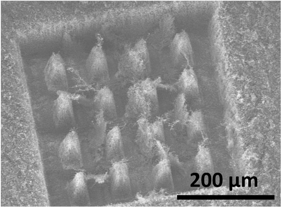
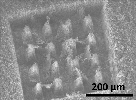
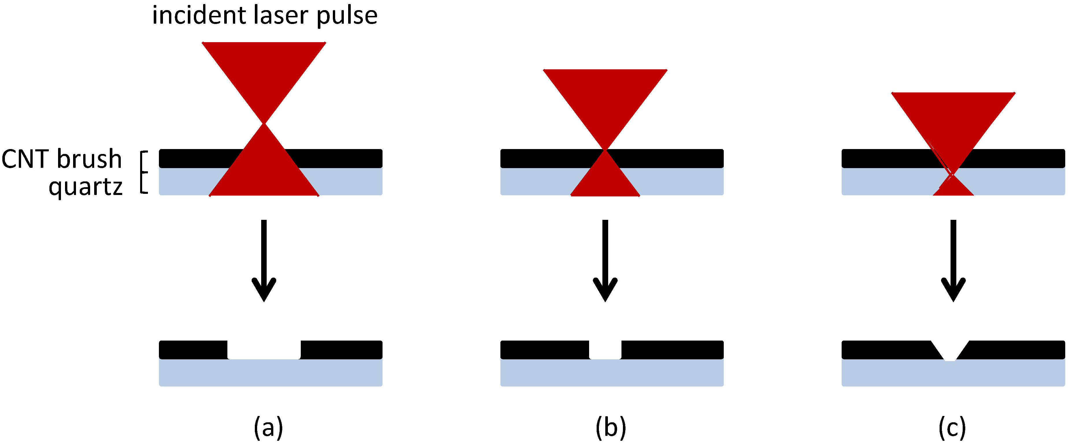
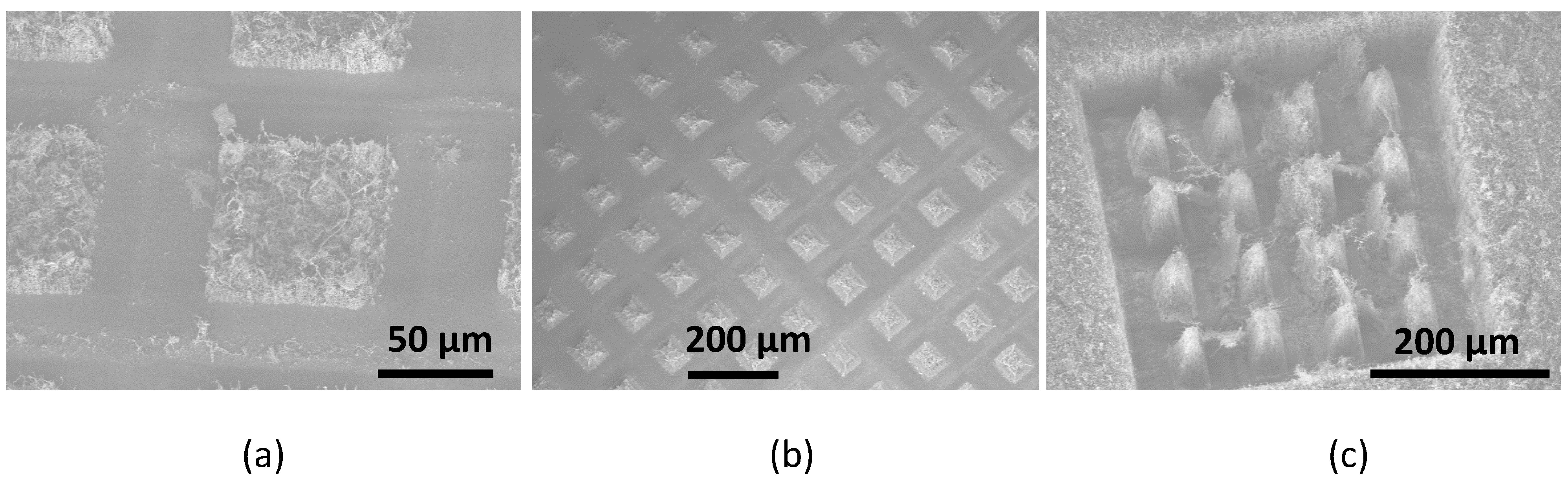
2.2. Laser Processing

The interaction between the laser pulse and the sample determines the resulting etch resolution. The different parameters are the scan rate and the pulse frequency, the scan repetition, the laser average power, and the focus offset during the etching post-processing (i.e., with an offset of 400 μm, the spot diameter resolution is 20 μm). Figure 2 and Figure 3 show the impact of an offset focus on the resulting pattern: if the focus point is above the substrate (Figure 2a,b), the etched edges are well defined and vertical as observed in Figure 3a; while the pyramid structure is observed for an inside surface focus point (Figure 2c and Figure 3b,c). All the parameters used for the laser processing of structures in Figure 3 and Figure 4 are reportedin Table 1.
Figure 2. Schematic view of the interaction between the laser spotlight and the sample during the etching post-process: (a) When the focus point is above the sample surface; (b) when the focus point is on the substrate; and (c) when the focus point is on the substrate surface or inside the substrate.
Micromachines 05 00756 g002
Table 1. Laser parameters used for the etching step.
PatternSpot size expected (µm × µm)Average power (mW)Offset focus (µm)Scan repetitionsScan rate (mm/s)Pulse frequency (kHz)
Pattern 1100 × 10014601550100
Pattern 2100 × 100310Positive1550100
Pattern 3100 × 1003107001550100
Pattern 450 × 503107001550100
Pattern 5100 × 100146Positive1550100
Pattern 6100 (microline)3107001550100
Figure 3. SEM images of the CNT vertical array structure after the etching post-processwith the following parameters, with 100 µm × 100 µm plot size expected: (a) Pattern 1, (b) Pattern 2 and (c) Pattern 3.
Micromachines 05 00756 g003
Figure 4a–c show the SEM images of different etched CNT micro-pillars with a 100 µm × 100 µm expected size. Depending on the effective average power used, the pattern quality is highly modified. The darker zone in SEM images is the substrate. Some CNT are “burned” during the etch post-process on the sample (for 310 mW average laser power), as observed in Figure 4a,b. This results in quite unformed micro-pillars or pillars with deformed CNT, as also observed in Figure 4a,b. In Figure 4d, the expected micro-line length is 100 µm. Partial burn is observed. Reducing the average power allows for a well-defined structure as shown in Figure 4c, with intact CNT.
Figure 4. SEM images of the CNT micro-pillars and a micro-line: (a) Pattern 2, (b) Pattern 4, (c) Pattern 5 and (d) Pattern 6.
Micromachines 05 00756 g004
The quality and the resolution of the pattern depend on the height of the CNT and limitations of our laser process. The height of the CNT array is fixed by the CVD process parameters. The power must be decreased when the CNT length is less than 50 µm in order to preserve the CNT structure. In the focus plane, the lowest etched surface has a diameter of 10 µm, and the final structures can have a minimal resolution of 10 µm, with a minimal period of 50 µm.
The CNT pattern can be obtained by other techniques. The table below compares three techniques (Table 2): selective chemical vapor deposition (CVD) [9], laser micromachining or dry micro-electro-discharge machining [10,11,12].
Table 2. Comparison of methods for patterning of CNT arrays.
Parameters for comparisonSelective CVD processLaser patterningDry micro-electro-discharge
“Etched” surface resolutionDepends on the pre-patterned catalyst resolution on the substrate10 µm
(15 µm from [1] with a focus offset of ~800 µm)
Dependent on the electrode diameter and the discharge gap clearance
  • Normal polarity: 93 µm and 7.5 µm (total: 108 µm) from [10]; or 64 µm and 24 µm (total:112 µm) from [11]
  • Reverse polarity: 93 µm and 2.5 µm (total: 98 µm) from [10]; or 64 µm and 7 µm (total: 78 µm) from [11]
Maximum surfaceSeveral cm2Several cm2Several mm2 from [10,11] (dependent on the number of electrodes [12])
CNT length limitation and the pattern resolution
  • depends on the ratio between the length of the CNT and the period of the pattern (because the CNT in an array can bend under their own weight [9])
  • depends on the CNT array density and the CNT diameter (and type)
Debris left after processNo debrisLess debris for the optimal average power (if too low: some etched CNT stay on the substrate in the etched areas; if too high: damage to the substrate)Less debris with the reverse polarity [10,11]
ThroughputNot applicableA few minutes for 5 mm2A few minutes for 5 mm2
AmbientNot applicableProcess in ambient airAmbient air (from [10])
N2–O2 or SF6–O2 (from [11])
ConstraintsKnowledge of the pattern before the processThe parameters depend on the CNT density and the brush heightHigh dependence on the electrode dimension
The best quality of the pattern is obtained by the selective CVD process [9] but this implies fixing the pattern prior to the growing of the CNT brush, and requires a good knowledge of the CVD process. Contrarily, the laser patterning [1] or the dry micro-electro-discharge patterning [10,11,12] can be used as post-process, depending on the desired pattern that can be adjusted/modified at will.

3. Results and Discussion

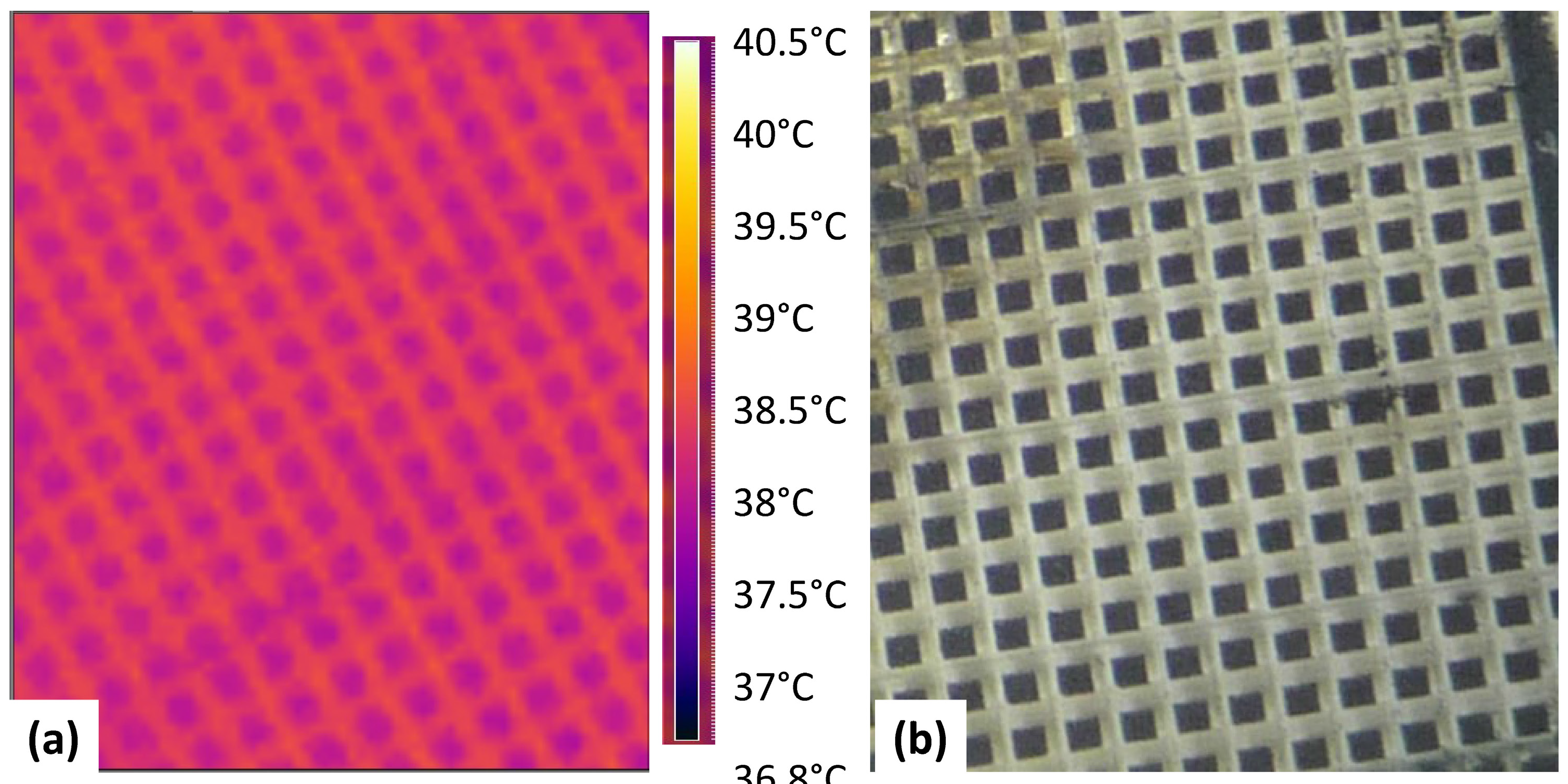
3.1. Thermal Preliminary Measurements

The thermography measurement setup consists in an NIR camera (model FLIR SC660, Meer, Belgium), and a thermal source (a thermal resistance in this case). The first thermal measurements were done to observe the difference of emissivity between the quartz and the etched pattern at constant temperature (Figure 5). This allows us to obtain a reference measurement first in order to characterize in detail the anisotropic thermal diffusivity, thermal conductivity and EM properties of the material in the THz range of frequency.
Figure 5. View of a pattern with 50 µm × 50 µm CNT array nano-pillars grown on a quartz substrate: (a) Infrared thermography with a resolution size of 25 µm × 25 µm per pixel on a constant temperature polyimide source (30 °C). (b) Optical microscope image.
Micromachines 05 00756 g005
The emissivity (εtape) of a tape sample taken as reference is 0.95. From the equation
ε s a m p l e = ( T s a m p l e T e n v i r o n m e n t T t a p e T e n v i r o n m e n t ) × ε t a p e
with Tsample, Tenvironement, and Ttape, respectively, being the sample, laboratory room, and tape temperatures. The calculated emissivities (εsample) are 0.9 for the CNT micro-pillars and 0.96 for the quartz in the 9–14 µm wavelength.

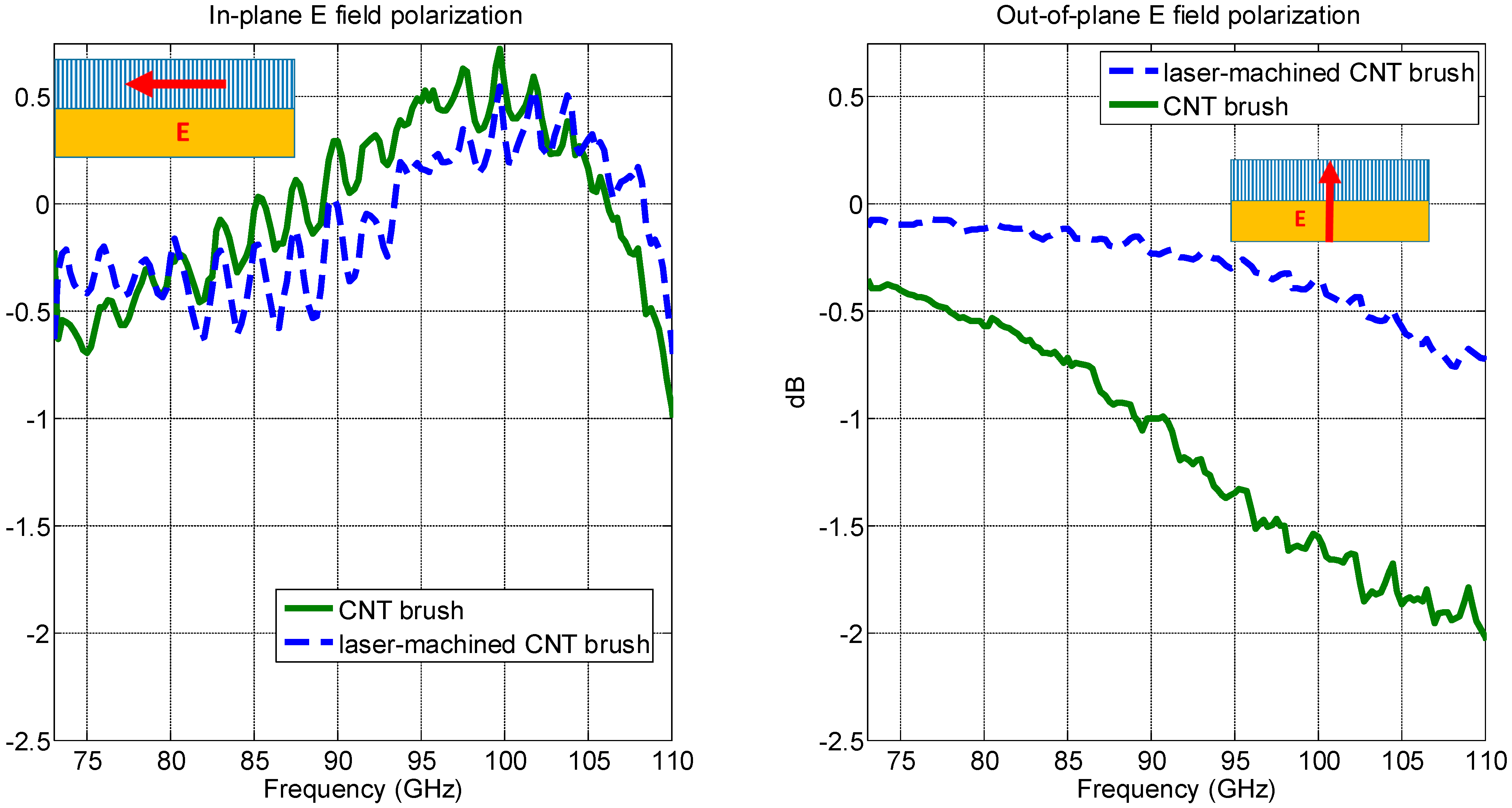
3.2. EM Characterization

Figure 6 shows an EM characterization performed in the sub-THz range (up to 110 GHz) in order to investigate the sensitivity of the EM polarization to the spatial anisotropy of the CNT brush, implying anisotropic electrical conductivity of the equivalent effective medium. The transmission of the EM wave through the CNT brush samples (patterned by laser micro-machining or otherwise) is measured for two different polarizations of the electric field, and normalized to the measurement for the same polarization made on a quartz sample without CNT brush. When the incident electric field E is parallel to the axis of the CNT (out-of-plane polarization, meaning E field normal to the plane of the quartz substrate), a significant attenuation of the signal is observed, being more pronounced when the brush is not patterned, in accordance with the higher density of CNT covering the sample in this latter case. When the E field is in the plane of the sample (i.e., perpendicular to the CNT main axis) normalized attenuation becomes insignificant (within ±0.5 dB), in accordance with the fact that no interaction occurs between the elongated conductive nanotubes and the incident electric field.
Figure 6. Measurement of transmission for incident E field polarization shown in the inset, without (solid) or with (dashed) laser-patterning of the CNT brush (100 µm square micro-pillars spaced by 50 µm, 5 mm square). Measurements are normalized to the transmission measured for a quartz sample without CNT brush.
Micromachines 05 00756 g006
Further analysis of the effect of patterning at higher frequency is under progress. Figure 7 shows a prediction of resonance absorption in the THz range, following the approach adapted from [13] for patterns of nanowires. The 50 µm × 50 µm squared CNT plot has a spatial anisotropy of its macroscopic permittivity expressed as:
ε x = ε y = ( 1 + p ) ε C N T + 1 p ( 1 p ) ε C N T + 1 + p  
ε z = p   ε C N T + 1 p
where the z-axis is along the main axis of the nanotubes (i.e., normal to the plane of the quartz), p is the volumetric fraction of CNTs in the brush and εCNT is the permittivity of a single CNT, a function of its axial conductivity σCNT:
ε C N T = 1 + σ C N T j ω ε o
The equivalent volumetric conductivity of a single nanowire follows a Drude-like formalism as proposed in [14]
σ C N T = 8 e 2 v F h ( j ω + 1 τ ) π r 2
with e being the electron charge, vF the Fermi velocity in the CNT (= 9.76 × 10⁵ m/s), h the Planck constant, τ the relaxation time (=3 × 10⁻¹² s) and r the radius of the nanotube.
Figure 7 shows that the CNT plot is able to focus/trap the electric field at dedicated THz frequencies, with resulting enhanced absorption induced by the conductivity of the CNT. Also the position and number of resonances over a given frequency range depend on the number of plots in the array, indicating that the resonances and resulting absorption windows can be tuned by the size and periodicity of the array, in accordance with resonance splits resulting from coupling between resonators.
Figure 7. (Left) absorption for a single CNT plot (top) and electric field pattern at frequency 1.332 THz, (Right) absorption for a 3 × 3 array of CNT plots (top) and electric field pattern at frequency 1.284 GHz.
Micromachines 05 00756 g007

4. Conclusions

We are able to control the parameters to obtain the desired patterns by a laser-etching post-process. First thermal measurements were taken to observe the emissivities for constant temperature of measurement. Further measurements and simulations are in progress to obtain the thermal diffusivity, conductivity, and EM properties of the material in the GHz and THz range of frequency. According to the needs of space, railway, aeronautic and other applications requiring energy harvesting, the CNT arrays will be included inside multilayer structures and the properties will be measured up to the THz range.

Acknowledgments

The authors are grateful to the National Fund for Scientific Research (F.R.S.-FNRS) and the ATAC-Concept project for funding this research. The help of Pascal Simon, Mathieu Vanden Bulcke, David Spôte and Daniel Bonduel for providing access to process and characterization facilities are sincerely acknowledged. We thank Professors Christian Bailly and Thomas Pardoen for fruitful discussions. This work is also supported by the MINATIS project co-funded by the European Regional Development Fund (ERDF) and the Walloon region.

Author Contributions

The authors contributed equally to this research.

Conflicts of Interest

The authors declare no conflict of interest.

References

  1. Kordás, K.; Tóth, G.; Moilanen, P.; Kumpumäki, M.; Vähäkangas, J.; Uusimäki, A.; Vajtai, R.; Ajayan, P.M. Chip cooling with integrated carbon nanotube microfin architectures. Appl. Phys. Lett. 2007, 90, 123105. [Google Scholar]
  2. Qi, Z. Electromagnetic radiation of carbon nanotube array in microwave frequencies. In Proceedings of Asia-Pacific Microwave Conference, Yokohama, Japan, 12–15 December 2006; pp. 701–703.
  3. Huynen, I.; Quiévy, N.; Bailly, C.; Bollen, P.; Detrembleur, C.; Eggermont, S.; Molenberg, I.; Thomassin, J.M.; Urbanczyk, L.; Pardoen, T. Multifunctional hybrids for electromagnetic absorption. Acta Mater. 2011, 59, 3255–3266. [Google Scholar] [CrossRef]
  4. Emplit, A.; Tao, F.; Bailly, C.; Huynen, I. Novel family of broadband nanocomposite microwave absorbers with carbon nanotubes in solid polymer film. In Proceedings of European Microwave Conference, Nuremberg, Germany, 6–10 October 2013; pp. 778–781.
  5. Marconnet, A.M.; Yamamoto, N.; Panzer, M.A.; Wardle, B.L.; Goodson, K.E. Thermal conduction in aligned carbon nanotube-polymer nanocomposites with high packing density. ACS Nano 2011, 5, 4818–4825. [Google Scholar] [CrossRef] [PubMed]
  6. Tong, T.; Zhao, Y.; Delzeit, L.; Kashani, A.; Meyyappan, M.; Majumdar, A. Dense vertically aligned multiwalled carbon nanotube arrays as thermal interface materials. IEEE Trans. Compon. Packag. Manuf. Technol. 2007, 30, 92–100. [Google Scholar]
  7. Liu, X.; Tyler, T.; Starr, T.; Starr, A.F.; Jokerst, N.M.; Padilla, W.J. Taming the blackbody with infrared metamaterials as selective thermal emitters. Phys. Rev. Lett. 2011, 107, 045901. [Google Scholar] [CrossRef]
  8. Emplit, A.; Huynen, I. Carbon nanotubes arrays for coupled electromagnetic and thermal management in high power electronics: influence of microstructuration and stress investigated by IR thermography. In Proceedings of the Fourteenth Intersociety Conference on Thermal and Thermomechanical Phenomena in Electronic Systems, Orlando, FL, USA, 27 May–30 June 2014; pp. 1379–1384.
  9. Brun, C.; Franck, P.; Chow, W.L.; Coquet, P.; Baillargeat, D.; Tay, B.K. Horizontal and vertical carbon-nanotube-array-based antenna design. In Proceedings of European Microwave Conference, Nuremberg, Germany, 6–10 October 2013; pp. 377–380.
  10. Saleh, T.; Dahmardeh, M.; Bsoul, A.; Nojeh, A.; Takahata, K. High-precision dry micro-electro-discharge machining of carbon-nanotube forests with ultralow discharge energy. In Proceedings of IEEE 25th International Conference on Micro Electro Mechanical Systems (MEMS), Paris, France, 29 January–2 February 2012; pp. 259–262.
  11. Saleh, T.; Dahmardeh, M.; Nojeh, A.; Takahata, K. Dry micro-electro-discharge machining of carbon-nanotube forests using sulphur-hexafluoride. Carbon 2013, 52, 288–295. [Google Scholar]
  12. Sarwar, M.S.U.; Dahmardeh, M.; Nojeh, A.; Takahata, K. Batch-mode micropatterning of carbon nanotube forests using UV-LIGA assisted micro-electro-discharge machining. J. Mater. Process. Technol. 2014, 214, 2537–2544. [Google Scholar]
  13. He, Y.; Deng, H.; Jiao, X.; He, S.; Gao, J.; Yang, X. Infrared perfect absorber based on nanowire metamaterial cavities. Opt. Lett. 2013, 38, 1179–1181. [Google Scholar] [CrossRef] [PubMed]
  14. Franck, P.; Baillargeat, D.; Tay, B.K. Mesoscopic model for the electromagnetic properties of arrays of nanotubes and nanowires: A bulk equivalent approach. IEEE Trans. Nanotechnol. 2012, 11, 964–974. [Google Scholar] [CrossRef]

