Fabrication and Characterization of Flexible Electrowetting on Dielectrics (EWOD) Microlens

Abstract
:1. Introduction
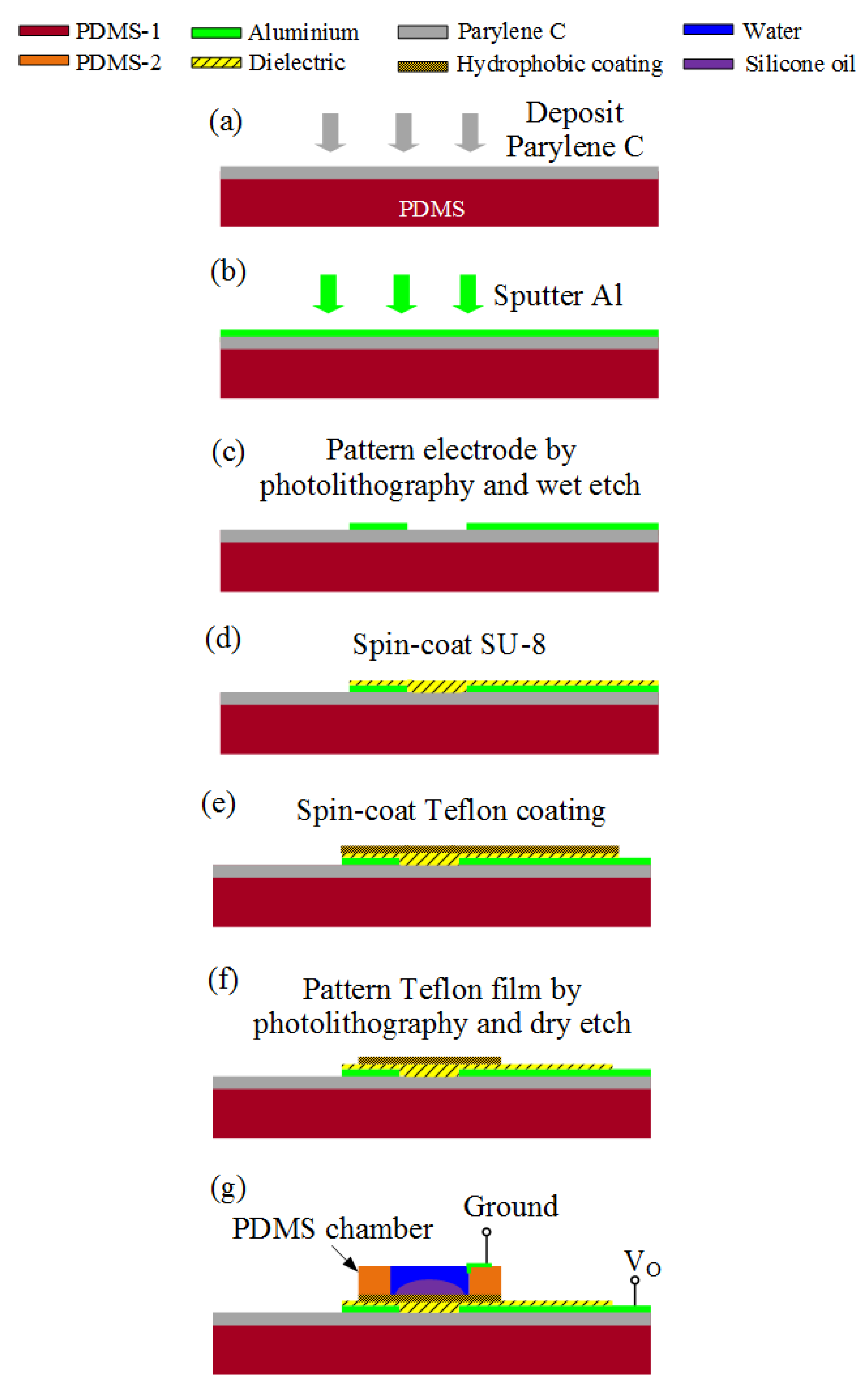
2. Mechanism and Fabrication
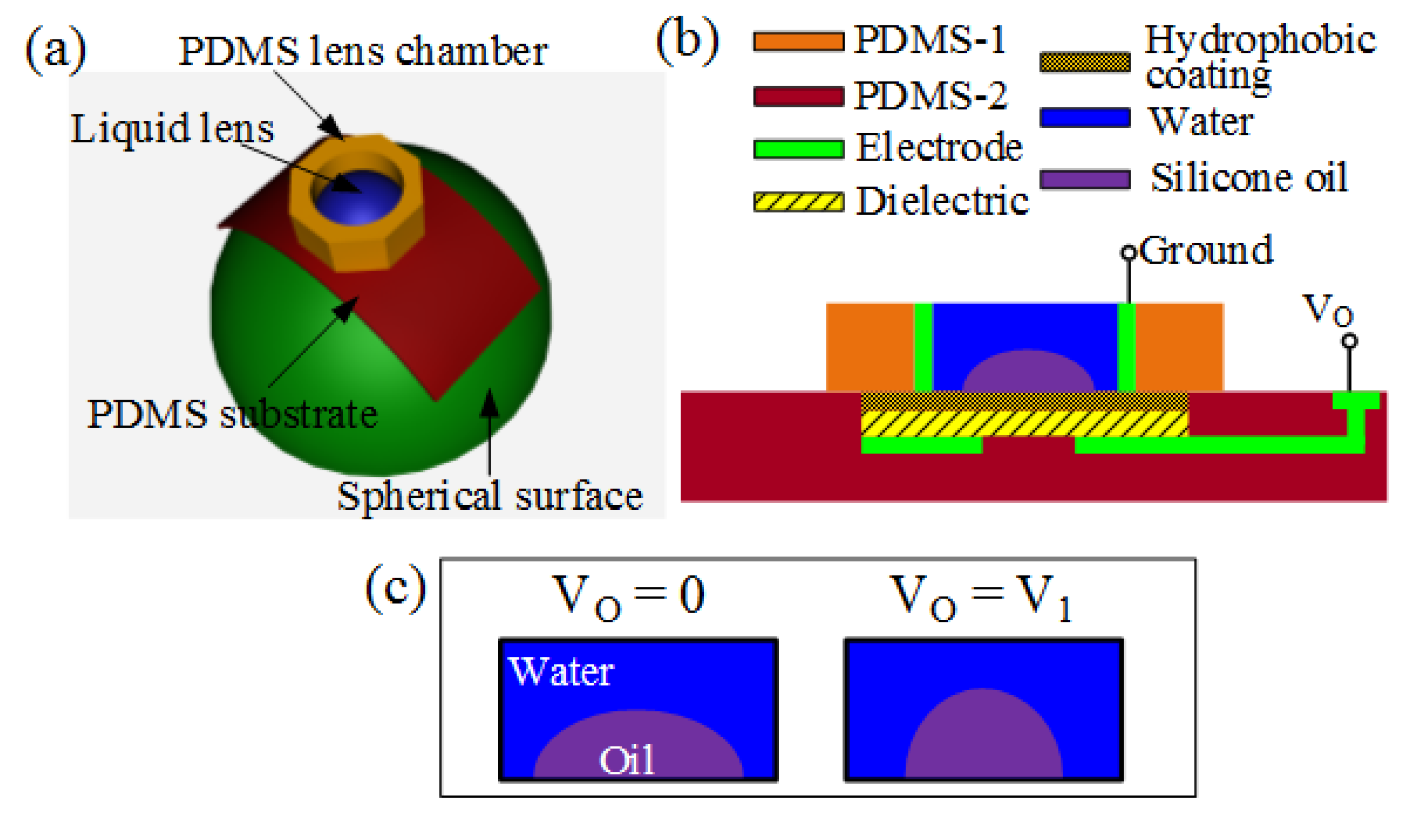
2.1. Mechanism


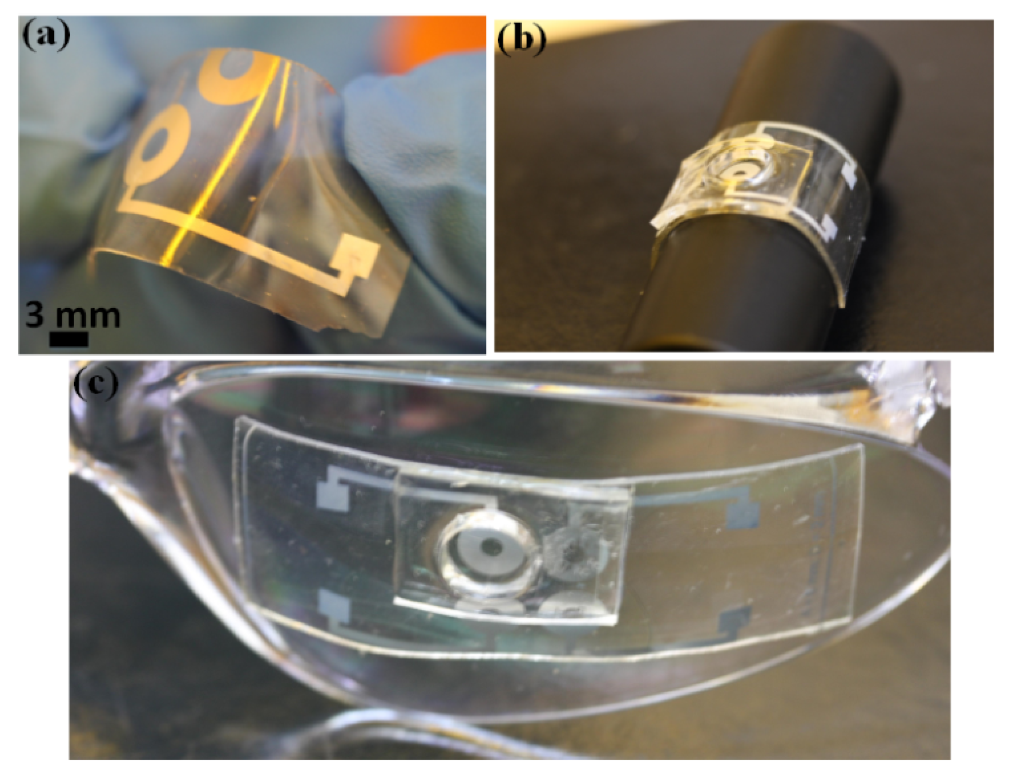
2.2. Fabrication

3. Results and Discussion
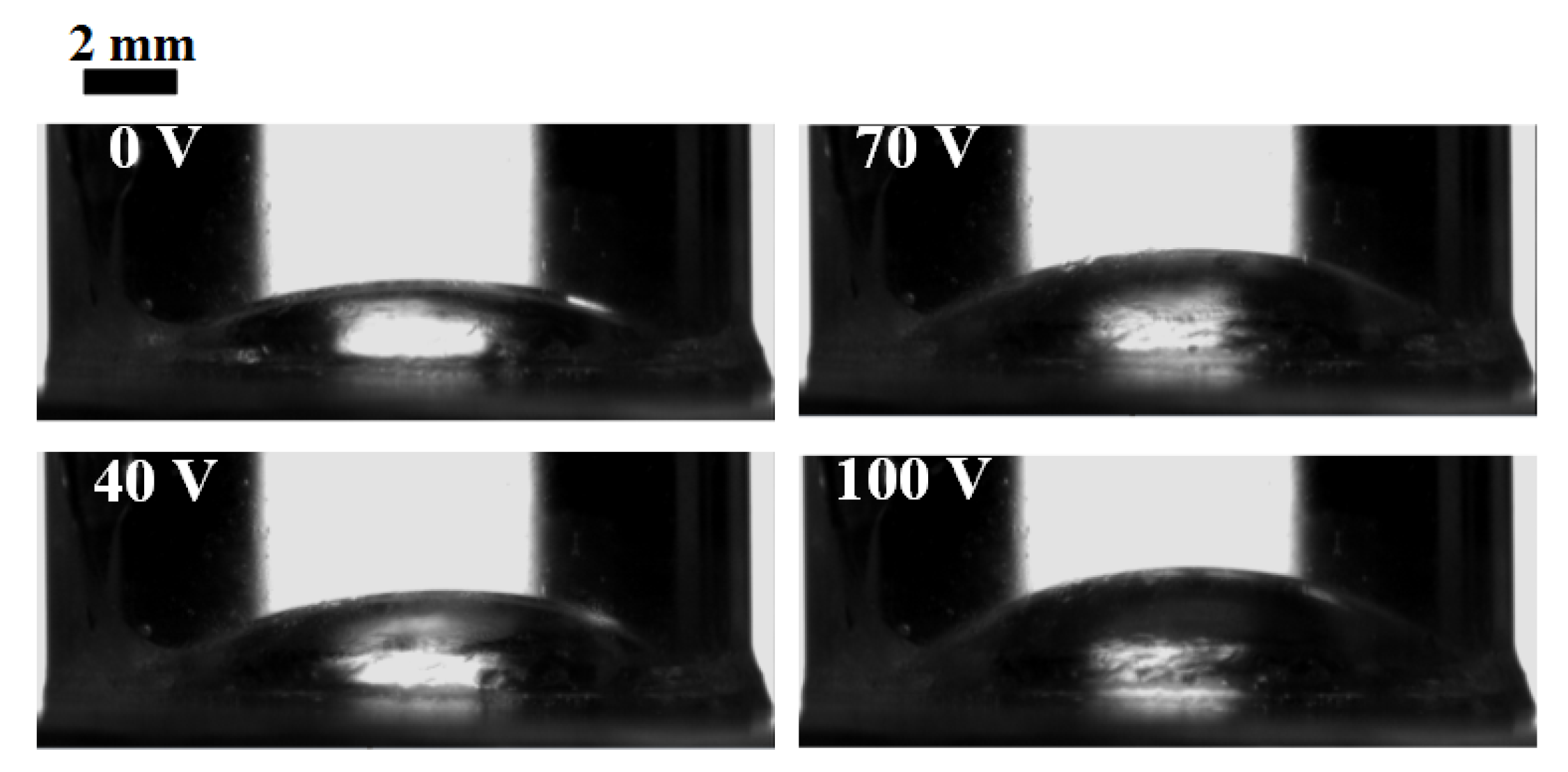
3.1. Experiment Results

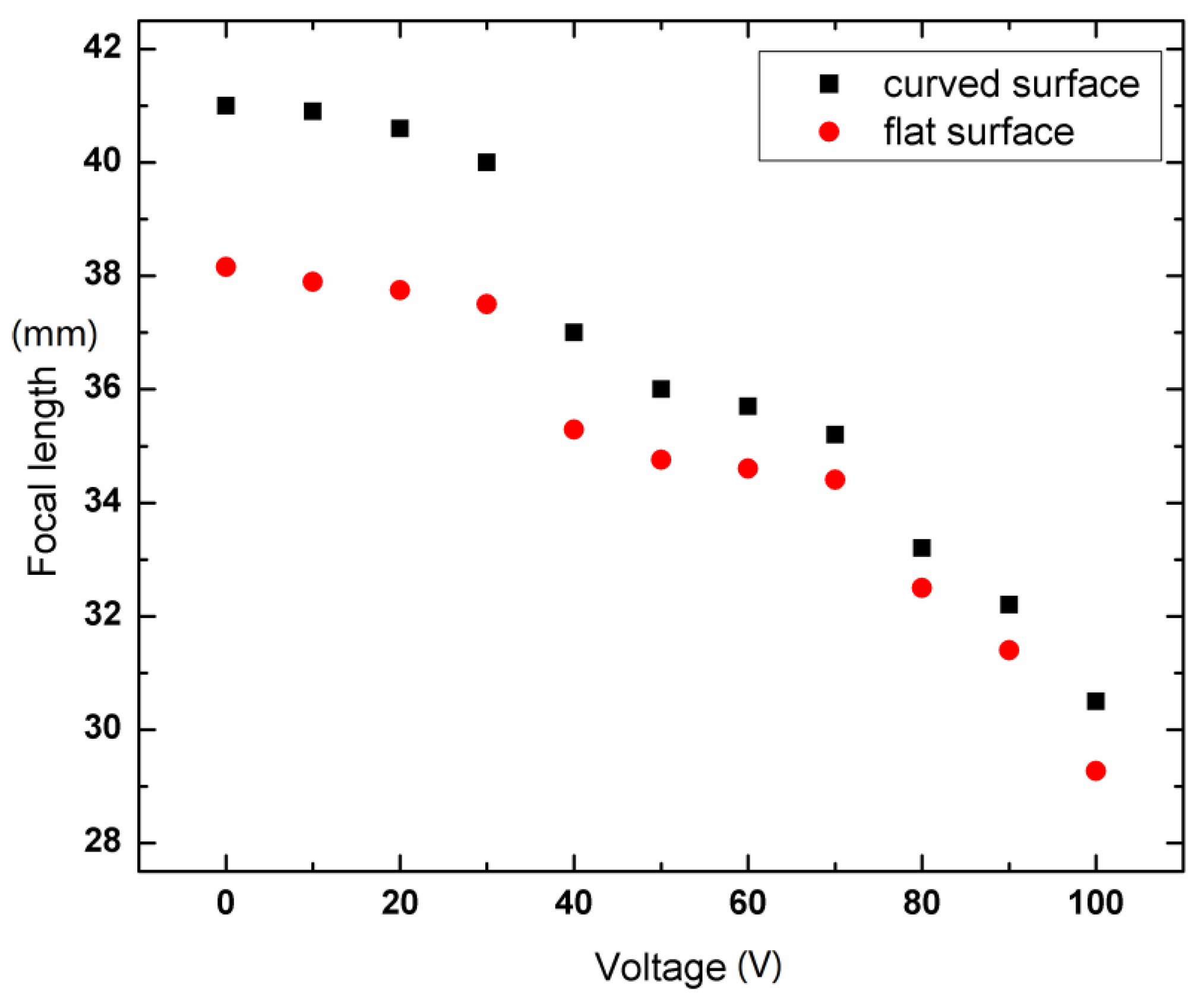
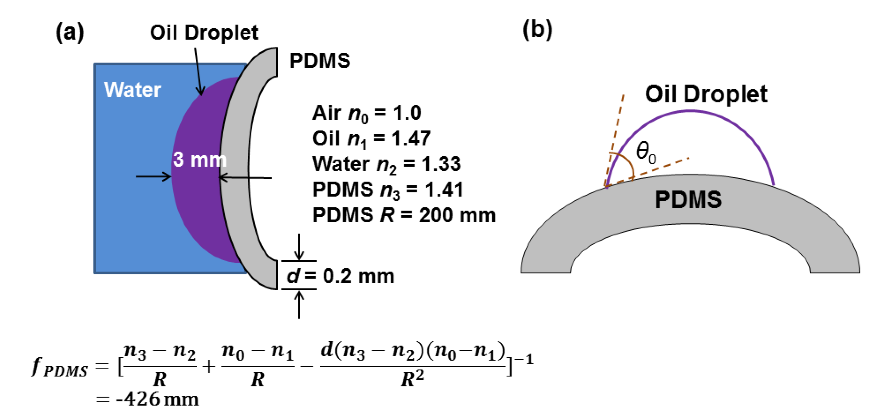
3.2. Discussion of Focal Length Change


4. Conclusions
Acknowledgments
Author Contributions
Conflicts of Interest
References
- Kuiper, S.; Hendriks, B.H.W. Variable-focus liquid lens for miniature cameras. Appl. Phys. Lett. 2004, 85, 1128–1130. [Google Scholar] [CrossRef]
- Liu, C.; Park, J.; Choi, J. A planar lens based on the electrowetting of two immiscible liquids. J. Micromech. Mcroeng. 2008, 18. [Google Scholar] [CrossRef]
- Cheng, C.C.; Chang, C.A.; Yeh, J.A. Variable focus dielectric liquid droplet lens. Opt. Express 2006, 14, 4101–4106. [Google Scholar] [CrossRef]
- Dong, L.; Agarwal, A.K.; Beebe, D.J.; Jiang, H. Adaptive liquid microlenses activated by stimuli-responsive hydrogels. Nature 2006, 442, 551–554. [Google Scholar] [CrossRef]
- Binh-Khiem, N.; Matsumoto, K.; Shimoyama, I. Polymer thin film deposited on liquid for varifocal encapsulated liquid lenses. Appl. Phys. Lett. 2008, 93. [Google Scholar] [CrossRef]
- Zhu, D.; Zeng, X.; Li, C.; Jiang, H. Focus-tunable microlens arrays fabricated on spherical surfaces. J. Microelectromech. Syst. 2011, 20, 389–395. [Google Scholar] [CrossRef]
- Kim, Y.; Park, J.H.; Choi, H.; Jung, S.; Min, S.W.; Lee, B. Viewing-angle-enhanced integral imaging system using a curved lens array. Opt. Express 2004, 12, 421–429. [Google Scholar] [CrossRef]
- IJzerman, W.L.; de Zwart, S.T.; Dekker, T. Design of 2D/3D Switchable Displays. In SID Symposium Digest of Technical Papers; Blackwell Publishing Ltd.: Hoboken, NJ, USA, 2005; pp. 98–101. [Google Scholar]
- Lee, B.; Jung, S.; Min, S.W.; Park, J.H. Three-dimensional display by use of integral photography with dynamically variable image planes. Opt. Lett. 2001, 26, 1481–1482. [Google Scholar] [CrossRef]
- Song, Y.M.; Xie, Y.; Malyarchuk, V.; Xiao, J.; Jung, I.; Choi, K.J.; Rogers, J.A. Digital cameras with designs inspired by the arthropod eye. Nature 2013, 497, 95–99. [Google Scholar] [CrossRef]
- Krupenkin, T.; Yang, S.; Mach, P. Tunable liquid microlens. Appl. Phys. Lett. 2003, 82, 316–318. [Google Scholar] [CrossRef]
- Li, C.; Jiang, H. Electrowetting-driven variable-focus microlens on flexible surfaces. Appl. Phys. Lett. 2012, 100. [Google Scholar] [CrossRef]
- Niu, X.Z.; Peng, S.L.; Liu, L.Y.; Wen, W.J.; Sheng, P. Characterizing and patterning of PDMS-based conducting composites. Adv. Mater. 2007, 19, 2682–2686. [Google Scholar] [CrossRef]
- Bowden, N.; Brittain, S.; Evans, A.G.; Hutchinson, J.W.; Whitesides, G.M. Spontaneous formation of ordered structures in thin films of metals supported on an elastomeric polymer. Nature 1998, 393, 146–149. [Google Scholar] [CrossRef]
- Eddings, M.A.; Johnson, M.A.; Gale, B.K. Determining the optimal PDMS–PDMS bonding technique for microfluidic devices. J. Micromech. Microeng. 2008, 18. [Google Scholar] [CrossRef]
- Duffy, D.C.; Schueller, O.J.; Brittain, S.T.; Whitesides, G.M. Rapid prototyping of microfluidic switches in poly (dimethyl siloxane) and their actuation by electro-osmotic flow. J. Micromech. Microeng. 1999, 9. [Google Scholar] [CrossRef]
- Rousche, P.J.; Pellinen, D.S.; Pivin, D.P., Jr.; Williams, J.C.; Vetter, R.J. Flexible polyimide-based intracortical electrode arrays with bioactive capability. IEEE Trans. Biomed. Eng. 2001, 48, 361–371. [Google Scholar] [CrossRef]
- Engel, J.; Chen, J.; Liu, C. Development of polyimide flexible tactile sensor skin. J. Micromech. Microeng. 2003, 13. [Google Scholar] [CrossRef]
- Takeuchi, S.; Ziegler, D.; Yoshida, Y.; Mabuchi, K.; Suzuki, T. Parylene flexible neural probes integrated with microfluidic channels. Lab Chip 2005, 5, 519–523. [Google Scholar] [CrossRef]
- Rodger, D.C.; Fong, A.J.; Li, W.; Ameri, H.; Ahuja, A.K.; Gutierrez, C.; Tai, Y.C. Flexible parylene-based multielectrode array technology for high-density neural stimulation and recording. Sens. Actuators B Chem. 2008, 132, 449–460. [Google Scholar] [CrossRef]
- Lee, H.; Cho, J. Development of Conformal PDMS and Parylene Coatings for Microelectronics and MEMS Packaging. In Proceedings of the ASME International Mechanical Engineering Congress and Exposition, Orlando, FL, USA, 5–11 November 2005.
- Shih, C.Y.; Harder, T.A.; Tai, Y.C. Yield strength of thin-film parylene-C. Microsys. Technol. 2004, 10, 407–411. [Google Scholar] [CrossRef]
- Hassler, C.; von Metzen, R.P.; Ruther, P.; Stieglitz, T. Characterization of parylene C as an encapsulation material for implanted neural prostheses. J. Biomed. Mater. Res. B Appl. Biomater. 2010, 93, 266–274. [Google Scholar]
- Shin, Y.S.; Cho, K.; Lim, S.H.; Chung, S.; Park, S.J.; Chung, C.; Chang, J.K. PDMS-based micro PCR chip with parylene coating. J. Micromech. Microeng. 2003, 13. [Google Scholar] [CrossRef]
- Mukhopadhyay, R. When PDMS isnʼt the best. Anal. Chem. 2007, 79, 3248–3253. [Google Scholar] [CrossRef]
- Datta, A.; Eom, I.Y.; Dhar, A.; Kuban, P.; Manor, R.; Ahmad, I.; Dasgupta, P.K. Microfabrication and characterization of Teflon AF-coated liquid core waveguide channels in silicon. IEEE Sens. J. 2003, 3, 788–795. [Google Scholar] [CrossRef]
- Wang, Y.; Zhao, Y.P. Electrowetting on curved surfaces. Soft Matter 2012, 8, 2599–2606. [Google Scholar] [CrossRef]
© 2014 by the authors; licensee MDPI, Basel, Switzerland. This article is an open access article distributed under the terms and conditions of the Creative Commons Attribution license (http://creativecommons.org/licenses/by/3.0/).
Share and Cite
Li, C.; Jiang, H. Fabrication and Characterization of Flexible Electrowetting on Dielectrics (EWOD) Microlens. Micromachines 2014, 5, 432-441. https://doi.org/10.3390/mi5030432
Li C, Jiang H. Fabrication and Characterization of Flexible Electrowetting on Dielectrics (EWOD) Microlens. Micromachines. 2014; 5(3):432-441. https://doi.org/10.3390/mi5030432
Chicago/Turabian StyleLi, Chenhui, and Hongrui Jiang. 2014. "Fabrication and Characterization of Flexible Electrowetting on Dielectrics (EWOD) Microlens" Micromachines 5, no. 3: 432-441. https://doi.org/10.3390/mi5030432
APA StyleLi, C., & Jiang, H. (2014). Fabrication and Characterization of Flexible Electrowetting on Dielectrics (EWOD) Microlens. Micromachines, 5(3), 432-441. https://doi.org/10.3390/mi5030432