Article

One-Step Combined-Nanolithography-and-Photolithography for a 2D Photonic Crystal TM Polarizer

1
Department of Electrical Engineering, The University of Texas at Dallas, Richardson, TX 75080, USA
2
Siliconfile Technologies, Inc., Seongnam-si, Gyeonggi-do 463-050, Korea
3
Department of Electrical Engineering, Korea University, Seoul 136-701, Korea
*
Author to whom correspondence should be addressed.
These authors contributed equally to this work.
Micromachines 2014, 5(2), 228-238; https://doi.org/10.3390/mi5020228
Submission received: 6 January 2014 / Revised: 15 April 2014 / Accepted: 21 April 2014 / Published: 29 April 2014
(This article belongs to the Special Issue Micro/Nano Fabrication)

Abstract

:
Photonic crystals have been widely investigated since they have great potential to manipulate the flow of light in an ultra-compact-scale and enable numerous innovative applications. 2D slab photonic crystals for the telecommunication C band at around 1550 nm have multi-scale structures that are typically micron-scale waveguides and deep sub-micron-scale air hole arrays. Several steps of nanolithography and photolithography are usually used for the fabrication of multi-scale photonic crystals. In this work, we report a one-step lithography process to pattern both micron and deep sub-micron features simultaneously for the 2D slab photonic crystal using combined-nanoimprint-and-photolithography. As a demonstrator, a 2D silicon photonic crystal transverse magnetic (TM) polarizer was fabricated, and the operation was successfully demonstrated.

Graphical Abstract

1. Introduction

Since Yablonovitch reported the first electromagnetic bandgap structure in 1987 [1], there have been tremendous efforts in studying the fundamental characteristics and the exploitation of potential applications of “photonic crystals”. Photonic crystals [2,3] are artificial crystals with periodically arranged dielectrics. Photonic crystals are capable of manipulating and controlling electromagnetic waves; they have unique optical properties that cannot be seen in conventional optical materials. Many unconventional optical properties have been found through numerous theoretical and experimental works, including negative refraction [4], superprism and supercollimation [5,6], slow light [7] and ultra-compact waveguides [8], etc. Critical feature sizes of the photonic crystals scale with the wavelength of the electromagnetic waves. For the telecommunication C band around a 1550-nm wavelength widely used in fiber optic communications, two-dimensional (2D) photonic crystals would need critical feature sizes in the deep sub-micron range [9,10], while they need to have a much larger scale (e.g., micron scale or larger) features in the same devices.
Conventional photolithography using an ultraviolet (UV) light source has been the standard technique for the fabrication of devices with critical dimension in micron and certain sub-micron scales. Furthermore, advanced photolithography technologies, such as deep UV lithography [11] and immersion lithography [12], have been developed and successfully demonstrated deep sub-100 nm-scale patterns along with larger scale structures. However, these advanced photolithography systems are rarely accessible for researchers in many research institutions. In most research institutions, electron beam lithography (EBL) or a focused ion beam (FIB) have been widely used for the fabrication of nanoscale patterns. However, since it is a serial process, electron-beam lithography takes a prohibitively long time to pattern micron or larger scale structures. Since many microelectronic or micro-optic devices with critical features in deep sub-micron scales need to have much larger scale (e.g., micron scale or even millimeter scale) features in the same devices, a combination of multi-step nanoscale lithography (e.g., electron-beam lithography or focused ion-beam) for deep sub-micron-scale patterns and photolithography for larger (e.g., from micron to millimeter) scale patterns were necessary for fabrication. Such a multi-step lithography process is undoubtedly complex, which increases the chances of failure during the device fabrication and requires numerous efforts and the time of researchers to obtain reliable samples. This research was intended to introduce a proper lithographic method to reduce the time and effort for the fabrication of multi-scale devices, such as nanophotonic crystals with micron-scale waveguides.
As an alternative to the advanced photolithography or electron-beam lithography, nanoimprint lithography (NIL) [13,14], which uses a physical molding process to replicate patterns, has attracted significant interest, due to its capability in the reliable fabrication of deep sub-100 nm-scale patterns. Since the principle of nanoimprint lithography is based on the mechanical deformation of polymer materials, even though it has been successful in replicating nanoscale structures relatively uniformly in large areas, there still remain challenges to solve for nanoimprint lithography to be a general lithographic technique. One of the biggest issues is related to the fabrication of a device with multi-scale features. Large-scale features on a nanoimprinting mold need more pressure to push viscous polymer out than smaller scale features. As a result, pattern failures or defects can be introduced in the form of inconsistent pattern heights, inconsistent residual layers or incomplete pattern transfer. In order to solve these issues, Cheng and Guo [15,16] suggested a method that combines nanoimprint lithography and photolithography processes in one step. In this method, a transparent hybrid mask mold, which integrates both a nanoimprinting mold and a metallic photomask, was used. A nanoimprinting mold is for nanoscale features, while a thin metal layer on the mold is a photomask for micron size or larger patterns. Nanoscale features are transferred into the UV curable resist layer by imprinting the hybrid mask mold, while the larger patterns are exposed to UV light through the transparent part of the mold. After detaching the mold from the sample substrate and developing, micron and nanoscale patterns can be generated in the polymer resist simultaneously. Cheng and Guo [16] called this lithographic technique combined-nanoimprint-and-photolithography (CNP).
Since CNP could decrease the number of lithographic steps and reduce the time and efforts significantly for device fabrication, we studied the CNP as a potential method to simultaneously fabricate multi-scale features in 2D silicon-based photonic crystal devices. In order to test the potential of the CNP method as a simultaneous one-step lithography, a 2D slab silicon photonic crystal transverse magnetic (TM) polarizer [10], one of our previous works, was used as an example for this work. The previous work was fabricated by a combination of conventional photolithography for micron-scale features and focused ion beam (FIB) milling for sub-micron-scale features.

2. Design of a Photonic Crystal TM Polarizer

Figure 1 shows a schematic diagram of the silicon-based 2D slab photonic crystal TM polarizer for the telecommunication C band. This particular photonic crystal has an array of air (low refractive index) holes in silicon (high refractive index). The critical dimensions of the photonic crystal are a lattice constant of 347 nm and an air hole diameter of 180 nm. In order to couple input light into the photonic crystal, a silicon input waveguide should be integrated into the photonic crystal. The input waveguide is 5~10 μm-wide and 3000 μm-long. The areas of the deflection block and photonic crystal are 24 μm × 5 μm and 24 μm × 25 μm, respectively. As shown, it is necessary to have both deep sub-micron-scale features and micron-scale features in the same device to properly operate this photonic crystal device.
Figure 1. A schematic diagram of the Si-based 2D slab photonic crystal transverse magnetic (TM) polarizer, which has both of micron-scale and sub-micron-scale features.
Micromachines 05 00228 g001
The photonic crystal was designed as a TM polarizer, which can pass TM light, but block transverse electric (TE) light in the telecommunication C band at around a wavelength of 1550 nm. As shown in Figure 2, 2D finite-difference time-domain (FDTD) simulation results showed that the photonic crystal works as a TM polarizer.
Figure 2. Finite-difference time-domain (FDTD) simulation results (a) for transverse electric (TE) light and (b) for TM light at a 1550 nm wavelength at room temperature.
Micromachines 05 00228 g002
In order to test the potential of the CNP as a method of fabrication of a 2D slab silicon photonic crystal TM polarizer, a hybrid mask mold with both a nanoscale imprinting mold and a micron-scale Cr photomask layer was made. Quartz was chosen as an imprinting mold material, since quartz substrate is known to be transparent over the 200~400 nm range of UV light and very rigid [17]. The multi-scale patterns of the photonic crystal device can be transferred to the silicon-on-insulator (SOI) sample substrate by UV exposure and imprinting, as shown in Figure 3.

3. Fabrication

3.1. Hybrid Mask Mold

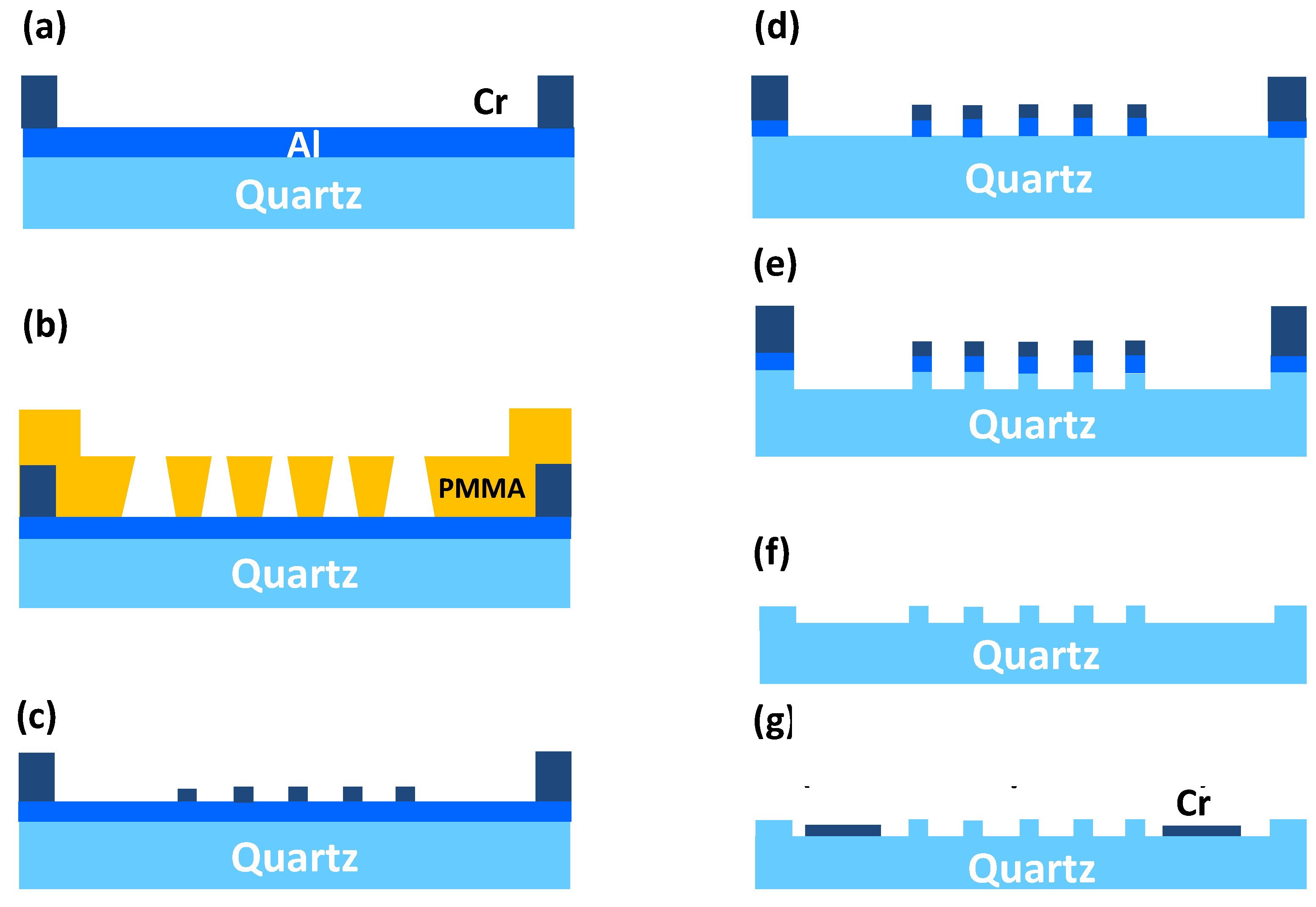
The fabrication of the hybrid mask mold was started with the deposition of a 30-nm aluminum (Al) thin film on a quartz substrate. The Al thin film layer works, firstly, as a conductive discharging layer of electrons exposed during the electron-beam lithography and, secondly, as a hard mask for the quartz substrate etching. After the aluminum deposition, S1813 photoresist was spun on the aluminum layer with a spin speed of 3000 rpm for 60 s and baked on a hotplate with 115 °C for 60 s. After the UV exposure with the exposure dose of 120 mJ/cm2, it was developed by MF-319. Then, a 100 nm-thick chromium alignment mark was formed by the lift-off process using sonication in acetone for 3 min (Figure 4a). Then, a copolymer resist was coated on top of the substrate with a spin speed of 4000 rpm for 60 s and baked on a 150-°C hotplate for 90 s. Polymethyl methacrylate (PMMA) was directly coated on the copolymer with 4000 rpm for 60 s and baked on a 180-°C hotplate for 90 s. Electron-beam lithography was carried out with an exposure dose of 300 μC/cm2 (Figure 4b). PMMA was developed using a mixed solution of isopropyl alcohol (IPA) and methyl ethyl ketone (MEK) in a ratio of 3:1 for 8 min with light agitation. Twenty nanometers-thick chromium was then deposited by using an electron-beam evaporator. After sonication in acetone, a triangular array of circular dots was formed (Figure 4c). The aluminum layer was dry etched by an inductively coupled plasma reactive ion etcher (ICP-RIE) with chlorine-based gases (15 sccm of BCl3, 5 sccm of Ar, 500 W of ICP and 30 W of bias power). Chromium dots were used as a hard mask for etching the aluminum layer. The quartz substrate was then etched to form approximately a 300 nm-tall rod array by using fluorine-based dry etching (40 sccm of CHF3, 10 sccm of Ar, 800 W of ICP and 100 W of bias power) (Figure 4e). Both the chromium and aluminum hard masks were removed by wet etch processes with commercially available CR-9S and aluminum etchant, respectively (Figure 4f). For the micron size features, the S1813 photoresist lift-off process was carried out for the formation of a 100 nm-thick chromium pattern of a micron-scale photomask, the same as the formation of the chromium alignment marks (Figure 4g). The final fabrication step of the hybrid mask mold was a conformal coating of a self-assembled monolayer (SAM) of 1H,1H,2H,2H-perfluorodecyltrichlorosilane (FDTS) on the surface of the hybrid mask mold. This is for the easy detachment from the hybrid mask mold of the resist layer after imprinting.
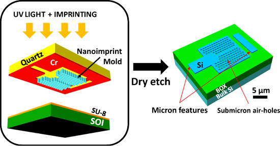
Figure 3. Schematic diagram of the combined-nanoimprint-and-photolithography (CNP) process for photonic crystal device fabrication. SOI, silicon-on-insulator.
Micromachines 05 00228 g003
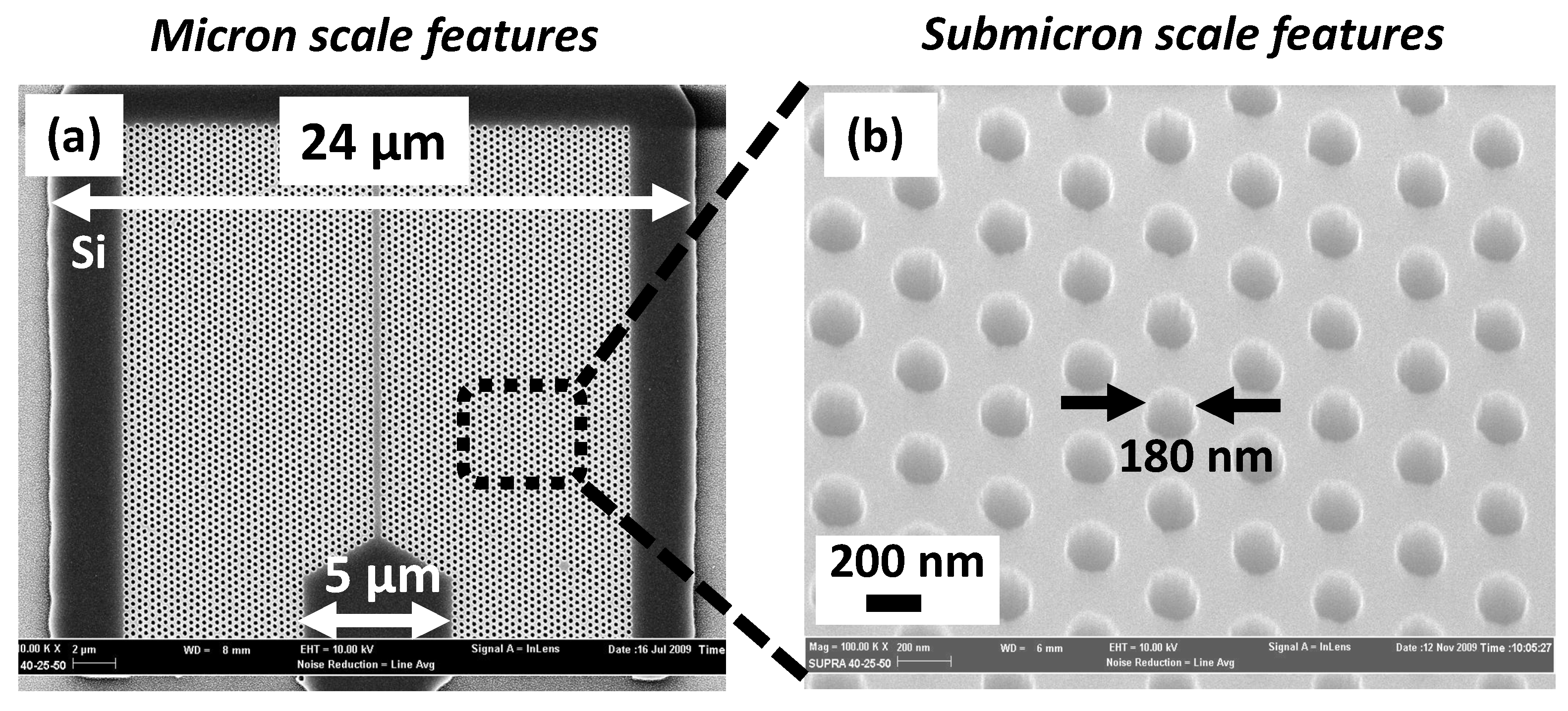
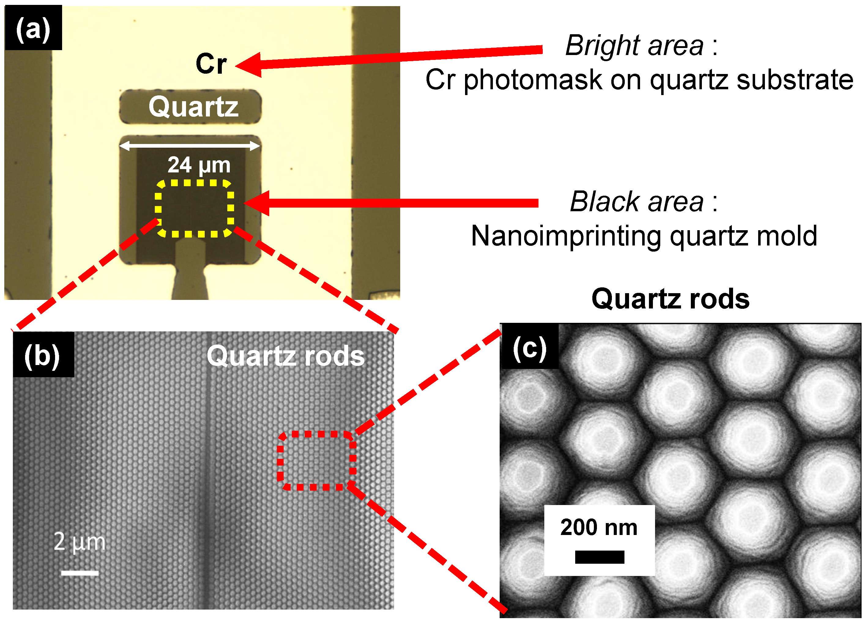
Figure 5a shows a photomicrograph of the overview of the nanoimprinting mold area. The dark brown area corresponds to a dense array of nanoscale quartz rods for the nanoimprint. The light brown area is a bare quartz area without nanoscale structures. Surrounding the light brown area, a bright chromium photomask layer defines micron-scale structures (5~24 μm) for the photolithography. The scanning electron microscope (SEM) image of a part of the nanoscale rod array in the hybrid mask mold shows an array of fairly uniform cone-shaped rods (Figure 5b,c). The rod’s flat top diameter was measured to be approximately 110 nm, while the bottom of the rod diameter was found to be 347 nm.
Figure 4. Schematic diagrams of the process sequence for the fabrication of the hybrid mask mold. (a) Cr alignment marks pattern over Al thin layer on quartz substrate, (b) PMMA and co-polymer pattern by e-beam lithography, (c) Cr dot array by lift-off, (d) Al dry etch, (e) quartz dry etch, (f) Cr and Al wet etch, and (g) micron size Cr pattern by lift-off.
Micromachines 05 00228 g004
Figure 5. (a) An optical image of the hybrid mask mold and an SEM image of (b) a dense array of quartz rods; and (c) a close-up image of the rod array.
Micromachines 05 00228 g005

3.2. Photonic Crystal TM Polarizer

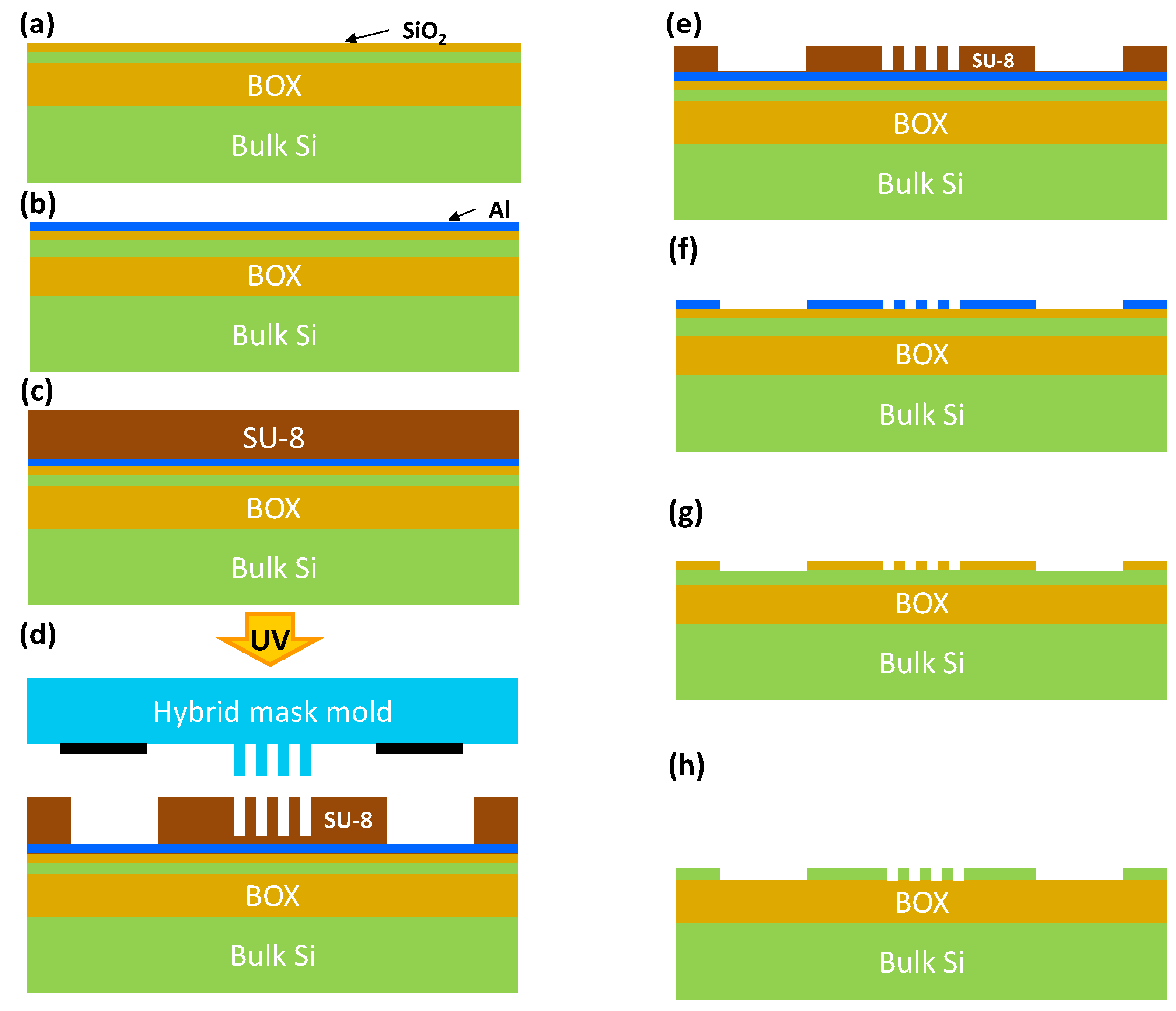
Such a hybrid mask mold was then utilized to fabricate a 2D slab silicon photonic crystal using the CNP technique. The fabrication was started with a deposition of 100 nm-thick SiO2 on a silicon layer of an SOI substrate using plasma enhanced chemical vapor deposition (PECVD) at 250 °C (Figure 6a). The aluminum layer with a thickness of 20 nm was deposited on top of the SiO2 layer by using sputtering (Figure 6b). Then, approximately a 230 nm-thick SU-8 2000.5 was spin-coated on top of the aluminum layer with a spin speed of 7000 rpm for 60 s (Figure 6c). After a sequential pre-bake of 65 °C–95 °C–65 °C on a hotplate for 1 min each, the imprinting was carried out at 85 °C with a pressure of 3 MPa for 10 min. Near the final stage of the imprinting process, the SU-8 resist was exposed by broadband UV light source (wavelengths of 200~400 nm) through the hybrid mask mold with an exposure dose of 100 mJ/cm2 at 365 nm. The hybrid mask mold was then detached, and the sample was post-baked at 65 °C–95 °C–65 °C on a hotplate for 1 min each and developed (Figure 6d). Next, the SU-8 residue layer was etched by an oxygen ICP-RIE to open the aluminum surface (50 sccm of O2 and 300 W of ICP and 100 W of bias power) (Figure 6e). Then, the aluminum layer was etched by the chlorine-based ICP-RIE process (15 sccm of BCl3, 5 sccm of Ar, 500 W of ICP and 30 W of bias power), and residual SU-8 was removed by oxygen RIE (200 mTorr of O2 pressure and 200 W of RIE power) (Figure 6f). The 100 nm-thick SiO2 layer was then etched by the fluorine-based ICP-RIE process (40 sccm of CHF3, 10 sccm of Ar, 800W of ICP and 100W of bias power), and the remaining aluminum layer was completely etched by commercially available aluminum wet etchant (Figure 6g). Finally, Si was etched by the chlorine-based ICP-RIE process (15 sccm of Cl2 and 300 W of ICP and 100 W of bias power), and residual SiO2 was removed by wet etchant by buffered oxide etchant (BOE 7:1) for 1 min (Figure 6h).
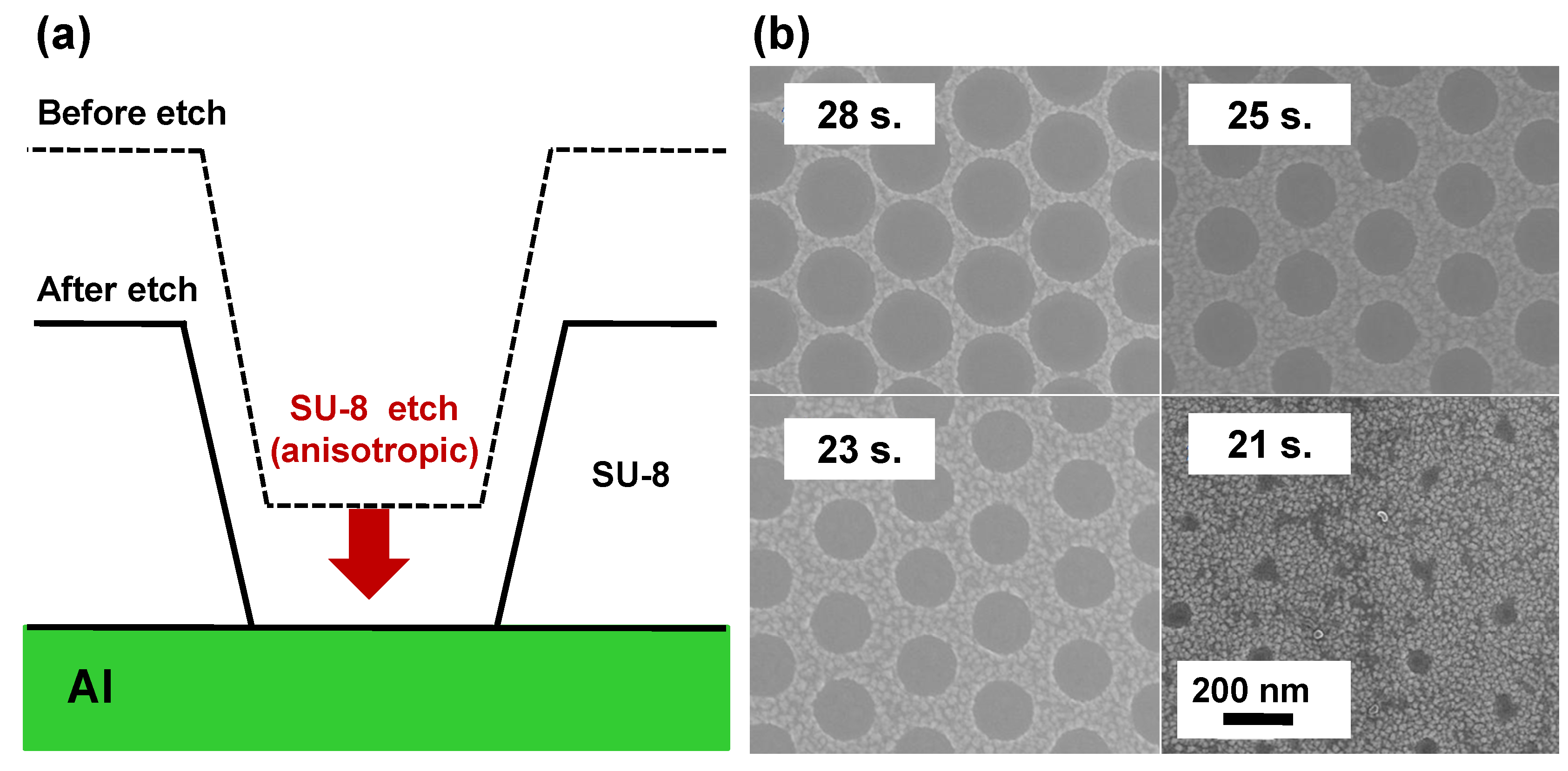
The profile of the cone-shaped rods in the hybrid mask mold was inversely replicated to SU-8 resist by the nanoimprint process. Due to the nature of the nanoimprint process, there is a thin layer of SU-8 residue at the bottom of the stamped trench, which must be removed by a subsequent O2 plasma etch process. Since the rod profile is a cone shape, it is critical to control the O2 plasma etch time to get an optimum etch profile in the SU-8 (Figure 7a). As the process time of O2 plasma etch increases, the exposed window on the aluminum hard mask becomes larger. As shown in Figure 7b, for etching times shorter than 21 s, results were not uniform and often gave irregular sizes and shapes of the window opening on the aluminum hard mask. For relatively longer etch times (greater than 22 s), fairly reproducible sizes and circular window openings were acquired.
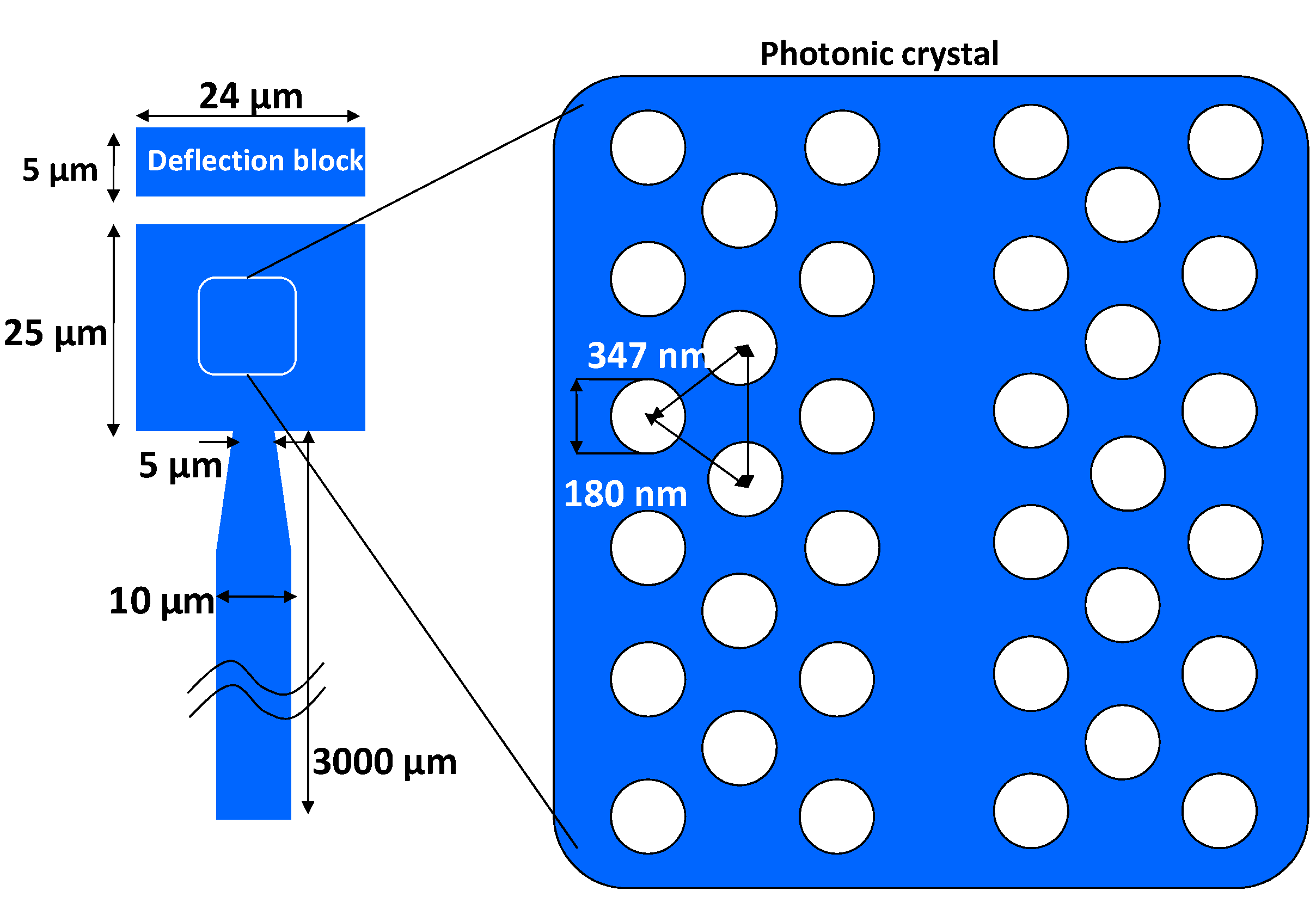
With the optimal etch profile formed in the SU-8 layer, we reliably and reproducibly fabricated fairly uniform a 180 nm-diameter air hole array with a 347-nm lattice constant in silicon (Figure 8). Figure 8a shows the final 2D slab silicon photonic crystal with a silicon waveguide. High fidelity replication of high density nanoscale features along with micron-scale features have been achieved (Figure 8).
Figure 6. Schematic diagrams of the process sequence for the fabrication of 2D slab silicon photonic crystals using combined-nanoimprint-and-photolithography. ICP-IRE, inductively coupled plasma reactive ion etcher. (a) PECVD SiO2 deposition (100 nm) on SOI substrate with 2 um-thick buried oxide (BOX) layer, (b) Al thin layer deposition (20 nm) on top of SiO2, (c) SU-8 spin-coat (230 nm) on Al layer, (d) Combined-Nanoimprint-and-Photolithography, (e) SU-8 residue dry etch, (f) Al dry etch, (g) SiO2 dry etch, and (h) silicon and SiO2 etch.
Micromachines 05 00228 g006
Figure 7. (a) Schematic diagram of the profile of the imprinted SU-8 layer and (b) an SEM image of the Al hole diameter depending on the O2 plasma etching time.
Micromachines 05 00228 g007
Figure 8. SEM images of the 2D slab silicon photonic crystal device patterned by the CNP process: (a) the overall device image showing micron-scale features; (b) a close-up 30° tilted image of the uniformly patterned air hole array showing deep sub-micron-scale features.
Micromachines 05 00228 g008

4. Characterization

In order to test if the one-step CNP-fabricated 2D slab silicon photonic crystal was working properly, the sample was characterized at room temperature using 1550-nm TE-like and TM-like polarized light. The input optical fiber tip was aligned to the cleaved input waveguide edge, so that laser light was coupled into the input waveguide. For the far-field characterization, an infrared (IR) CCD camera was used to take the top view image of the photonic crystal and associated deflection blocks, as shown in Figure 9. The far-field image of the TE-like light case (Figure 9a) shows no light spot at the interface of the TM polarizer and air, while Figure 9b shows a bright light spot at the interface for the transmitted TM-like polarized light. Figure 9 clearly shows that the photonic crystal blocks TE-like light and passes TM-like light at a 1550-nm wavelength at room temperature. This result clearly shows the multi-scale nanophotonic crystal device fabricated by the combined-nanoimprint-and-photolithography is fully functioning as designed.
Figure 9. Far-field infrared images of the top view of the TM polarizer showing (a) the blocked TE-like lights and (b) the transmitted TM-like lights at a 1.55-μm wavelength at room temperature.
Micromachines 05 00228 g009

5. Conclusions

A new lithography method for the fabrication of multi-scale 2D slab photonic crystals was demonstrated using the hybrid mask mold-enabled CNP technique. This one-step simultaneous lithography of nanoscale features along with micron-scale features significantly simplifies the fabrication process and can be widely used for the fabrication of various combined micro- and nano-scale devices. Since this process is based on the imprint process, combined micro- and nano-scale feature devices can be massively replicated until the nanoimprint mold is degraded.

Acknowledgments

The authors thank Won Park and Venkata Ananth Tamma of the University of Colorado at Boulder for carrying out the optical test for the photonic crystals and for valuable discussions of the results. This work was supported by the National Science Foundation (NSF) Nanoscale Interdisciplinary Research Team (NIRT) program under the grant, BES-0608934, and the National Research Laboratory (NRL) program (Grant No. ROA-2007-000-20111-0) of the Ministry and Science of Technology and the IT R&D program (Grant No. 2008-F-024-02, Development of Mobile Flexible IOP platform) of MKE in Korea. The manuscript preparation was funded in part by The Ministry of Science, ICT and Future Planning, Korea, under the Brain Scouting Program (HB606-12-2001) supervised by the NIPA (National IT Promotion Agency).

Author Contributions

Kyung-Hak Choi and Jinwoo Huh designed the process sequence and fabricated the devices. Yonghao Cui contributed on the design of the photonic crystal device. Krutarth Trivedi and Walter Hu contributed on nanoimprinting. Byeong-Kwon Ju and Jeong-Bong Lee guided overall research direction. Kyung-Hak Choi and Jeong-Bong Lee wrote the paper.

Conflicts of Interest

The authors declare no conflict of interest.

References

  1. Yablonovitch, E. Inhibited spontaneous emission in solid-state physics and electronics. Phys. Rev. Lett. 1987, 58, 2059–2062. [Google Scholar] [CrossRef]
  2. Joannopoulos, J.D. Photonic Crystals: Molding the Flow of Light, 2nd ed.; Princeton University Press: Princeton, NJ, USA, 2008. [Google Scholar]
  3. John, S. Strong localization of photons in certain disordered dielectric superlattices. Phys. Rev. Lett. 1987, 58, 2486–2489. [Google Scholar] [CrossRef]
  4. Luo, C.; Johnson, S.G.; Joannopoulos, J.D.; Pendry, J.B. All-angle negative refraction without negative effective index. Phys. Rev. B 2002, 65, 201104. [Google Scholar] [CrossRef]
  5. Kosaka, H.; Kaashima, T.; Tomita, A.; Notomi, M.; Tamamura, T.; Sato, T.; Kaakami, S. Superprism phenomena in photonic crystals. Phys. Rev. B 1998, 58, 10096–10099. [Google Scholar]
  6. Lupu, A.; Cassan, E.; Laval, S.; ElMelhaouri, L.; Lyan, P.; Fedeli, J.M. Experimental evidence for superprism phenomena in SOI photonic crystals. Opt. Express 2004, 12, 5690–5696. [Google Scholar] [CrossRef]
  7. Vlasov, Y.A.; O’Boyle, M.; Hamann, H.F.; McNab, S.J. Active control of slow light on a chip with photonic crystal aveguides. Nature 2005, 438, 65–69. [Google Scholar] [CrossRef]
  8. Lin, S.R.; Chow, E.; Hietala, V.; Villeneuve, P.R.; Joannopoulos, J.D. Experimental demonstration of guiding and beding of electromagnetic waves in a photonic crystal. Science 1993, 8, 928–934. [Google Scholar]
  9. Tinker, M.T.; Lee, J.-B. Thermal and optical simulation of a photonic crystal light modulator based on the thermo-optic shift of the cut-off frequency. Opt. Express 2005, 13, 7174–7188. [Google Scholar] [CrossRef]
  10. Cui, Y.; Wu, Q.; Schonbrun, E.; Tinker, M.; Lee, J.-B.; Park, W. Silicon-based 2-D slab photonic crystal TM polarizer at telecommunication wavelength. IEEE Photon. Technol. Lett. 2008, 20, 641–643. [Google Scholar] [CrossRef]
  11. Bogaerts, W.; Wiaux, V.; Taillaert, D.; Beckx, S.; Luyssaert, B.; Bienstman, P.; Baets, R. Fabrication of photonic crystals in silicon-on-insulator using 248-nm deep UV lithography. IEEE J. Sel. Top. Quantum Electron. 2002, 8, 928–934. [Google Scholar] [CrossRef]
  12. Switkes, M.; Rothschild, M. Resolution Enhancement of 157 nm Lithography by Liquid Immersion. In Proceedings of the Optical Microlithography XV Conference, Santa Clara, CA, USA, 3 March 2002; pp. 459–465.
  13. Chou, S.Y.; Krauss, P.R.; Renstrom, P.J. Imprint of sub-25 nm vias and trenches in polymers. Appl. Phys. Lett. 1995, 67, 3114–3116. [Google Scholar] [CrossRef]
  14. Aryal, M.; Trivedi, K.; Hu, W.C. Nano-confinement induced chain alignment in ordered P3HT nanostructures defined by nanoimprint lithography. ACS Nano 2009, 3, 3085–3090. [Google Scholar] [CrossRef]
  15. Cheng, X.; Guo, L.J. A combined-nanoimprint-and-photolithography patterning technique. Microelectron. Eng. 2004, 71, 277–282. [Google Scholar] [CrossRef]
  16. Cheng, X.; Guo, L.J. One-step lithography for various size patterns with a hybrid mask-mold. Microelectron. Eng. 2004, 71, 288–293. [Google Scholar] [CrossRef]
  17. Beder, E.C.; Bass, C.D.; Shackleford, W.L. Transmissivity and Absorption of Fused Quartz Between 0.22 mu and 3.5 mu from Room Temperature to 1500 degrees C. Appl. Opt. 1971, 10, 2263–2268. [Google Scholar] [CrossRef]

