Next Article in Journal
A Study on Millimetre-Wave Tunable Bandpass Filter Based on Polymer Cap Deflection
Next Article in Special Issue
Design of an Angle Detector for Laser Beams Based on Grating Coupling
Previous Article in Journal
Switchable Thermal Interfaces Based on Discrete Liquid Droplets
Previous Article in Special Issue
Multi-Beam Interference Advances and Applications: Nano-Electronics, Photonic Crystals, Metamaterials, Subwavelength Structures, Optical Trapping, and Biomedical Structures
 
 
Retraction published on 4 May 2023, see Micromachines 2023, 14(5), 1000.
Article

RETRACTED: Plasmonic Nanostructures Prepared by Soft UV Nanoimprint Lithography and Their Application in Biological Sensing

by
Grégory Barbillon
Laboratoire Charles Fabry de l’Institut d’Optique, CNRS UMR 8501, Université Paris-Sud, Campus Polytechnique, RD 128, 91127 Palaiseau Cedex, France
Micromachines 2012, 3(1), 21-27; https://doi.org/10.3390/mi3010021
Submission received: 2 December 2011 / Revised: 21 December 2011 / Accepted: 28 December 2011 / Published: 6 January 2012 / Retracted: 4 May 2023
(This article belongs to the Special Issue Nano-photonic Devices)

Abstract

:
We prepared high-density plasmonic nanostructures on a glass substrate. By using soft UV nanoimprint lithography, gold nanodisks with a diameter of 65 nm were obtained on an area of 1 mm2. We tested these gold nanosensors in the biotin/streptavidin system to study their selectivity and sensitivity of detection. The prepared gold nanodisks could detect streptavidin at 10 pM.

1. Introduction

In recent decades, in order to sense biological molecules by localized surface plasmon resonance (LSPR) on metallic nanoparticles, the capability to prepare high-density nanostructures over large areas is gaining growing importance [1,2,3]. Extinction spectroscopy measurements are mainly used to characterize these plasmonic nanostructures on an area of 100 × 100 μm2 [4,5]. In order to study multiple biomolecular interactions on a same surface, very large patterned surfaces need to be fabricated. Several techniques such as focused ion beam lithography and electron beam lithography can fabricate these large surfaces. Nevertheless, these two techniques are slow in obtaining the surfaces. Moreover, the charge effect on insulating surface can alter the regularity of the pattern shape, making these techniques unsuitable for a large-scale production. Other lithographic techniques such as extreme UV lithography [6] can also be used, but it is very expensive to fabricate their masks, which makes it difficult to render samples in ample quantity. Among the alternative methods, the soft UV nanoimprint lithography (UV-NIL) has the advantages of high speed of fabricating high-density nanostructures, low cost, and compatibility with biochemical applications [7]. Moreover, the soft UV-NIL allows fabrication at full wafer scale in one step, whereas the hard UV-NIL uses the Step-and-Flash Imprint Lithography, in which the imprint cycle is performed over a small area corresponding to one field. The fabrication with soft UV-NIL can be realized at room temperature and low pressure. However, the resolution of the fabricated molds is a limiting factor of UV-NIL [8,9]. Flexible molds in soft UV-NIL were realized by the cast molding processes, in which a suitable liquid mold material is deposited on a patterned master mold, followed by optical curing of the material. Moreover, a great homogeneity of patterns is obtained with soft UV-NIL on a large zone. In this paper, we present in detail the fabrication of plasmonic structures on glass substrates by soft UV-NIL followed by a lift-off process and their application in biological sensing. The hard polydimethylsiloxane (H-PDMS) [10,11,12] and the standard PDMS were used as soft stamp material to furnish gold nanodisks. The nanodisks have a diameter of ~65 nm, a periodicity of ~180 nm and a height of 25 nm. Finally, plasmonic sensing of streptavidin was investigated.

2. Experimental Section

2.1. Master Mold Fabrication
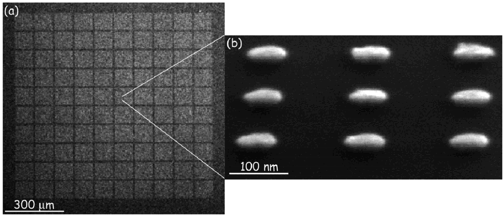
The Si master mold was fabricated by using an electron beam lithography system (Raith 150) to expose the polymethylmethacrylate A6 resist (PMMA A6) at 20 kV accelerating voltage, 7.5 μm aperture and 7 mm working distance. The patterns were then transferred into the silicon master via suitable reactive ion etching process (RIE), followed by the PMMA mask removal (Figure 1). The RIE conditions of transfer for Si are: 10 sccm for O2, 45 sccm for SF6 with P = 30 W, a pressure of 50 mTorr and an autopolarization voltage of 85 V. The obtained rates are vSi = 100 nm/min and vPMMA = 76 nm/min [13].
Figure 1. SEM images of the silicon master mold: (a) Zoom of a 100 × 100μm2 zone of nanoholes and (b) Nanoholes zone in 1 mm2.
Micromachines 03 00021 g001

2.2. Bilayer Hard-PDMS/PDMS Stamp Fabrication

To obtain better resolution and fidelity of structures in the soft UV-NIL, a bilayer H-PDMS/PDMS stamp was used. Firstly, a thin hard layer PDMS (50 μm) was spin-coated on a Si master mold [14] that was previously treated with a trimethylchlorosilane (TMCS) anti-sticking layer. Secondly, a standard PDMS (RTV 615) layer (1.5 mm) was obtained by casting on top of the H-PDMS layer. Then, the bilayer H-PDMS/PDMS stamp was degassed and cured at 75 °C for several hours. Finally, the bilayer stamp was peeled off and treated with TMCS.

2.3. Optical Characterization of Plasmonic Nanostructures

Visible extinction spectra of gold nanostructures were measured using a Jobin Yvon micro-Raman Spectrometer (Labram) in standard transmission geometry with unpolarized white light. The light illuminates the sample under normal incidence and the transmitted light is collected by an objective (×10; N.A. = 0.25) on a real area of 30 × 30 μm2. The extinction spectra were used to determine the position of the localized surface plasmon resonance of Au nanodisks and their LSPR shifts after molecular adsorption. All measurements were collected in air on freshly prepared samples to prevent atmospheric contamination.

3. Results and Discussion

3.1. Fabrication of Gold Nanodisks
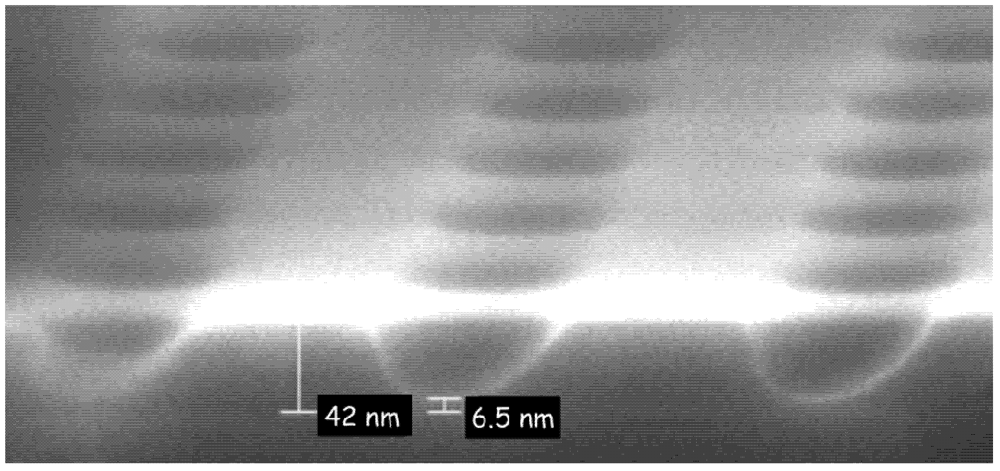
Firstly, the AMONIL resist was deposited on a PMMA lift-off layer (ThicknessPMMA = 70 nm) for the imprinting process. The AMONIL deposition had a thickness of 40 nm. Exposure to 10 mW/cm2365 nm UV for 20 minutes was used to cure the AMONIL [15]. The imprint pressure was 200 mbar. Figure 2 represents the nanoholes obtained in AMONIL. Their shapes are related to the conical dot shape of the master mold. Figure 2 shows that the AMONIL had an average diameter of ~65 nm and a residual thickness of ~6 nm. Before the PMMA etch, this residual thickness in the ground of the holes was withdrawn by a specific RIE process.
Figure 2. SEM image of the nanoholes obtained after the imprint.
Micromachines 03 00021 g002
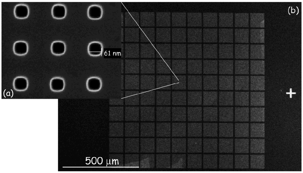
The residual AMONIL etch conditions are: 2 sccm for O2 and 20 sccm for CHF3 with a power of P = 25 W, a pressure of 7 mTorr and an autopolarization voltage of 430 V, and for the PMMA etch: 10 sccm for O2, a power of P = 10 W, a pressure of 4.7 mTorr and an autopolarization voltage of 280 V [14,16]. During the PMMA etching, a good selectivity between the PMMA and AMONIL is obtained (vPMMA/vAMONIL = 80/30 = 2.7, etch rates in nm/min) [14]. In order to realize the metallic nanodisks, an adhesion layer (Cr: 2 nm) for Au and a gold thin layer (23 nm) were successively evaporated. Figure 3 shows SEM images of gold nanodisk arrays in 1 mm2 obtained on a glass substrate.
Figure 3. SEM images of Au nanodisks with an average diameter of ~65 nm on a glass substrate: (a) Zone of 1 mm2 and (b) Zoom on 9 nanodisks of a 100 × 100μm2 pattern.
Micromachines 03 00021 g003

3.2. Plasmonic Biological Molecules Sensing

We used the biotin/streptavidin system to evaluate the sensitivity and selectivity of our LSPR-based nanoscale affinity biosensors. A simple model was first described by Campbell’s group [17]:
Δλ = mΔn [1 − exp(−2d/ld)]    (1)
where ∆λ is the wavelength shift, m is the refractive index sensitivity [18], ∆n is the change in refractive index induced by an adsorbate (∆n = nadsorbate − nair), d is the effective thickness of the adsorbate layer, and ld is the characteristic evanescent electric field decay length. The sensitivity m determined by the Finite Difference Time Domain (FDTD) method is equal to 220 nm per refractive index unit (RIU) for our gold nanodisks arrays. To evaluate ld, the electric field intensity was first calculated by FDTD for different heights from the disk’s top and then fitted according to the Prony’s method using a single exponential [3,14]. For gold nanodisk arrays ld equals 13 nm. The index difference between air and streptavidin molecule is ∆n = 0.56 [2]. The size of streptavidin molecule is around 6 nm [2,3].
Firstly, the LSPR peak of the Au nanodisk arrays was determined and λLSPR = 605 nm (Figure 4). Then, the gold nanodisks used in the detection of streptavidin were biotinylated by immersion for 2 h in a solution (1 mg·mL−1) of tri-thiolated polypeptides modified with a biotin molecule at their N-terminal end, and washed to remove all unbound molecules. Afterwards, the sample was dried with N2 gas. Next, gold nanodisks were incubated in 10 pM streptavidin solution for 3 h. Nanodisks were rinsed thoroughly with 10 mM and 20 mM PBS after biotinylation and after detection of streptavidin in order to remove non-specifically bound materials. Finally, the gold nanodisks were dried again with N2 gas. After the biotinylation step, the LSPR wavelength became λLSPR = 612 nm (Figure 4). A LSPR redshift of ∆λ = 7 nm was found, which corresponded to the biotin adsorption on the gold nanodisks. According to Figure 4, a real shift of 8 nm due to the detection of streptavidin (λLSPR = 620 nm) was found.
Figure 4. Smoothed extinction spectra of gold nanodisks at each functionalization step: (a) Au without molecular adsorption, (b) Au after adsorption of biotin and (c) Au + biotin after streptavidin detection.
Micromachines 03 00021 g004
According to Equation (1), we calculated the value of the effective thickness d to be 0.44 nm. Therefore the paving density of streptavidin can be estimated [19] to be 0.073. By comparison with the maximal paving density obtained for a compacity of the hexagonal 2D lattice (0.90), the streptavidin paving density is 8.1% of that maximal case at a concentration of 10 pM.

4. Conclusions

In this paper, high-density plasmonic nanostructures were realized on a large area (1 mm2) using the soft UV-NIL technique. The obtained dimensions of the nanodisks are 65 nm in diameter, 180 nm in periodicity and 25 nm in height with the soft H-PDMS/PDMS stamp. The plasmonic streptavidin sensing was then investigated. These plasmonic nanodisks were found to be very sensitive to biomolecules and could detect streptavidin at 10 pM. Moreover, the paving density of streptavidin adsorbed on the gold nanodisks was estimated. In summary, the soft UV nanoimprint lithography is a very promising and relatively simple method to prepare plasmonic nanosensors.

References

  1. Jensen, T.R.; Duval, M.L.; Kelly, K.L.; Lazarides, A.A.; Schatz, G.C.; Van Duyne, R.P. Nanosphere lithography: Effect of the external dielectric medium on the surface plasmon resonance spectrum of a periodic array of silver nanoparticles. J. Phys. Chem. B 1999, 103, 9846–9853. [Google Scholar]
  2. Barbillon, G.; Faure, A.C.; El Kork, N.; Moretti, P.; Roux, S.; Tillement, O.; Ou, M.G.; Descamps, A; Perriat, P.; Vial, A.; et al. How nanoparticles encapsulating fluorophores allow a double detection of biomolecules by localized surface plasmon resonance and luminescence. Nanotechnology 2008, 19, 035705. [Google Scholar]
  3. Faure, A.C.; Barbillon, G.; Ou, M.G.; Ledoux, G.; Tillement, O.; Roux, S.; Fabregue, D.; Descamps, A; Bijeon, J.L.; Marquette, C.A.; et al. Core/shell nanoparticles for multiple biological detection with enhanced sensitivity and kinetics. Nanotechnology 2008, 19, 485103. [Google Scholar]
  4. Barbillon, G.; Bijeon, J.L.; Plain, J.; Royer, P. Sensitive detection of biological species through localized surface-plasmon resonance on gold nanodisks. Thin Solid Films 2009, 517, 2997–3000. [Google Scholar] [CrossRef]
  5. Anker, J.N.; Hall, W.P.; Lyandres, O.; Shah, N.C.; Zhao, J.; Van Duyne, R.P. Biosensing with plasmonic nanosensors. Nat. Mater. 2008, 7, 442–453. [Google Scholar] [CrossRef]
  6. Dhawan, A.; Duval, A.; Nakkach, M.; Barbillon, G.; Moreau, J.; Canva, M.; Vo-Dinh, T. Deep UV nano-microstructuring of substrates for surface Plasmon resonance imaging. Nanotechnology 2011, 22, 165301. [Google Scholar]
  7. Krauss, P.R.; Chou, S.Y. Nano-compact disks with 400 Gbit/in2 storage density fabricated using nanoimprint lithography and read with proximal probe. Appl. Phys. Lett. 1997, 71, 3174–3176. [Google Scholar] [CrossRef]
  8. Jung, G.Y.; Johnston-Halperin, E.; Wu, W.; Yu, Z.; Wang, S.Y.; Tong, W.M.; Li, Z.; Green, J.E.; Sheriff, B.A.; Boukai, A.; et al. Circuit Fabrication at 17 nm Half-Pitch by Nanoimprint Lithography. Nano Lett. 2006, 6, 351–354. [Google Scholar] [CrossRef]
  9. Austin, M.D.; Zhang, W.; Ge, H.; Wasserman, D.; Lyon, S.A.; Chou, S.Y. 6 nm half-pitch lines and 0.04 μm2 static random access memory patterns by nanoimprint lithography. Nanotechnology 2005, 16, 1058–1061. [Google Scholar] [CrossRef]
  10. Schmid, H.; Michel, B. Siloxane polymers for high-resolution, high-accuracy soft lithography. Macromolecules 2000, 33, 3042–2049. [Google Scholar] [CrossRef]
  11. Shi, J.; Chen, J.; Decanini, D.; Chen, Y.; Haghiri-Gosnet, A.M. Fabrication of metallic nanocavities by soft UV nanoimprint lithography. Microelectron. Eng. 2009, 86, 596–599. [Google Scholar] [CrossRef]
  12. Chen, J.; Shi, J.; Decanini, D.; Cambril, E.; Chen, Y.; Haghiri-Gosnet, A.M. Gold nanohole arrays for biochemical sensing fabricated by soft UV nanoimprint lithography. Microelectron. Eng. 2009, 86, 632–635. [Google Scholar] [CrossRef]
  13. Hamouda, F.; Barbillon, G.; Held, S.; Agnus, G.; Gogol, P.; Maroutian, T.; Scheuring, S.; Bartenlian, B. Nanoholes by soft UV nanoimprint lithography applied to study of membrane proteins. Microelectron. Eng. 2009, 86, 583–585. [Google Scholar] [CrossRef]
  14. Barbillon, G.; Hamouda, F.; Held, S.; Gogol, P.; Bartenlian, B. Gold nanoparticles by soft UV nanoimprint lithography coupled to a lift-off process for plasmonic sensing of antibodies. Microelectron. Eng. 2010, 87, 1001–1004. [Google Scholar] [CrossRef]
  15. Hamouda, F.; Sahaf, H.; Held, S.; Barbillon, G.; Gogol, P.; Moyen, E.; Aassime, A.; Moreau, J.; Canva, M.; Lourtioz, J.M.; et al. Large area nanopatterning by combined anodic aluminum oxide and soft UV-NIL technologies for applications in biology. Microelectron. Eng. 2011, 88, 2444–2446. [Google Scholar]
  16. Hamouda, F.; Barbillon, G.; Gaucher, F.; Bartenlian, B. Sub-200 nm gap electrodes by soft UV nanoimprint lithography using polydimethylsiloxane mold without external pressure. J. Vac. Sci. Technol. B 2010, 28, 82–85. [Google Scholar] [CrossRef]
  17. Jung, L.S.; Campbell, C.T.; Chinowsky, T.M.; Mar, M.N.; Yee, S.S. Quantitative interpretation of the response of surface plasmon resonance sensors to adsorbed films. Langmuir 1998, 14, 5636–5648. [Google Scholar]
  18. Sagle, L.B.; Ruvuna, L.K.; Ruemmele, J.A.; Van Duyne, R.P. Advances in localized surface plasmon resonance spectroscopy biosensing. Nanomedicine 2011, 6, 1447–1462. [Google Scholar] [CrossRef]
  19. Pichon, B.P.; Barbillon, G.; Marie, P.; Pauly, M.; Begin-Colin, S. Iron oxide magnetic nanoparticles used as probing agents to study the nanostructure of mixed self-assembled monolayers. Nanoscale 2011, 3, 4696–4705. [Google Scholar] [CrossRef]