Study on the Wear Mechanism of a Diamond AFM Tip During Scribing of a Single-Crystal Silicon




Abstract
1. Introduction
2. Materials and Methods
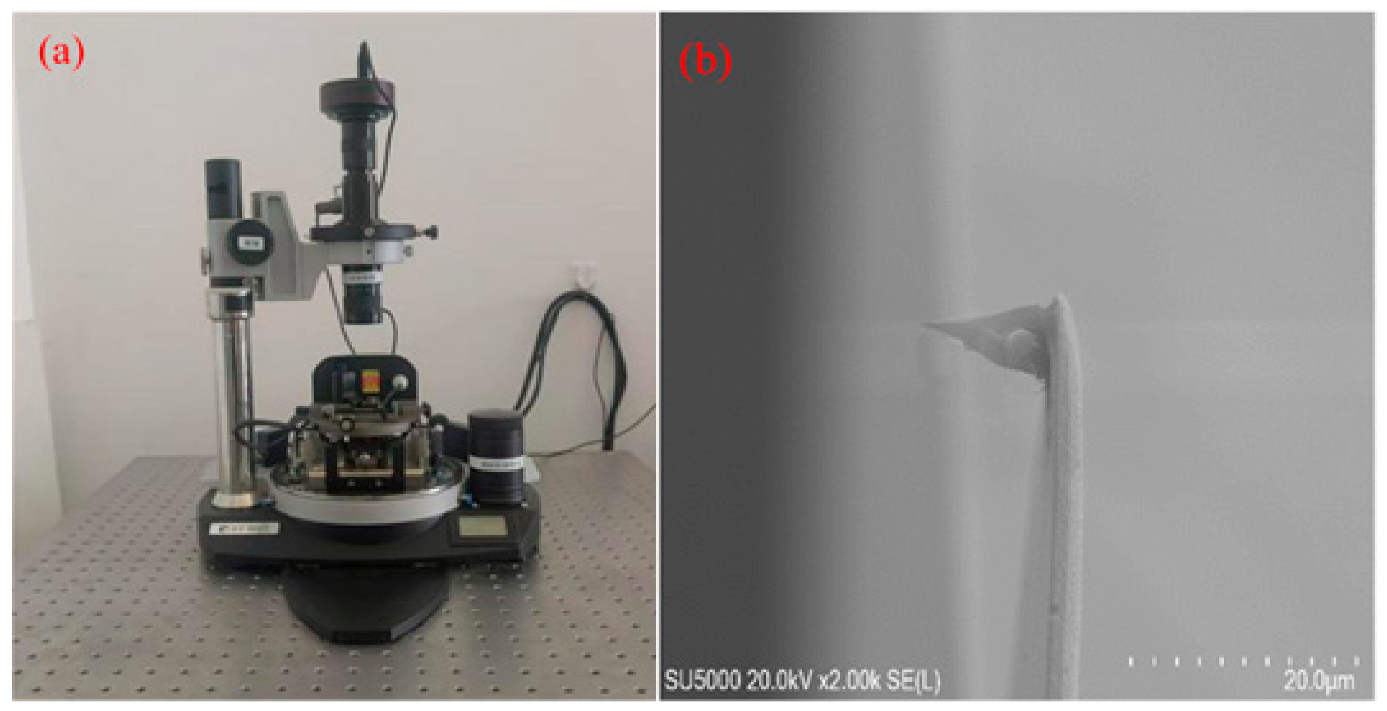
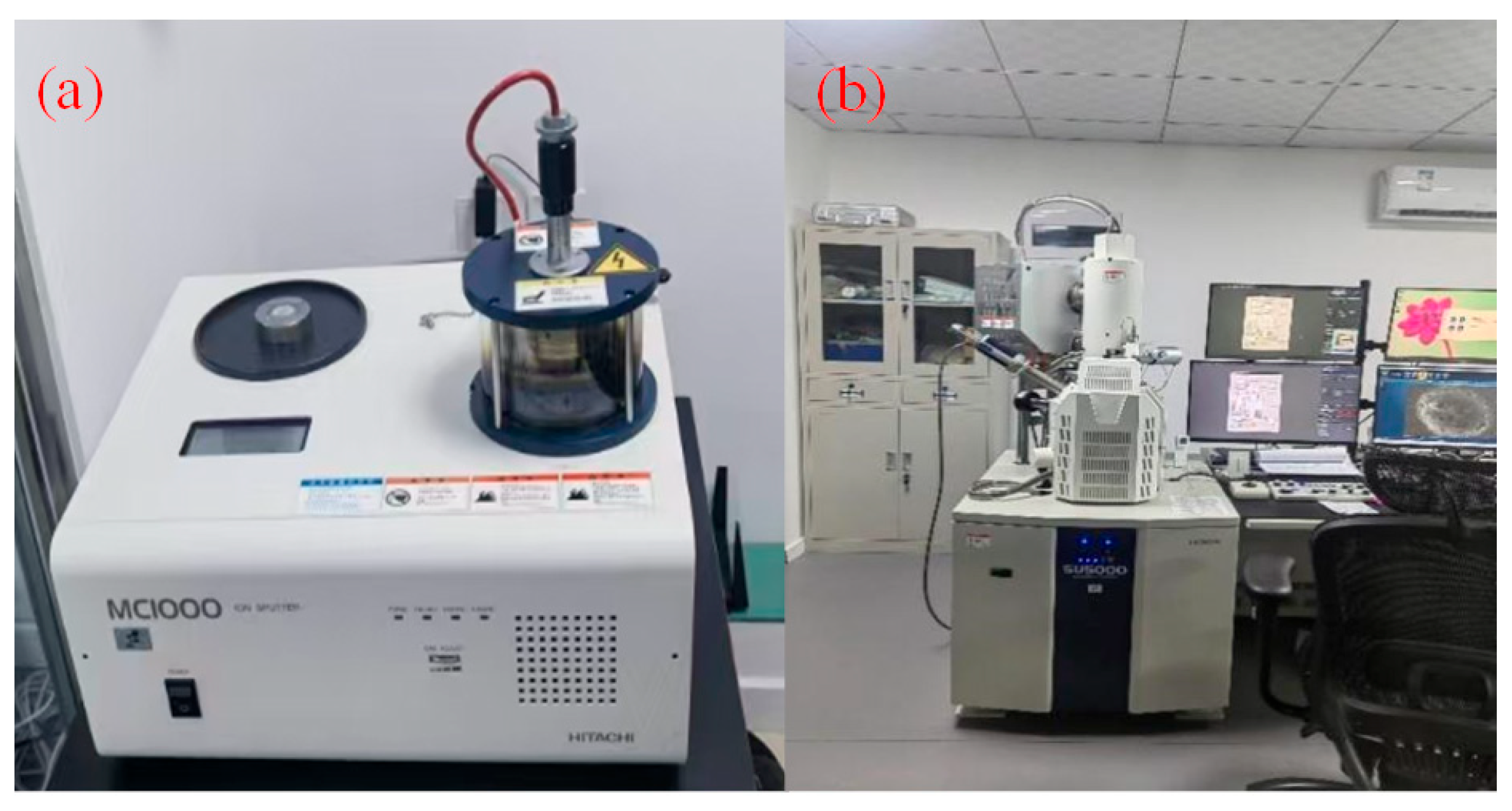
2.1. Test Equipment
2.2. Test Method
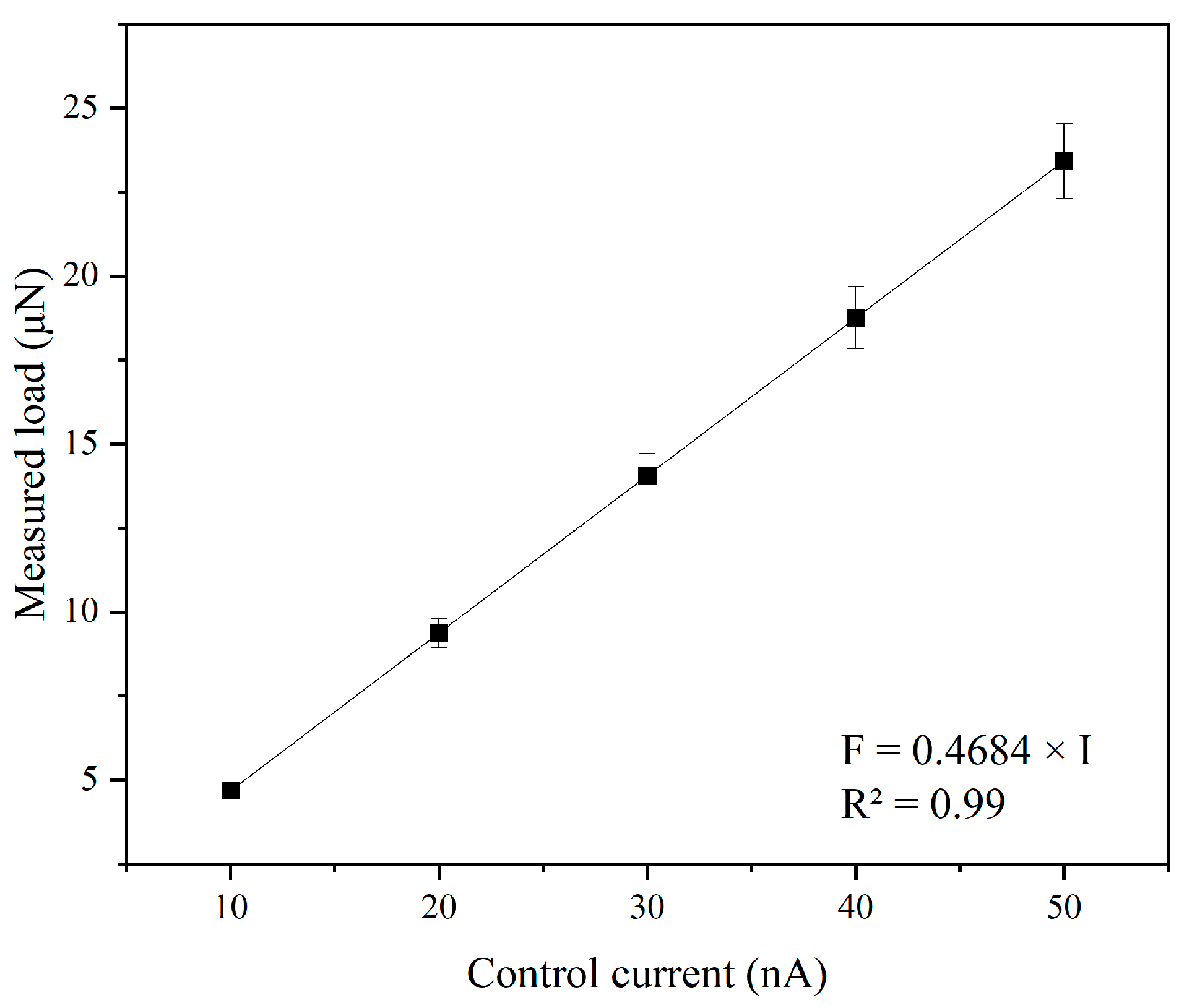
2.2.1. Current Control and Load Calibration
2.2.2. Test Protocol
2.3. Molecular Dynamics Simulation
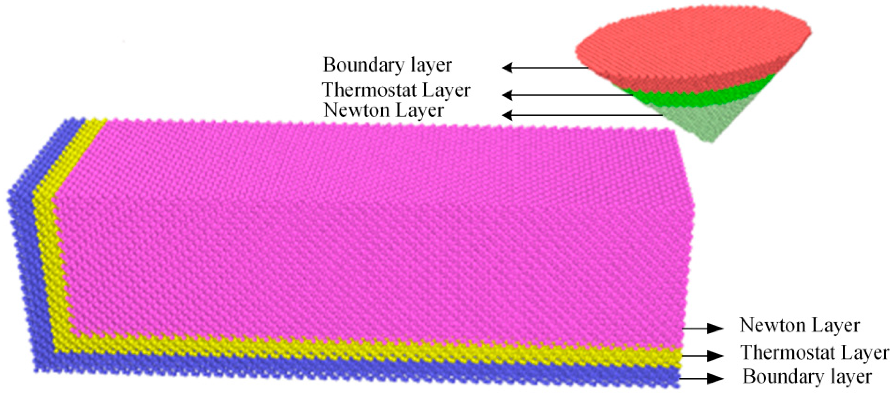
2.3.1. Model Development
2.3.2. Simulation Parameters for the Diamond Probe Scratch Test
3. Results and Discussion
3.1. Analysis of Test Results
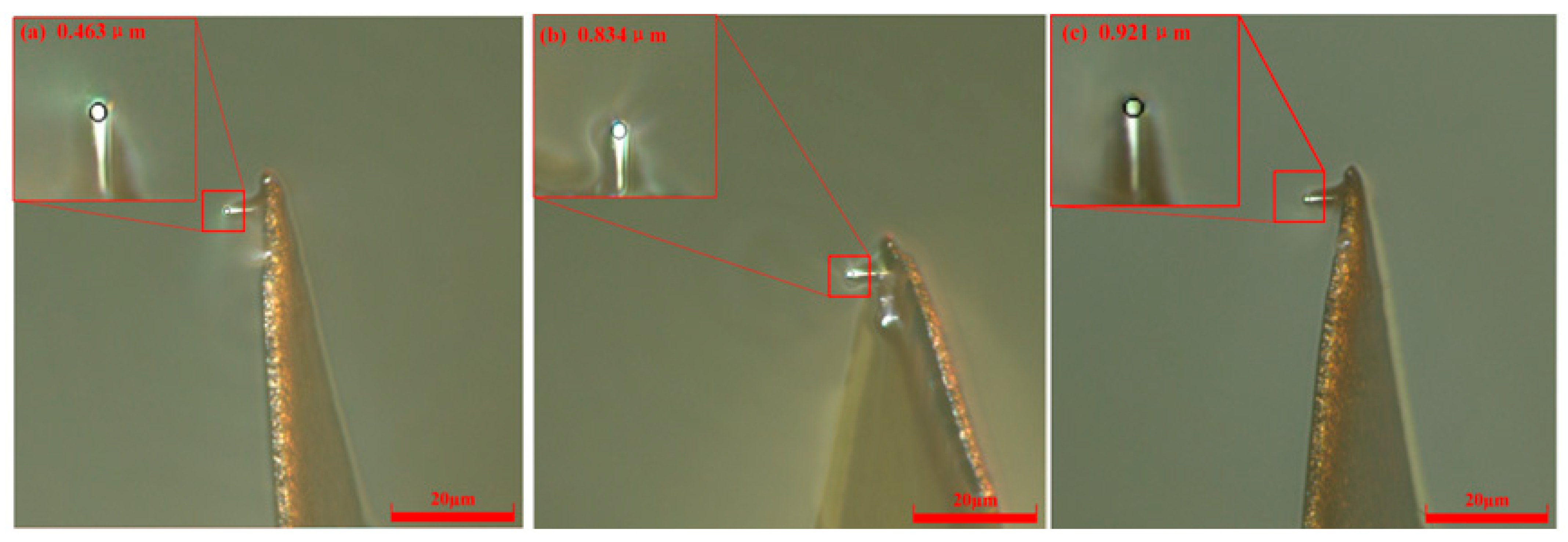
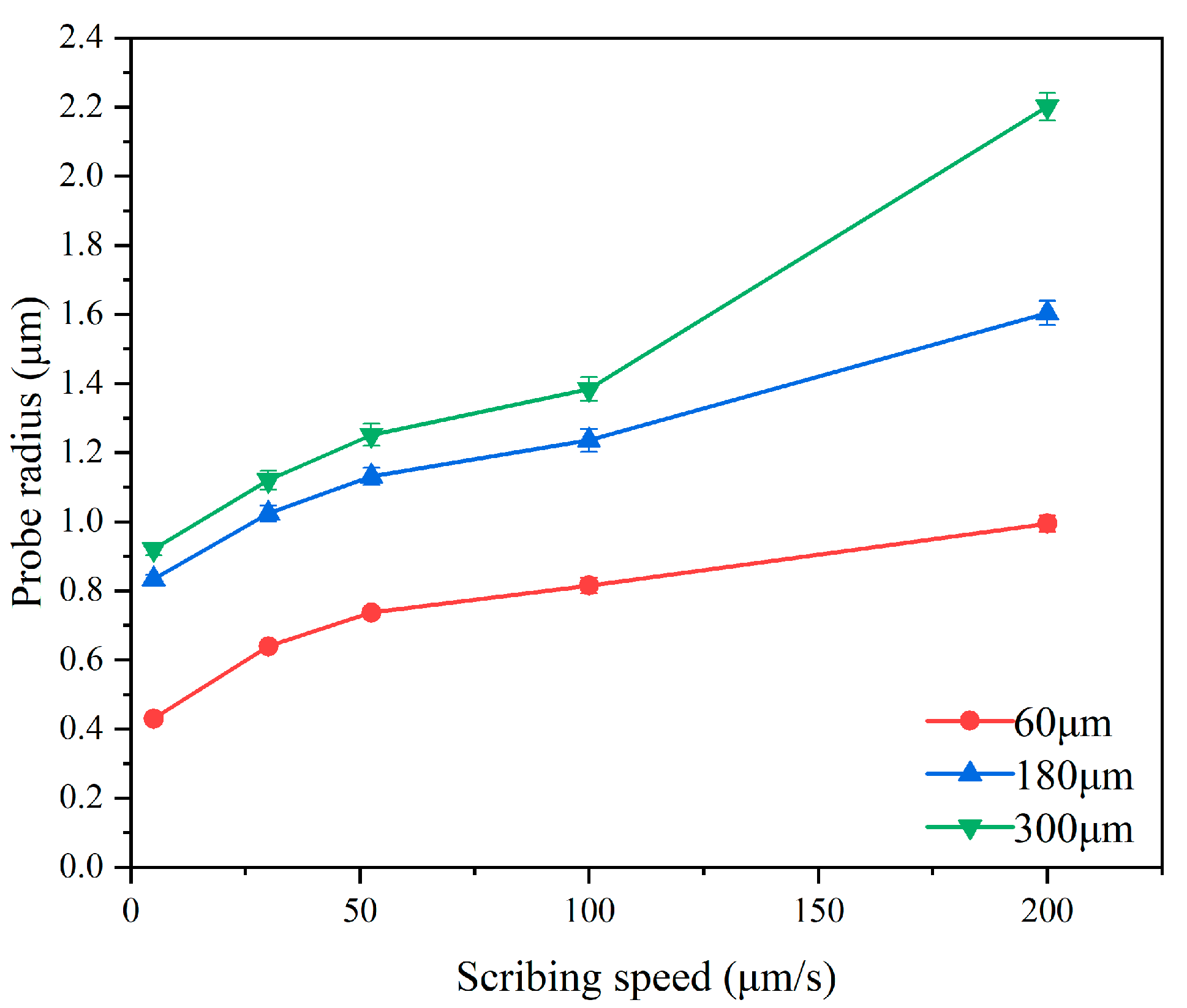
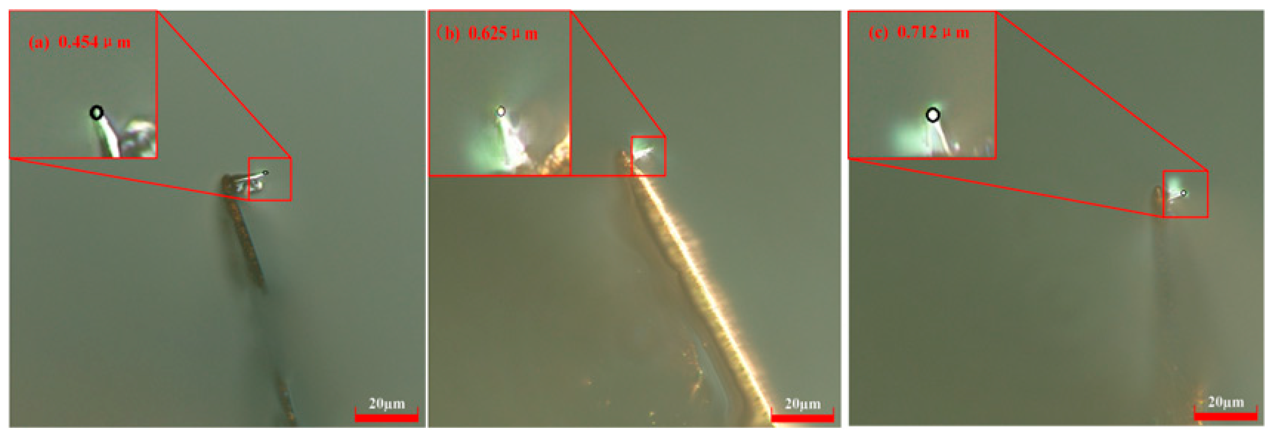
3.1.1. Analysis of Test Results at Different Scratch Speeds
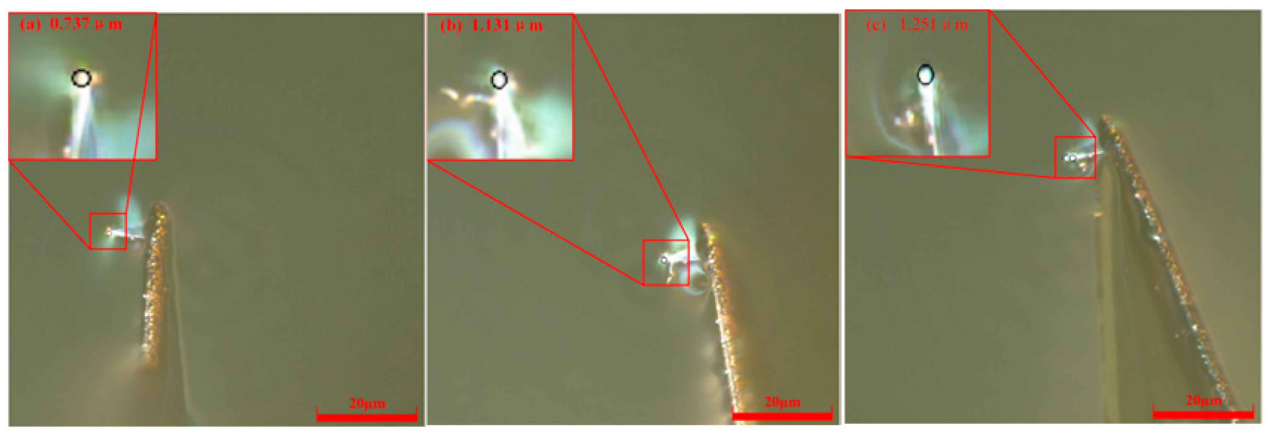
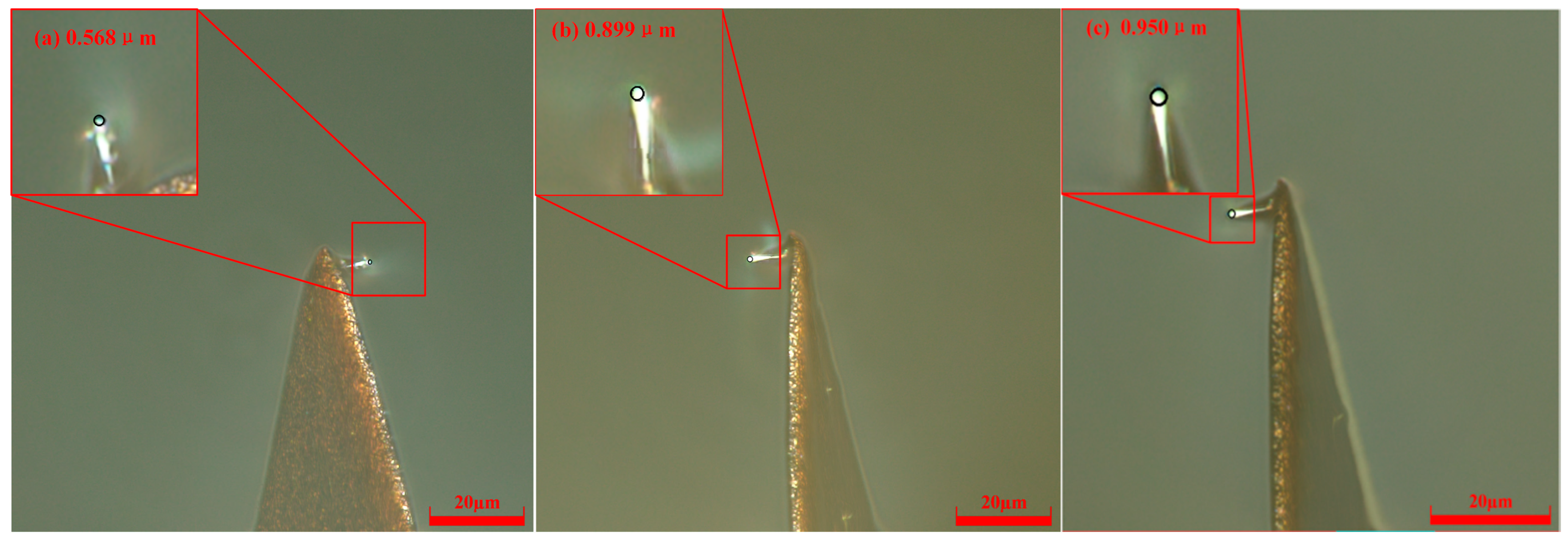
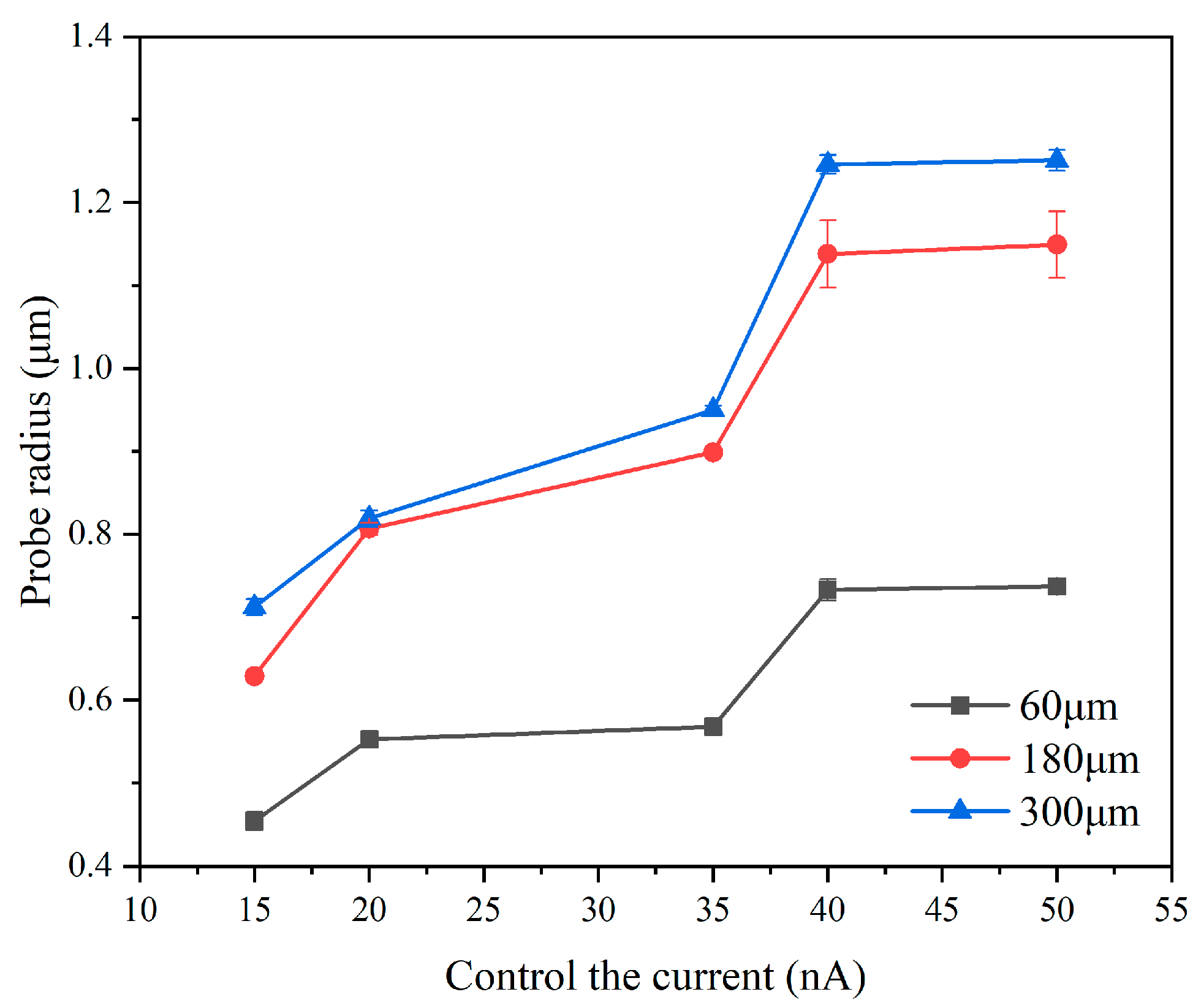
3.1.2. Analysis of Test Results Under Different Control Currents
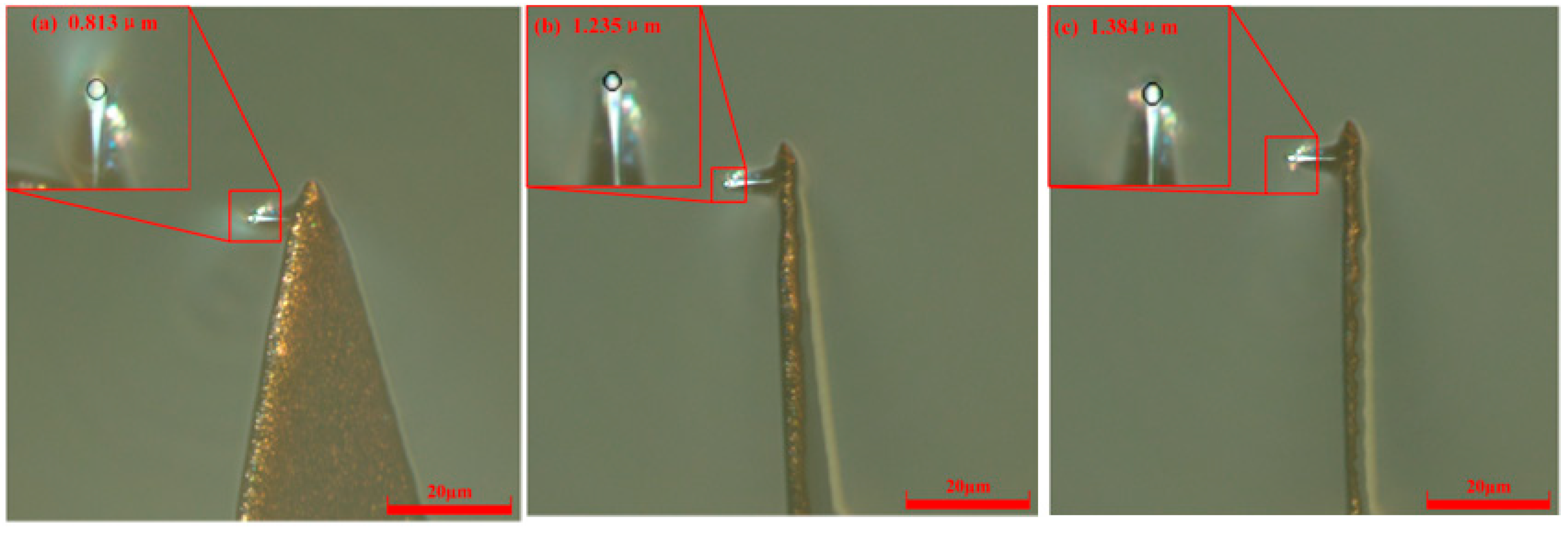
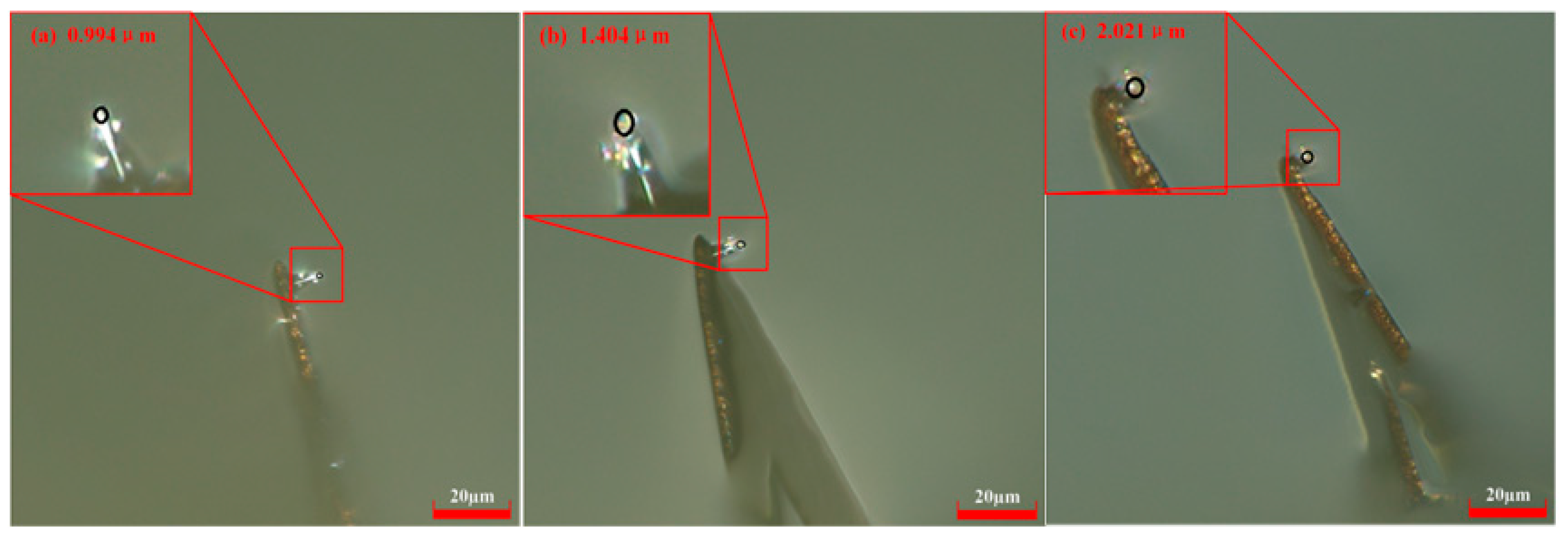
3.1.3. Analysis of Test Results at Different Scribing Distances
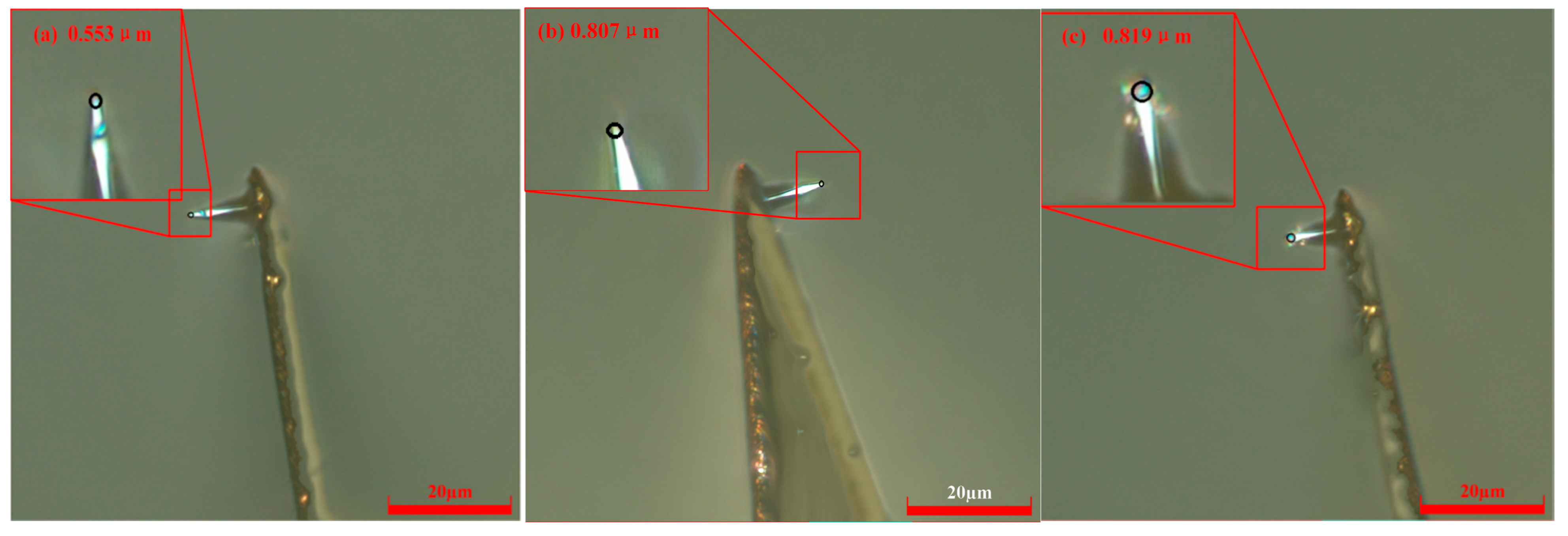
3.1.4. Verification of the Accuracy of Probe Tip Radius Measurement
3.2. Analysis of Simulation Results
3.2.1. Simulation Analysis at Different Downward Pressure Depths
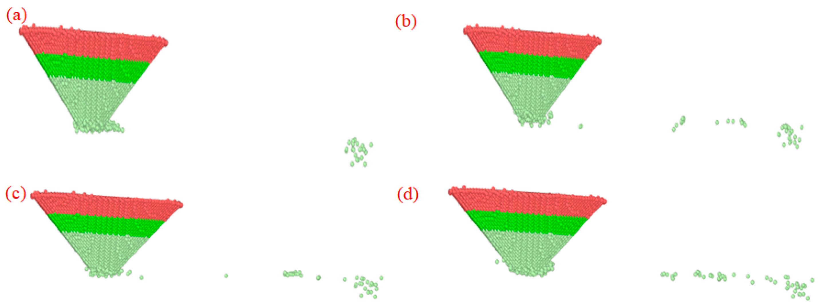
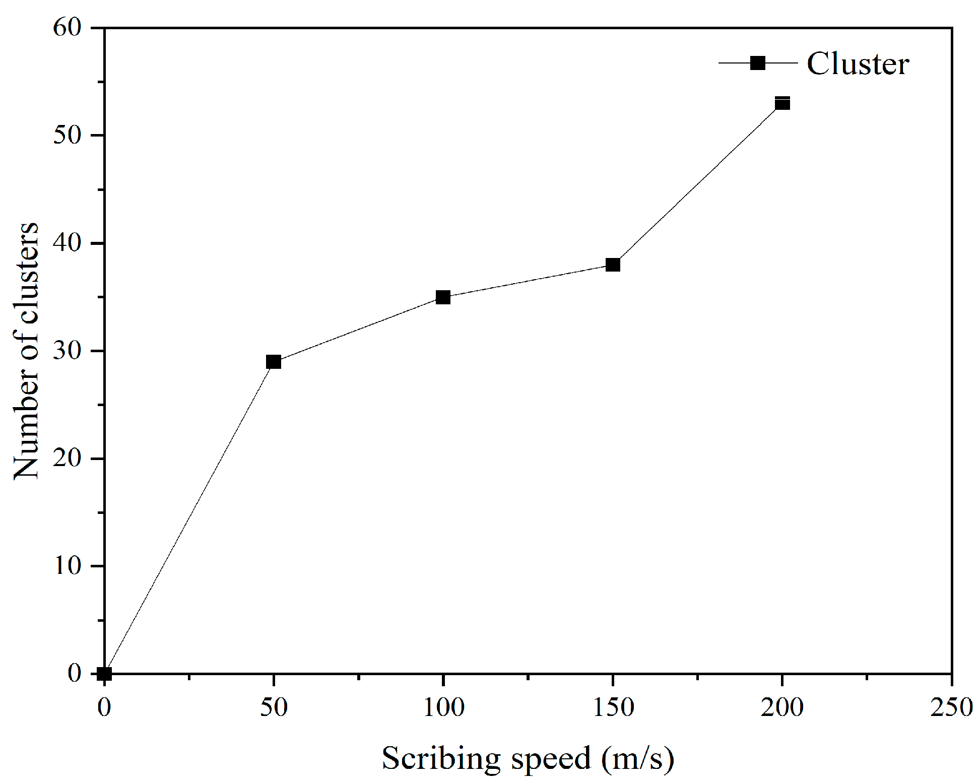
3.2.2. Simulation Analysis at Different Scribing Speeds
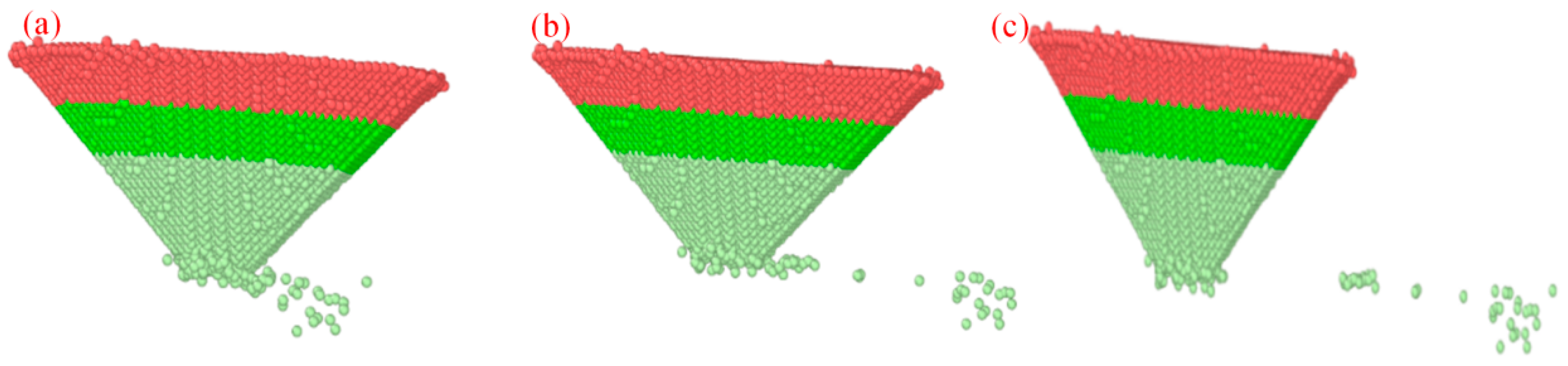
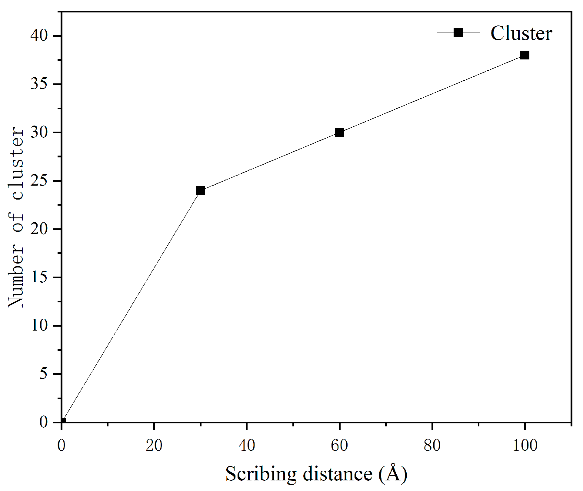
3.2.3. Simulation Analysis at Different Scribing Distances
4. Conclusions
- (1)
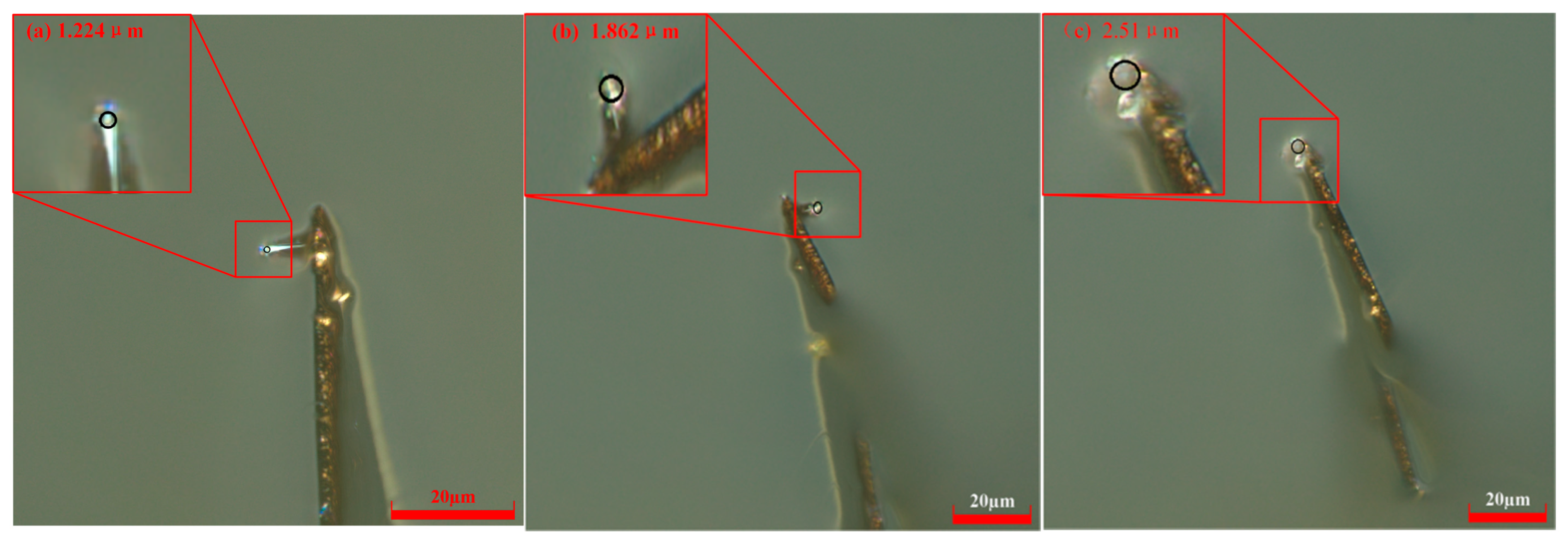
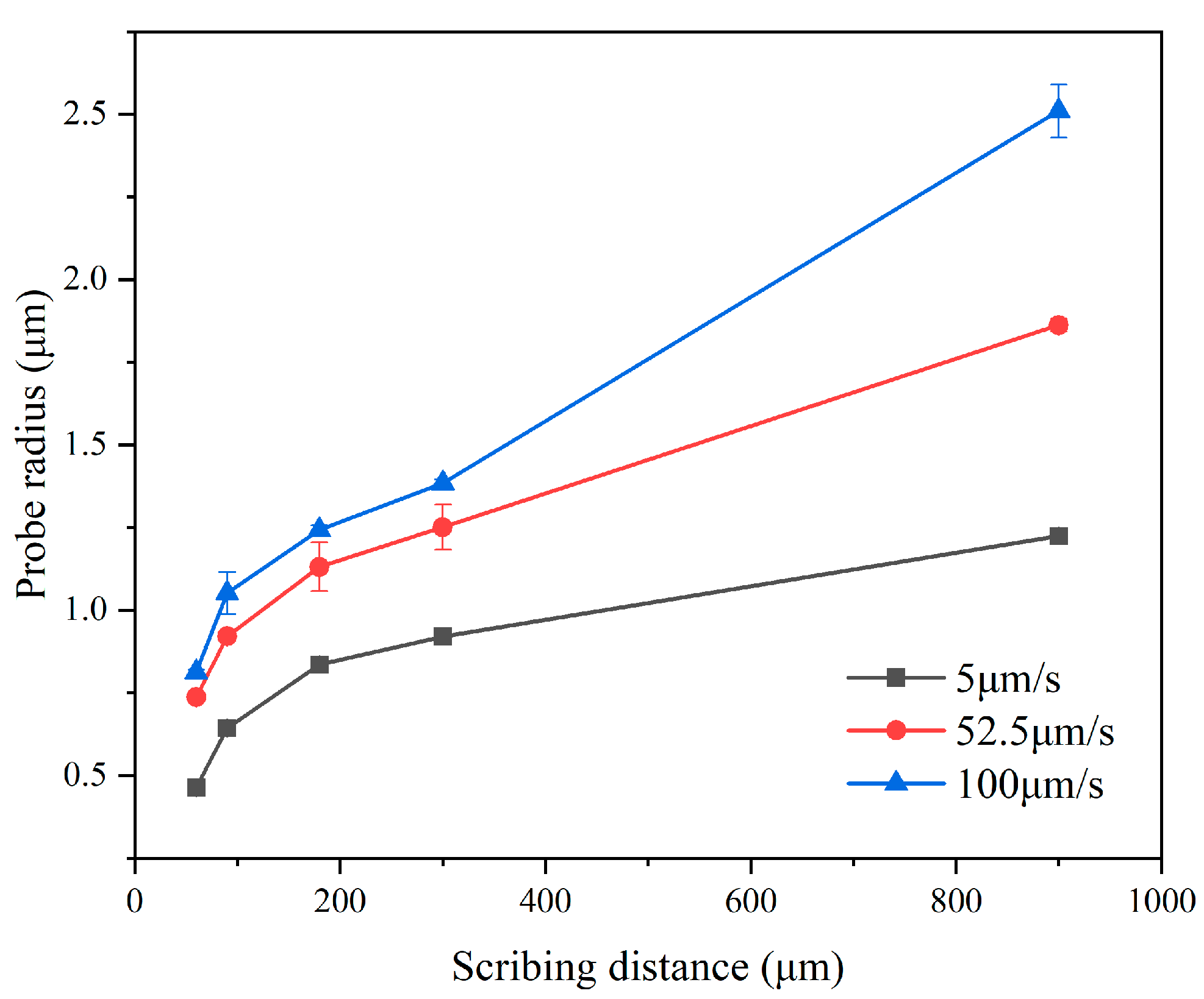
- Experimental findings demonstrate that quantitative analysis reveals a clear positive correlation between tip wear severity and three key process parameters: applied electrical current, scanning velocity, and total scratching distance. Molecular dynamics simulations also indicate that atomic attrition contributes to material loss.
- (2)
- A fully atomistic MD simulation framework was developed in LAMMPS to model the nanoscale interaction between a diamond probe and a monocrystalline silicon substrate. The simulations varied indentation depth, scribing velocity, and scribing distance. The results show that probe wear, quantified by tip radius, atomic detachment, cluster formation, and coordination number reduction, increases monotonically with each parameter. Adhesive wear, characterized by carbon–silicon interfacial bonding and carbon–carbon reattachment, occurred in all simulated conditions. This confirms its key role in diamond probe degradation during nanoscribing.
- (3)
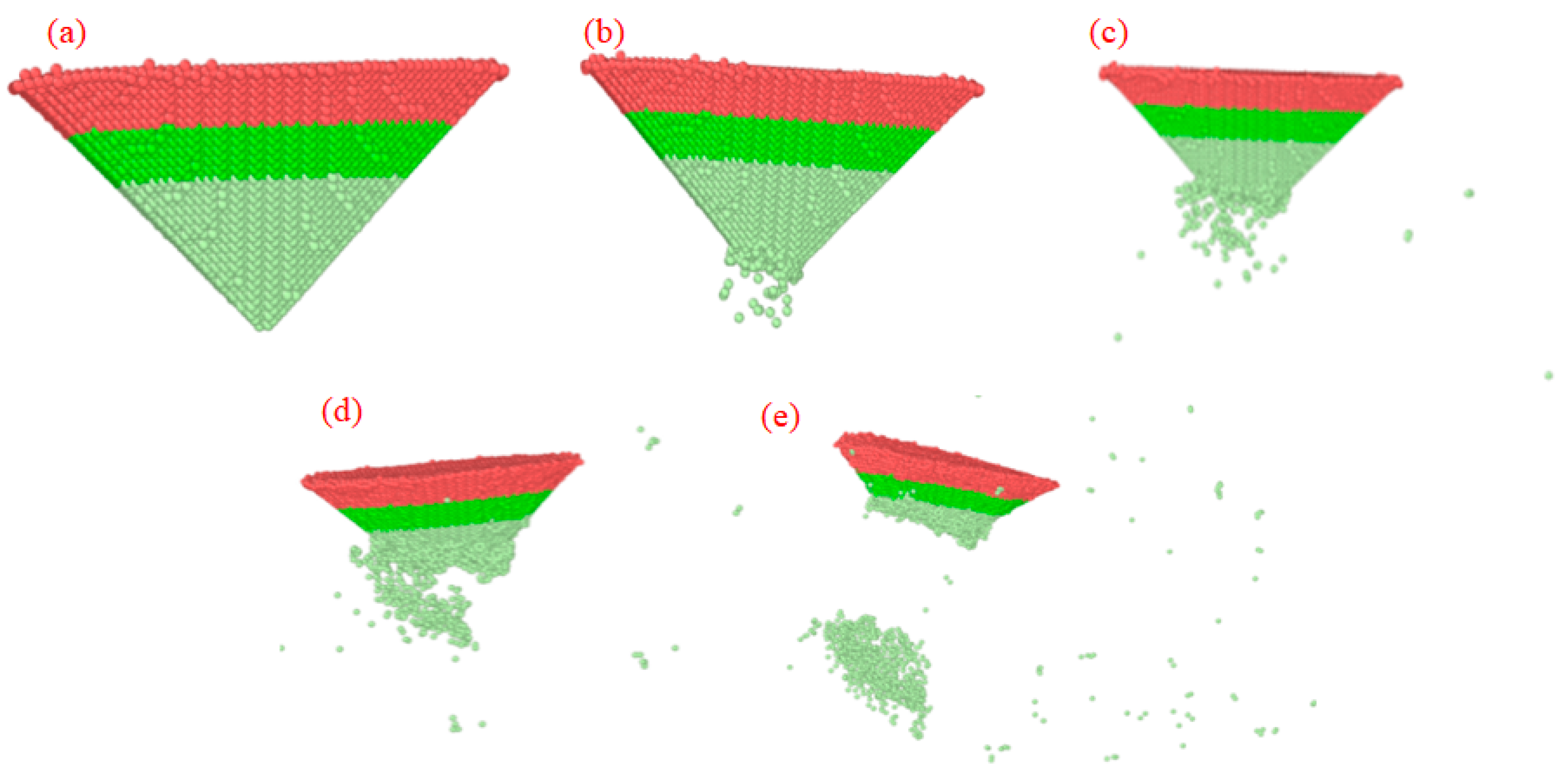
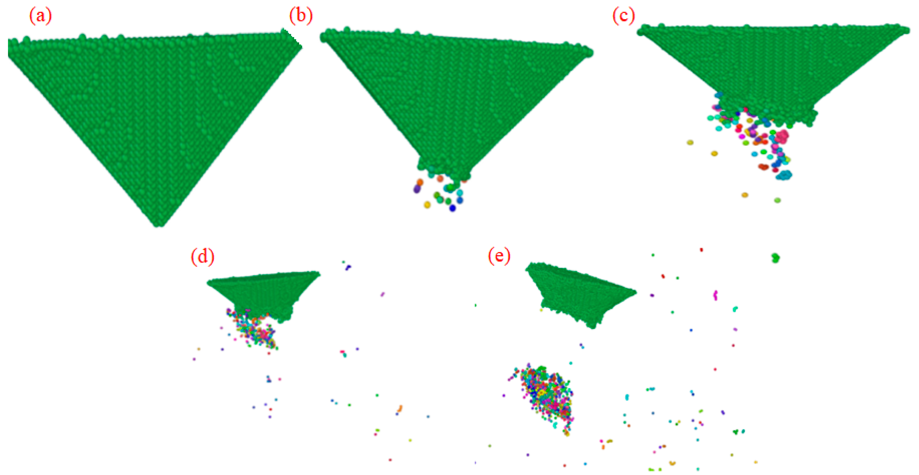
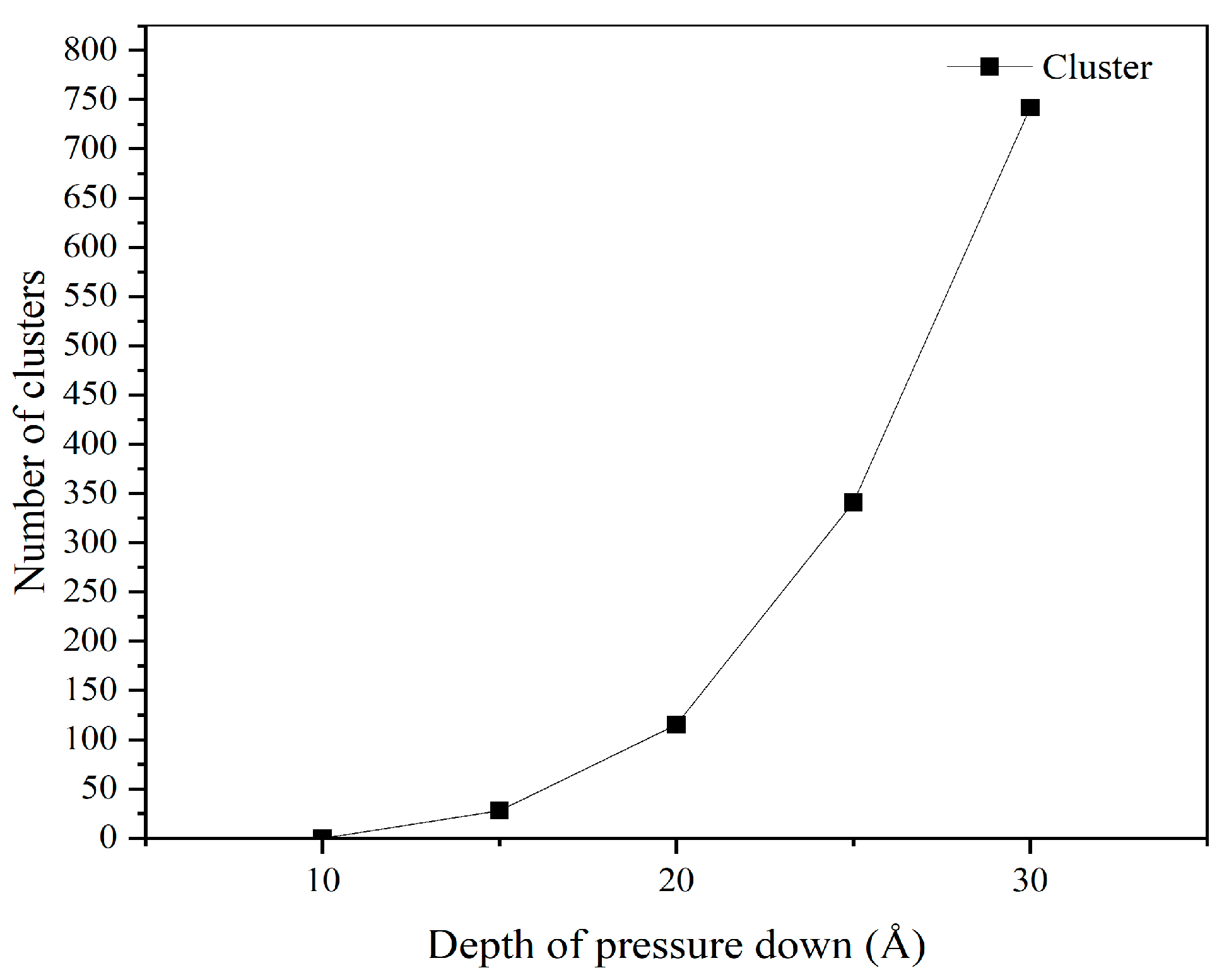
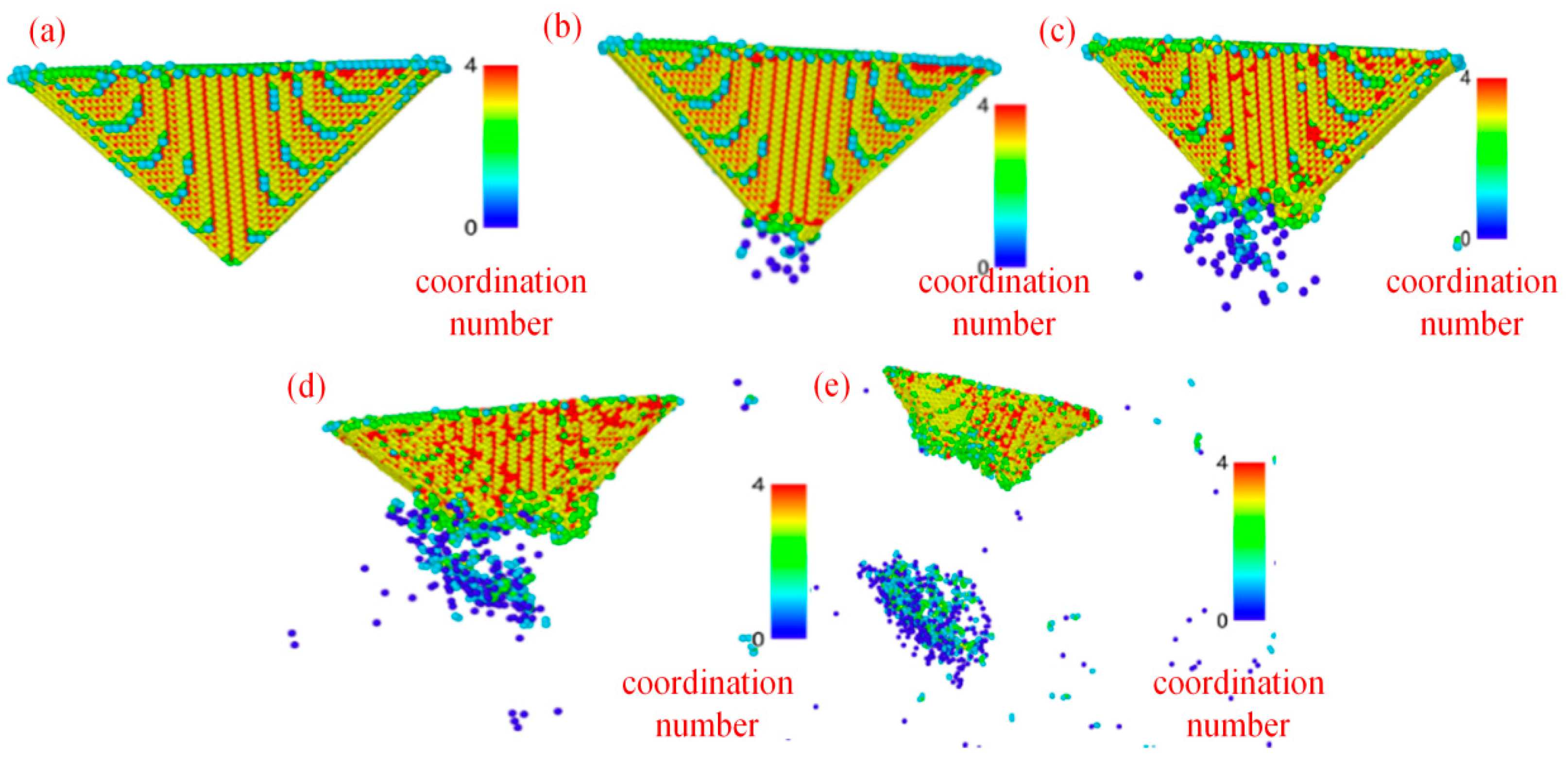
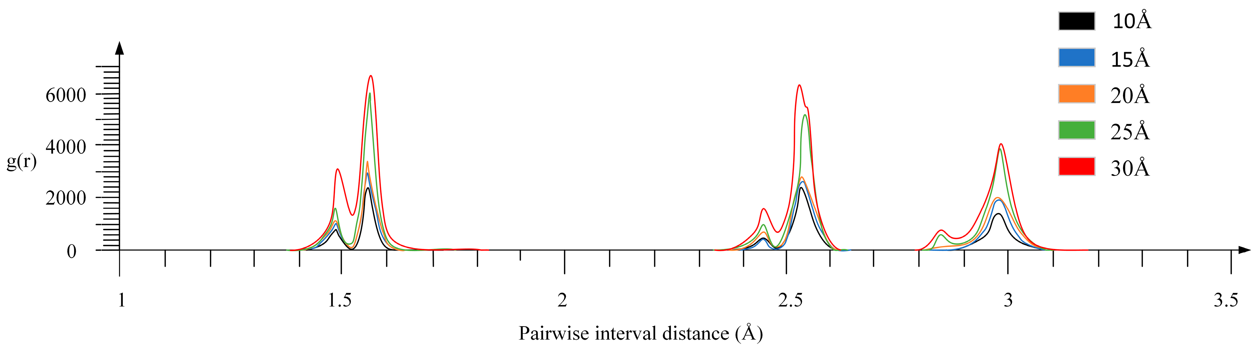
- As indentation depth increases, more atoms detach from the probe tip, leading to atom ejection. The number of atoms that transition from coordination number 4 to 3 also increases with the depth increasing, contributing to wear. At depths above 25 Å, wear changes from elastic to plastic deformation; at 30 Å, the tip deforms plastically and fractures. As scribing speed increases, atomic-level wear dominates in the early stage. With further increases in speed, the number of wear-generated clusters grows, and probe wear accelerates faster than the scribing speed. At an indentation depth of 15 Å and a scribing speed of 100 m/s, the number of detached diamond atoms increases with scribing distance.
Author Contributions
Funding
Institutional Review Board Statement
Informed Consent Statement
Data Availability Statement
Acknowledgments
Conflicts of Interest
References
- Chen, J.; Zhong, L.; Sun, J. Highly efficient nanofabrication of nanoparticle-polymer composites by AFM mechanical lithography. In Abstract Book of the 6th International Conference on Nanoscience & Technology, China; Soochow University: Suzhou, China, 2015; p. 261. [Google Scholar]
- Fan, P.; Gao, J.; Mao, H.; Geng, Y.; Yan, Y.; Wang, Y.; Goel, S.; Luo, X. Scanning probe lithography: State-of-the-art and future perspectives. Micromachines 2022, 13, 228. [Google Scholar] [CrossRef] [Scilit]
- Ercolano, G.; van Nisselroy, C.; Merle, T.; Vörös, J.; Momotenko, D.; Koelmans, W.W.; Zambelli, T. Additive manufacturing of sub-micron to sub-mm metal structures with hollow AFM cantilevers. Micromachines 2019, 11, 6. [Google Scholar] [CrossRef] [Scilit]
- Yan, Y.D.; Sun, T.; Liang, Y.C.; Dong, S. Effects of scratching directions on AFM-based abrasive abrasion process. Tribol. Int. 2008, 42, 66–70. [Google Scholar] [CrossRef] [Scilit]
- Hu, J.; He, Y.; Li, Z.; Zhang, L. On the deformation mechanism of SiC under nano-scratching: An experimental investigation. Wear 2023, 522, 204871. [Google Scholar] [CrossRef] [Scilit]
- Andrius, D.; Vytautas, B.; Darius, V.; Nikolaj, S.; Arturas, U.; Igor, I.; Inga, M.V. Modification of the AFM sensor by a precisely regulated air stream to increase imaging speed and accuracy in the contact mode. Sensors 2018, 18, 2694. [Google Scholar] [CrossRef] [Scilit]
- Kazuya, D.; Satoru, H.; Tohru, I. Effect of material type and tip radius of AFM probes on nanosheets groove machining accuracy. Adv. Mater. Res. 2010, 984, 835–842. [Google Scholar] [CrossRef] [Scilit]
- Huang, S.; Tian, Y.; Wang, T. Experimental investigation of tip wear of AFM monocrystalline silicon probes. Sensors 2023, 23, 4084. [Google Scholar] [CrossRef] [Scilit]
- Khurshudov, A.; Kato, K. Wear of the atomic force microscope tip under light load, studied by atomic force microscopy. Ultramicroscopy 1995, 60, 11–16. [Google Scholar] [CrossRef] [Scilit]
- Bloo, M.L.; Haitjema, H.; Pril, W.O. Deformation and wear of pyramidal, silicon-nitride AFM tips scanning micrometre-size features in contact mode. Measurement 1999, 25, 203–211. [Google Scholar] [CrossRef] [Scilit]
- Chung, K.-H.; Lee, Y.-H.; Kim, D.-E. Characteristics of fracture during the approach process and wear mechanism of a silicon AFM tip. Ultramicroscopy 2005, 102, 161–171. [Google Scholar] [CrossRef] [Scilit]
- Liu, C.; Zhuang, Z.; Chen, J.; Yip, W.S.; To, S. Atomic-scale investigation of Pt composition on deformation mechanism of AuPt alloy during nano-scratching process. Surf. Interfaces 2023, 40, 103126. [Google Scholar] [CrossRef] [Scilit]
- Wang, H.; Dong, Z.; Kang, R.; Gao, S. Surface characteristics and material removal mechanisms during nanogrinding on C-face and Si-face of 4H-SiC crystals: Experimental and molecular dynamics insights. Appl. Surf. Sci. 2024, 665, 160293. [Google Scholar] [CrossRef] [Scilit]
- Fan, P.; Goel, S.; Luo, X.; Yan, Y.; Geng, Y.; Wang, Y. An atomistic investigation on the wear of diamond during atomic force microscope tip-based nanomachining of gallium arsenide. Comput. Mater. Sci. 2021, 187, 110115. [Google Scholar] [CrossRef] [Scilit]
- Li, Y.; Zhang, L.; He, Y. Wear of monocrystalline silicon AFM tips under extremely high frequency tapping. Wear 2025, 571, 205809. [Google Scholar] [CrossRef] [Scilit]
- Xi, J.; Ban, X.; Ba, W.; Hui, Z.; Deng, L.; Qiu, H. Molecular dynamics simulation of scratching parameters in diamond grit scratching single-crystal silicon carbide. Mater. Sci. Semicond. Process. 2025, 199, 109838. [Google Scholar] [CrossRef] [Scilit]
- Goel, S.; Luo, X.; Reuben, R.L. Molecular dynamics simulation model for the quantitative assessment of tool wear during single point diamond turning of cubic silicon carbide. Comput. Mater. Sci. 2012, 51, 402–408. [Google Scholar] [CrossRef] [Scilit]
- Katsuki, F. Single asperity tribochemical wear of silicon by atomic force microscopy. J. Mater. Res. 2009, 24, 173–178. [Google Scholar] [CrossRef] [Scilit]
- Kopycinska-Mueller, M.; Geiss, R.H.; Hurley, D.C. Size-Related Plasticity Effects in AFM Silicon Cantilever Tips. MRS Proc. 2006, 924, 0924-Z03-02. [Google Scholar] [CrossRef] [Scilit]
- Vahdat, V.; Ryan, K.E.; Keating, P.L.; Jiang, Y.; Adiga, S.P.; Schall, J.D.; Turner, K.T.; Harrison, J.A.; Carpick, R.W. Atomic-scale wear of amorphous hydrogenated carbon during intermittent contact: A combined study using experiment, simulation, and theory. ACS Nano 2014, 8, 7027–7040. [Google Scholar] [CrossRef] [Scilit]
- Zhao, Q.L.; Dong, S.; Sun, T. Investigation of an atomic force microscope diamond tip wear in micro/nano-machining. Key Eng. Mater. 2001, 202–203, 315–320. [Google Scholar] [CrossRef] [Scilit]
- Aghajamali, A.; de Tomas, C.; Suarez-Martinez, I.; Marks, N.A. Unphysical nucleation of diamond in the extended cutoff Tersoff potential. Mol. Simul. 2018, 44, 164–171. [Google Scholar] [CrossRef] [Scilit]
- Erhart, P.; Albe, K. Analytical potential for atomistic simulations of silicon, carbon, and silicon carbide. Phys. Rev. B 2005, 71, 035211. [Google Scholar] [CrossRef] [Scilit]





| Control Current (nA) | Measured Load (μN) |
|---|---|
| 10 | 4.68 ± 0.19 |
| 20 | 9.37 ± 0.37 |
| 30 | 14.05 ± 0.56 |
| 40 | 18.73 ± 0.75 |
| 50 | 23.42 ± 0.94 |
| Scribing Velocity (μm/s) | Control Current (nA) | Scribing Distance (μm) |
|---|---|---|
| 5 | 50 | 60, 180, 300 |
| 30 | 50 | 60, 180, 300 |
| 52.5 | 50 | 60, 180, 300 |
| 100 | 50 | 60, 180, 300 |
| 200 | 50 | 60, 180, 300 |
| 52.5 | 15 | 60, 180, 300 |
| 52.5 | 20 | 60, 180, 300 |
| 52.5 | 35 | 60, 180, 300 |
| 52.5 | 40 | 60, 180, 300 |
| 52.5 | 50 | 60, 180, 300 |
| 5, 52.5, 100 | 50 | 60 |
| 5, 52.5, 100 | 50 | 90 |
| 5, 52.5, 100 | 50 | 180 |
| 5, 52.5, 100 | 50 | 300 |
| 5, 52.5, 100 | 50 | 900 |
| Parameter | Value |
|---|---|
| Probe material | Diamond |
| Probe shape | Solid cone |
| Number of probe atoms | 23,302 |
| Probe tip angle (°) | 90 |
| Height (Å) | 50 |
| Parameter | Value |
|---|---|
| Sample material | Monocrystalline silicon |
| Sample shape | Cuboid |
| Number of sample atoms | 123,981 |
| Sample surface orientation | [100] (100) |
| Sample dimensions (Å) | 300 × 90 × 150 |
| Name | Parameter |
|---|---|
| Probe material | Diamond |
| Workpiece material | Monocrystalline silicon |
| Probe shape | Cone |
| Substrate dimensions (X × Y × Z)(Å) | 300 × 90 × 150 |
| Indentation depth (Å) | 10, 15, 20, 25, 30 |
| Scribing velocity (m/s) | 10, 50, 100, 150 |
| Scribing distance (Å) | 30, 60, 100 |
| Initial temperature (K) | 298 |
| Total number of atoms | 147,283 |
| Indentation Depth/Å | Count of 3-Fold Coordinated Atoms | Number of Atoms Transformed to Coordination Number 4 |
|---|---|---|
| 10 | 0 | 0 |
| 15 | 32 | 106 |
| 20 | 187 | 481 |
| 25 | 1648 | 2349 |
| 30 | 6360 | 8047 |
Disclaimer/Publisher’s Note: The statements, opinions and data contained in all publications are solely those of the individual author(s) and contributor(s) and not of MDPI and/or the editor(s). MDPI and/or the editor(s) disclaim responsibility for any injury to people or property resulting from any ideas, methods, instructions or products referred to in the content. |
© 2026 by the authors. Licensee MDPI, Basel, Switzerland. This article is an open access article distributed under the terms and conditions of the Creative Commons Attribution (CC BY) license.
Share and Cite
Lin, X.; Qi, L.; Han, J. Study on the Wear Mechanism of a Diamond AFM Tip During Scribing of a Single-Crystal Silicon. Micromachines 2026, 17, 344. https://doi.org/10.3390/mi17030344
Lin X, Qi L, Han J. Study on the Wear Mechanism of a Diamond AFM Tip During Scribing of a Single-Crystal Silicon. Micromachines. 2026; 17(3):344. https://doi.org/10.3390/mi17030344
Chicago/Turabian StyleLin, Xinyue, Litao Qi, and Jinguo Han. 2026. "Study on the Wear Mechanism of a Diamond AFM Tip During Scribing of a Single-Crystal Silicon" Micromachines 17, no. 3: 344. https://doi.org/10.3390/mi17030344
APA StyleLin, X., Qi, L., & Han, J. (2026). Study on the Wear Mechanism of a Diamond AFM Tip During Scribing of a Single-Crystal Silicon. Micromachines, 17(3), 344. https://doi.org/10.3390/mi17030344