Article

A Wideband D-Band Frequency Sextupler Chain with High Harmonic Rejection in 100 nm GaAs pHEMT Technology

State Key Laboratory of Millimeter Waves, School of Information Science and Engineering, Southeast University, Nanjing 210096, China
*
Author to whom correspondence should be addressed.
Micromachines 2025, 16(9), 984; https://doi.org/10.3390/mi16090984
Submission received: 10 July 2025 / Revised: 17 August 2025 / Accepted: 27 August 2025 / Published: 27 August 2025

Abstract

This paper presents a wideband D-band frequency sextupler chain implemented in a 100 nm GaAs pHEMT process. The proposed circuit comprises an input-stage frequency tripler, an inter-stage harmonic-rejection power amplifier, and an output-stage frequency doubler. The tripler adopts a balanced topology, which effectively suppresses the fundamental frequency component. The inter-stage power amplifier not only delivers sufficient drive power to the doubler but also enhances suppression of undesired harmonics. The output doubler employs a single-balanced configuration to suppress odd-order harmonics while extracting the second harmonic. The measured peak output power of the sextupler chain is 2.33 dBm, corresponding to an input power of 2 dBm, resulting in a conversion gain of 0.33 dB. The 3 dB output bandwidth spans from 126.3 to 152.7 GHz, corresponding to a relative bandwidth of 18.9%. Owing to the balanced multiplier topology and harmonic-rejection PA, the 5th and 7th harmonics are suppressed by more than 20 dBc. The combination of high output power, wide operating bandwidth, and excellent harmonic suppression makes the design well suited for wideband D-band signal generation in diverse applications.

1. Introduction

With the rapid development of mobile communication technologies, particularly the widespread deployment of 5G and the upcoming 6G systems, spectrum resources are becoming increasingly scarce. Consequently, research into millimeter-wave (mmWave) frequency bands has become increasingly important [1,2]. Within this domain, the D-band has emerged as a key research focus in mmWave communications due to its substantial available bandwidth [3,4].
D-band signal generation is typically realized by cascading a low-frequency source with frequency multipliers [5]. However, undesired harmonic signals generated within the multiplier can degrade the spectral purity of the output. These spurious harmonics are usually suppressed using filters [6]. Nevertheless, in broadband frequency multiplier designs, some undesired harmonics may fall within the target frequency band, rendering conventional filtering less effective.
In this paper, a wideband D-band frequency sextupler chain in a 100 nm GaAs pHEMT process is designed. Both the cascaded frequency tripler and doubler adopt balanced topologies, which inherently suppress unwanted harmonics. A harmonic rejection PA is adopted as well. This configuration eliminates the reliance on additional filters and enhances suitability for broadband applications. The frequency sextupler chain exhibits a peak output power of 2.33 dBm with a 3 dB bandwidth from 126.3 to 152.7 GHz. The circuit topology is given in Section 2 and the measurement results are presented in Section 3.

2. Circuit Design

As shown in Figure 1, the architecture of the frequency sextupler chain is presented. The tripler is employed as the input stage, while the doubler serves as the output stage. A power amplifier is inserted to provide sufficient drive power for the doubler and to suppress the unwanted harmonics from the tripler.

2.1. Design of the Balanced Tripler

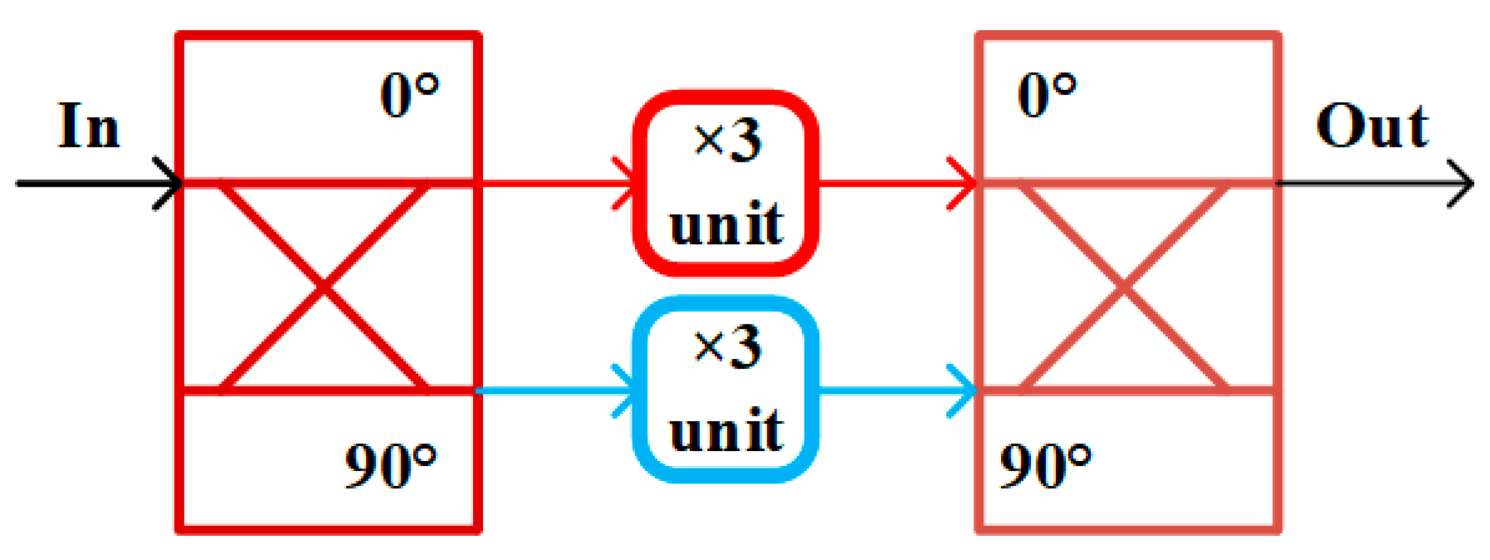
The balanced tripler depicted in Figure 2 consists of a fundamental-wave coupler, tripling units, and a third-harmonic coupler [7]. This configuration effectively suppresses the fundamental component and facilitates the extraction of the third harmonic.
In the design, the coupler splits the single-end input signal into two branches with a 90° phase difference. Each branch independently performs the frequency tripling, and their outputs are subsequently combined through the third-harmonic coupler to achieve efficient power summation.
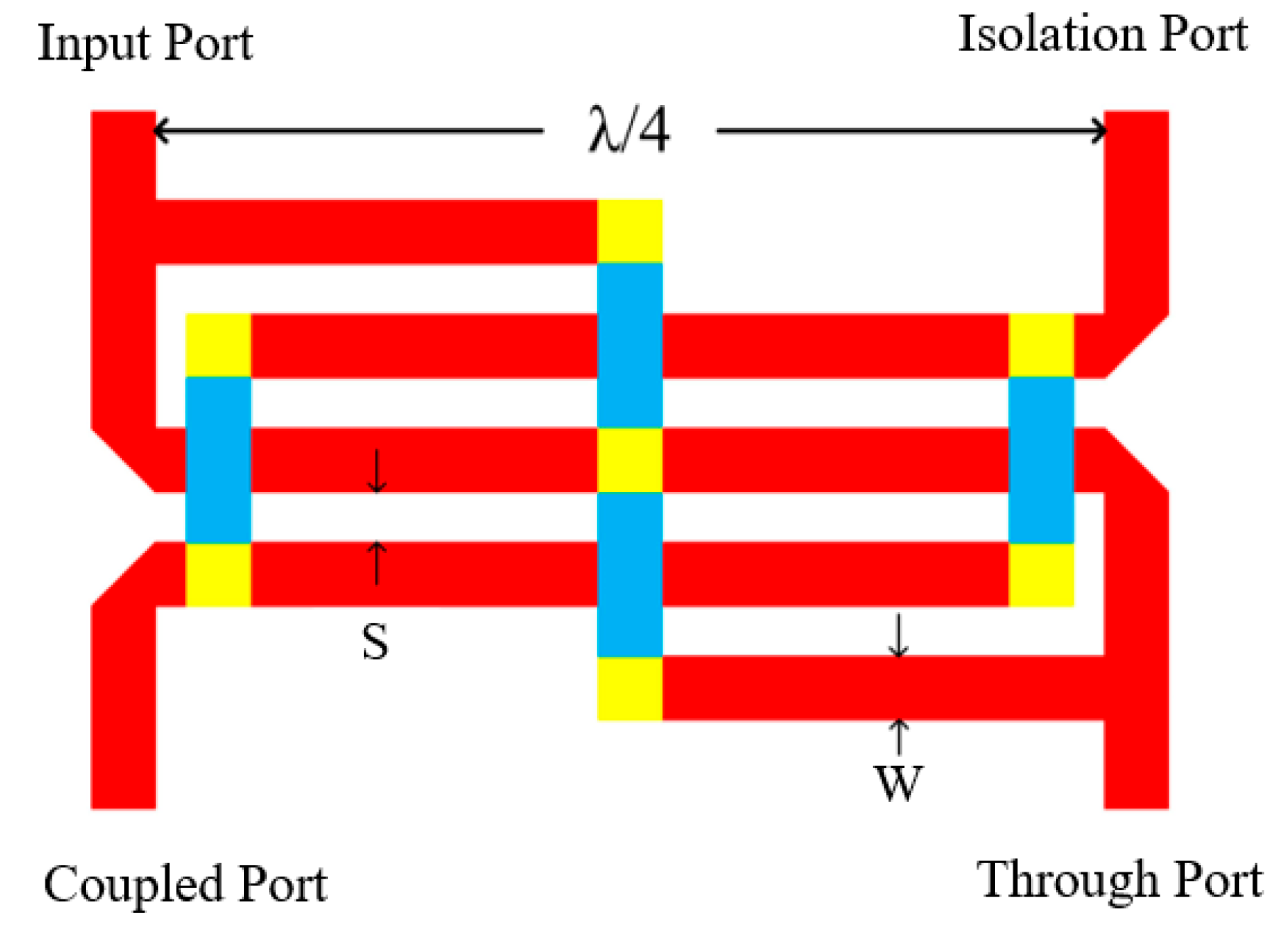
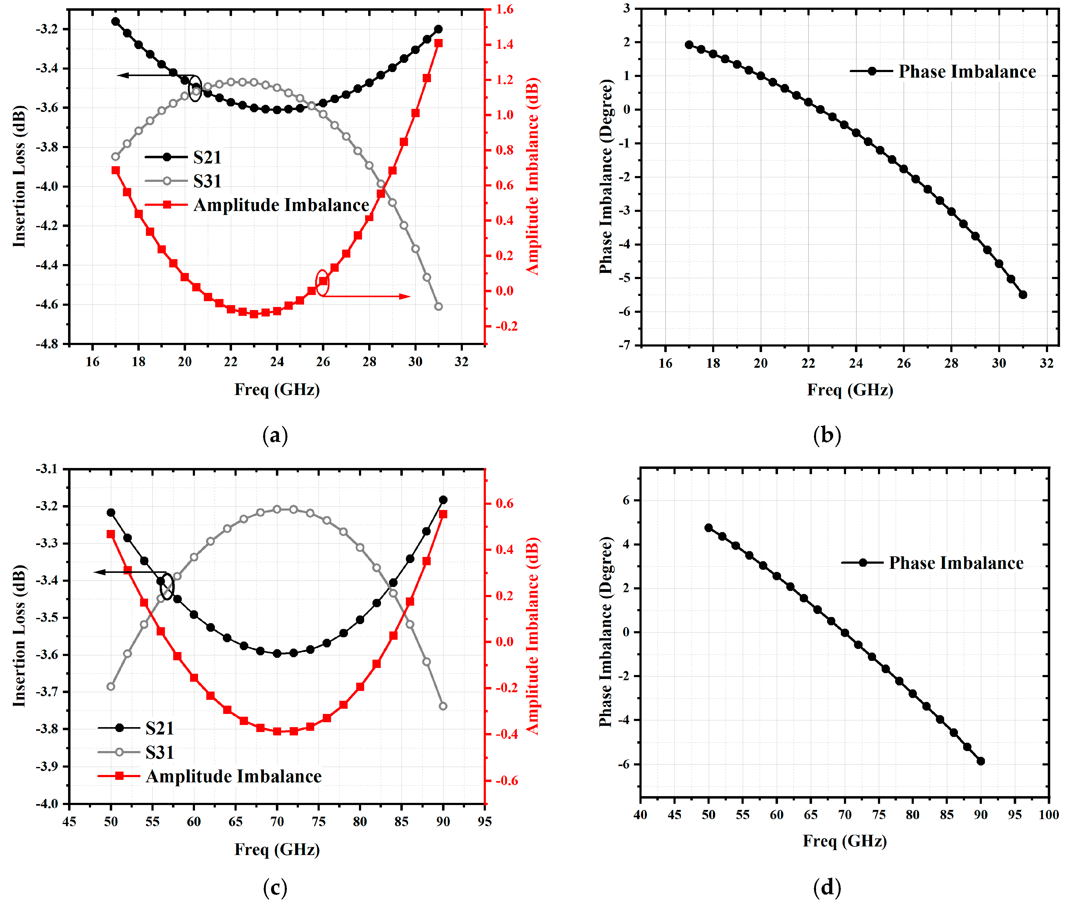
As shown in Figure 3, the Lange coupler is composed of several λ/4 transmission line sections. The simulated amplitude and phase imbalances of the two Lange couplers are shown in Figure 4. The amplitude and phase imbalances of the fundamental frequency coupler and the third-harmonic coupler are less than 0.13 dB and 1.5°; 0.4 dB and 4°, respectively.
The schematic of the tripler unit is shown in Figure 5, where Q1 serves as a driver amplifier to provide sufficient input power, enabling the tripler transistor Q2 to achieve a high third-harmonic conversion gain. Q2 generates the third harmonic, which is biased in Class A mode to suppress the second harmonics. R1 and R4 are connected in series with the transistor gates to reduce the conversion gain and improve low-frequency stability.
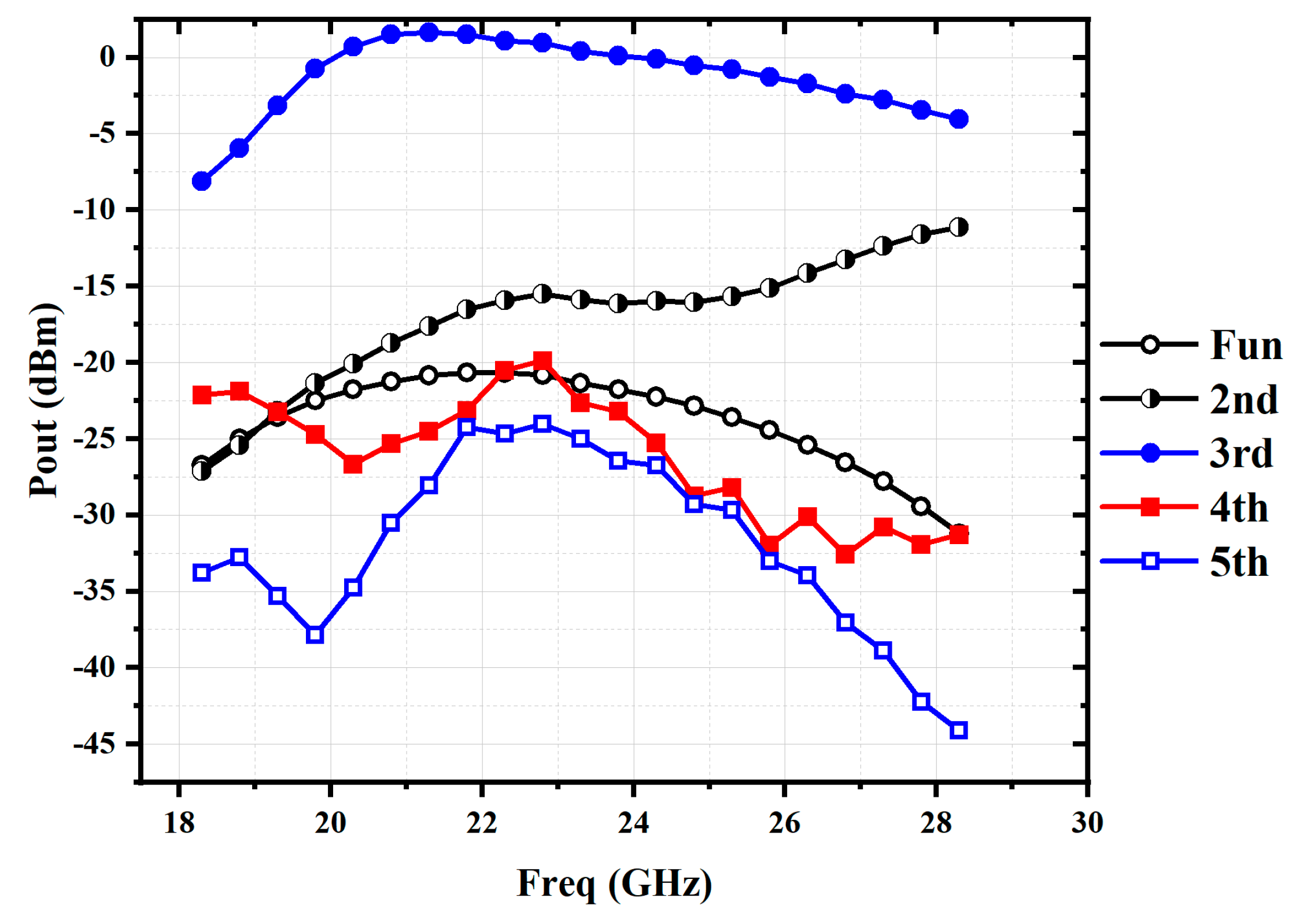
The output power versus the frequency of the proposed balanced tripler is simulated with an input power level of 0 dBm, and the results are shown in Figure 6. The fundamental power is suppressed by more than 20 dBc, and the second harmonic can be further attenuated through post-stage circuit.

2.2. Design of the Inter-Stage E-Band PA

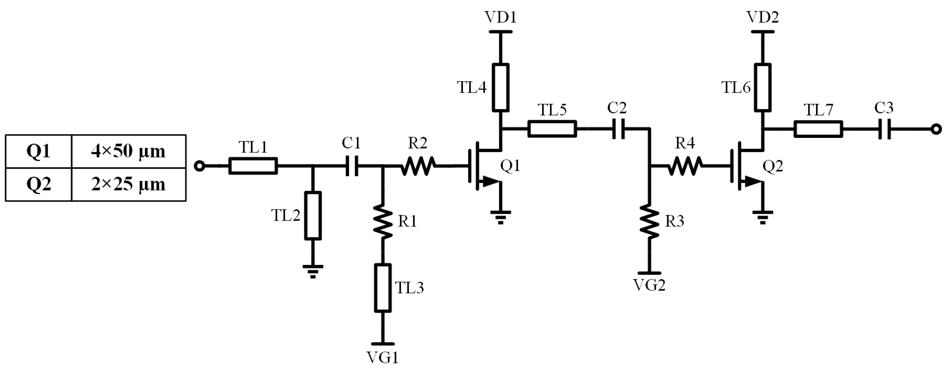
An inter-stage power amplifier is designed to amplify the third-harmonic output of the preceding tripler stage and to provide sufficient drive power for the subsequent passive frequency doubler, as well as adding extra rejection to other unwanted harmonic outputs. This ensures enhanced second-harmonic conversion gain at the output of the doubler. Similar to the tripler, R2 is serially connected to the gate to improve the stability of the PA. The schematic diagram of the designed power amplifier is presented in Figure 7.
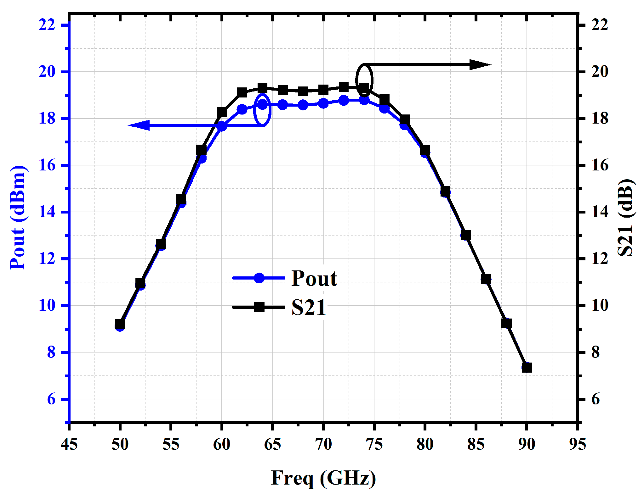
As shown in Figure 8, the small-signal gain S21 exceeds 19 dB, with a 3 dB bandwidth ranging from 57.7 to 80.3 GHz. Under a 0 dBm input power, the output power exceeds 18 dBm, corresponding to a large-signal gain greater than 18 dB, with a bandwidth extending from 57.2 to 81.1 GHz.
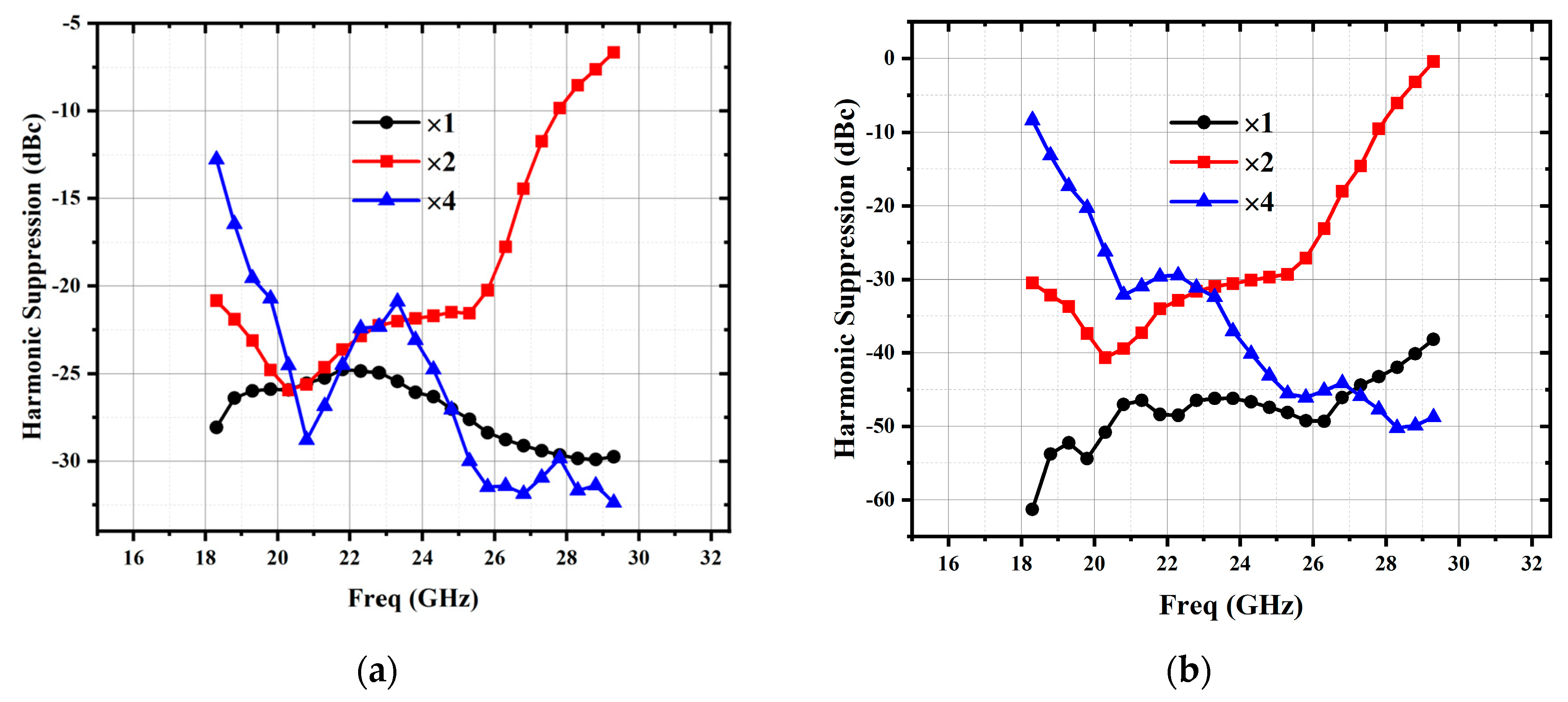
To further suppress the harmonics generated by the preceding tripler stage, the PA matching circuit is designed as a band-pass frequency-selective network. This network is composed of capacitors and microstrip lines, which simultaneously serves the dual purpose of impedance matching and harmonic rejection. As shown in Figure 9, a significant improvement in the suppression of the fundamental, second-order harmonic, and fourth-order harmonic is observed after the PA, from −21.2~−32.5 dBc to −29.6~−50.7 dBc for input frequency of 21.05~25.45 GHz.

2.3. Design of the Single-Balanced D-Band Doubler

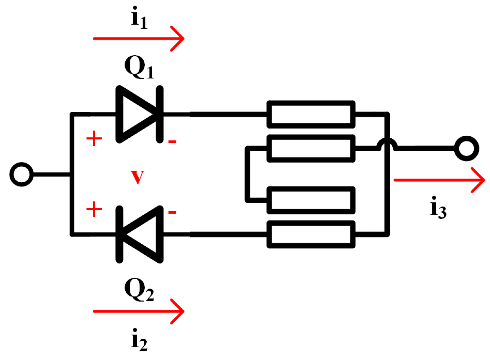
The designed single-balanced doubler consisting of a pair of anti-parallel diodes and a Marchand balun is shown in Figure 10. This architecture effectively utilizes the nonlinear characteristics of diodes to achieve frequency doubling, while suppressing the odd-order harmonics and extracting even-order harmonics [5].
In the single-balanced doubler, the anti-parallel diodes, which are realized using two discrete diode elements, require input signals of equal amplitude and in-phase relationship to effectively cancel the odd-order harmonics. However, because one diode is driven at the anode and the other at the cathode, this inevitably introduces asymmetry in both the physical structure and the output impedance. The asymmetrical Marchand balun is employed to compensate for this imbalance. The layout is shown in Figure 11; two unequal-length coupled-line sections are utilized for this compensation. All the design parameters are optimized with Advanced Design System.
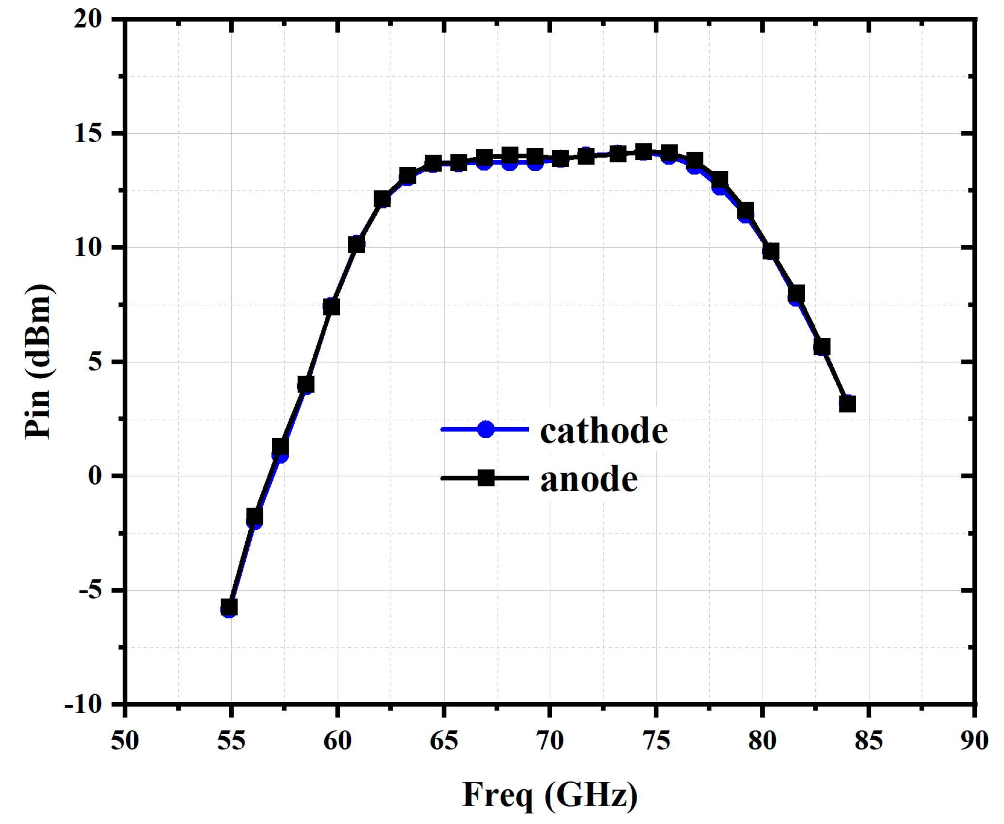
As shown in Figure 12, with this asymmetrical Marchand balun, the two anti-parallel diodes receive equal input power, approximately 14 dBm. In total, the single-balanced doubler obtains an input power of 17 dBm from the PA. All the large-signal simulations were conducted using the harmonic balance with Advanced Design System.

3. Measured Results

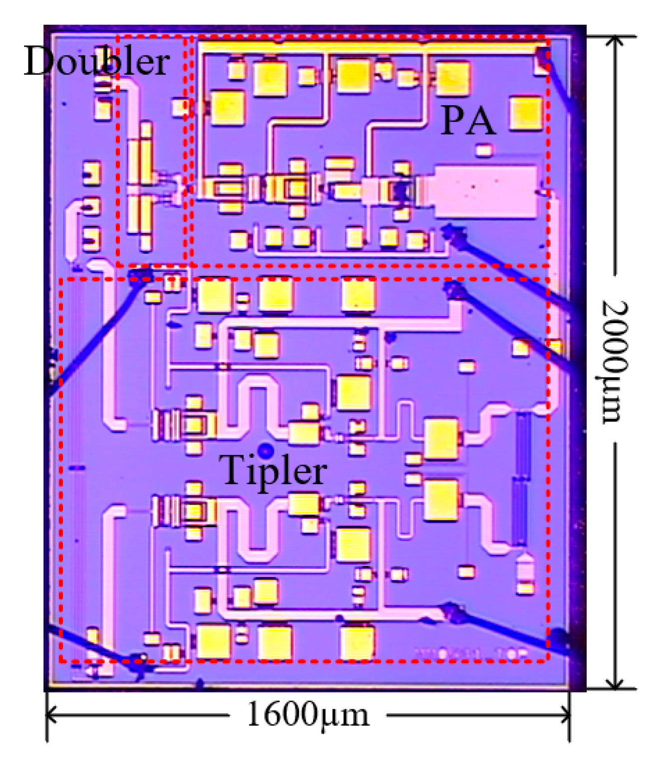
Figure 13 shows a microphotograph of the proposed six-times frequency multiplication chain. The chip occupies a total area of 1600 μm × 2000 μm, including all pads. The circuit is measured using on-wafer probing at room temperature (~26 D.C.). S11 and S22 are measured with GGB probe Model 50A-GSG and Cascade probe I170-T-GSG, using a vector network analyzer (Keysight N5245A) and with VNA extenders (OML V06VNA2-T/R-A_RLA 110-170G), respectively, using SOLT calibration sets. In large-signal measurements, the input signal is provided by a signal generator (R&S SMW200A), while the output power is recorded by an Erickson PM4 power meter and spectrum analyzer (Keysight N9030A) with D-band mixer SFB-06-N1.
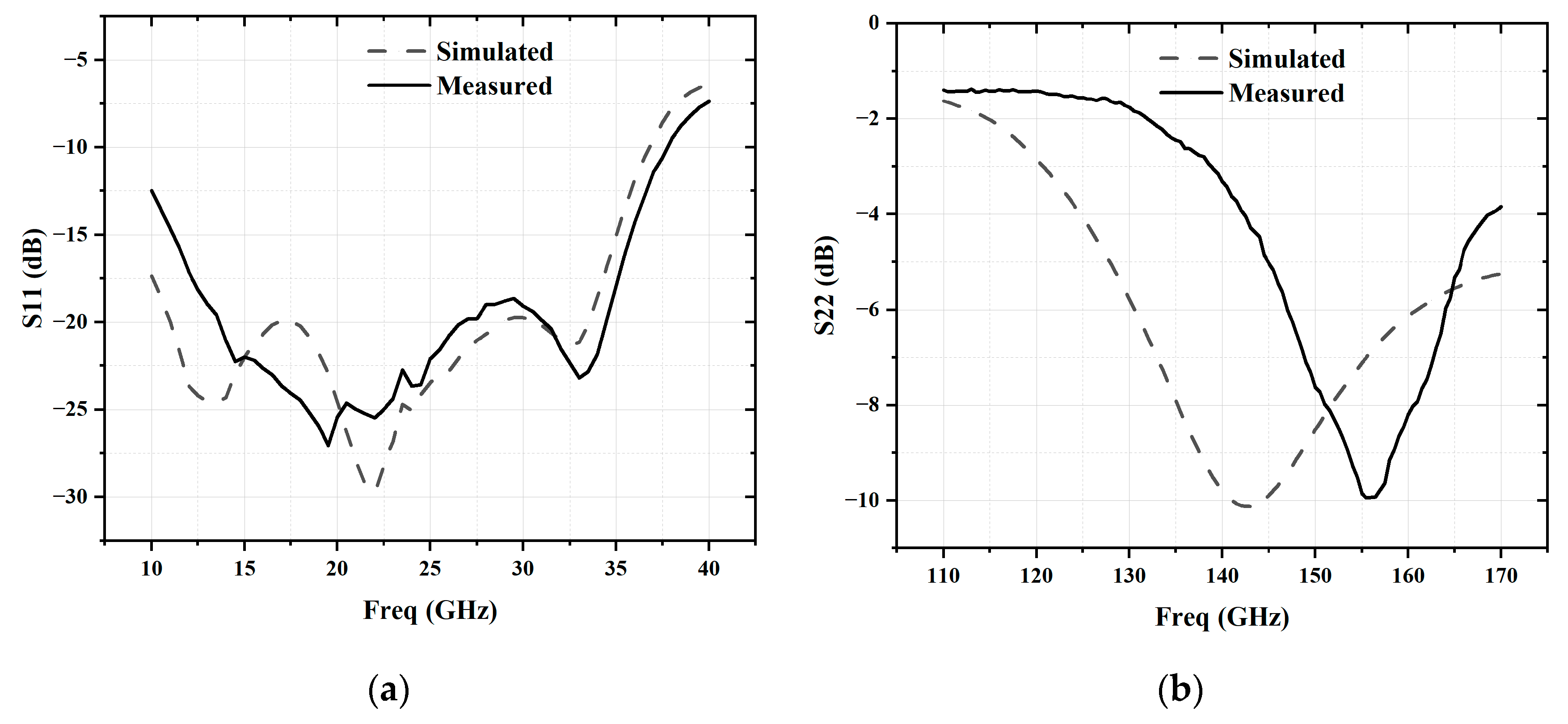
As shown in Figure 14, the measured S11 coincides well with the simulation, remaining below −10 dB across the 10 to 37 GHz frequency range. However, the measured S22 deviates from the simulation, shifting by 13.5 GHz towards higher frequencies. This deviation may be attributed to the fact that the device models in the PDK used in this work are not based on measured data above 90 GHz, but rather derived from curve fitting, which may not be entirely accurate. Meanwhile, the utilized ADS EM simulation tool may also introduce simulation inaccuracies in D-band. And the transistors’ metal figures are added in the EM simulation, which may overestimate the parasitic effects for the passive circuits, leading to a frequency shift in measurement.
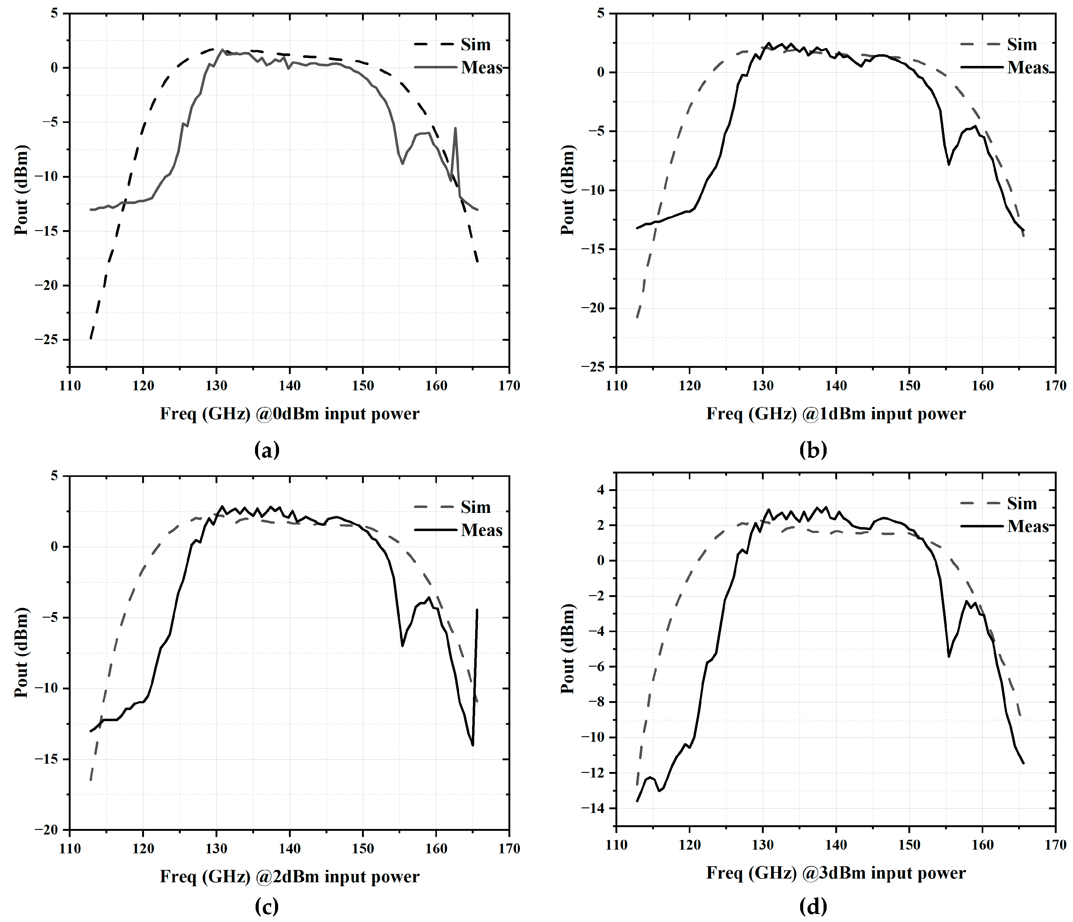
Figure 15 shows a comparison between the measured and simulated output power of the frequency sextupler chain under input power levels of 0 dBm, 1 dBm, 2 dBm, and 3 dBm. The measured saturated output power is 3.04 dBm, corresponding to an input power of 3 dBm. At an input power of 1 dBm, the peak output power reaches 2.14 dBm, resulting in a conversion gain of 1.14 dB. The 3 dB output bandwidth spans from 126.9 to 151.8 GHz, giving a relative bandwidth of 17.9%. At an input power of 2 dBm, the peak output power is 2.33 dBm, with a conversion gain of 0.33 dB and an output bandwidth of 3 dB ranging from 126.3 to 152.7 GHz, corresponding to a relative bandwidth of 18.9%.
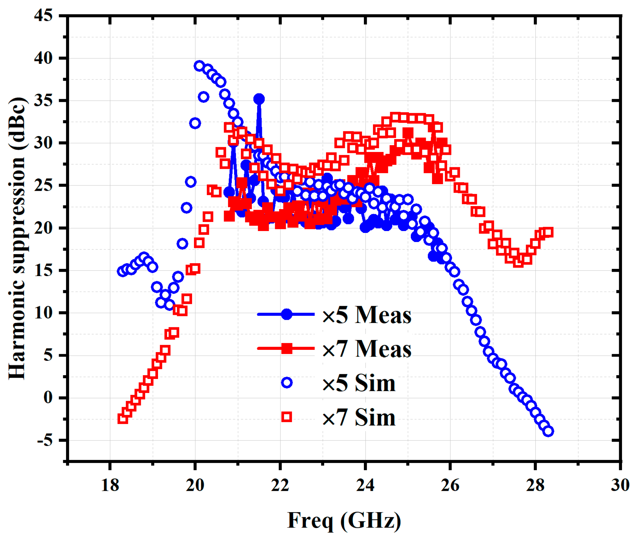
Figure 16 shows the simulated and measured 5th and 7th harmonic suppression of the frequency sextupler chain at an input power of 2 dBm. The measured results show that within the 3 dB output bandwidth of 126.3–152.7 GHz, both the 5th and 7th harmonics are suppressed by more than 20 dBc. Table 1 compares this work with other reported multiplier designs in GaAs process, where this work shows the widest 3 dB output frequency bandwidth in D-band with high harmonic rejections.

4. Conclusions

In this paper, the design of a D-band frequency sextupler chain is presented in a 100 nm GaAs pHEMT process. The presented circuit consists of balanced tripler, harmonic-rejection PA and output doubler. At an input power of 2 dBm, the peak output power of the sextupler reaches 2.33 dBm, resulting in a conversion gain of 0.33 dB. The 3 dB output bandwidth spans from 126.3 to 152.7 GHz, corresponding to a relative bandwidth of 18.9%. Moreover, the 5th and 7th harmonics suppression are better than 20 dBc across the operating frequency range, making it suitable for the wideband signal generation in D-band applications.

Author Contributions

Conceptualization, P.W.; Writing original draft preparation, P.W.; Conceptualization, Z.C.; Validation, Z.C.; Supervision, Z.C.; Methodology, Y.G.; Formal analysis, Y.G.; Methodology, Y.Q.; Software, Y.Q.; Data curation, P.Y.; Resources, P.Y.; Writing—review and editing, Z.C. and P.W. All authors have read and agreed to the published version of the manuscript.

Funding

This work was funded in part by the National Natural Science Foundation of China under Grant 62171128 and Grant 62188102, in part by the Top-Ten Technological Projects for Hunan Province in 2025 under Grant 2025QK1009, and in part by the Fundamental Research Funds for the Central Universities under Grant 2242022k60008.

Data Availability Statement

The original contributions presented in the study are included in the article, further inquiries can be directed to the corresponding author.

Conflicts of Interest

The authors declare no conflicts of interest.

References

  1. Zhou, P.; Chen, J.; Yan, P.; Yu, J.; Hu, J.; Dong, H.; Wang, L.; Hou, D.; Gao, H.; Hong, W. A 28.5-dB EVM 64-QAM 45-GHz Transceiver for IEEE 802.11aj. IEEE J. Solid State Circuits 2021, 56, 3077–3093. [Google Scholar] [CrossRef]
  2. Rappaport, T.S.; Xing, Y.; Kanhere, O.; Ju, S.; Madanayake, A.; Mandal, S.; Alkhateeb, A.; Trichopoulos, G.C. Wireless Communications and Applications Above 100 GHz: Opportunities and Challenges for 6G and Beyond. IEEE Access 2019, 7, 78729–78757. [Google Scholar] [CrossRef]
  3. Li, C.; Liu, P.; Zhu, X.W.; Zhu, A. A SIW-based Wideband Circularly Polarized 4 × 4 Patch Array Antenna in 45 GHz Band. In Proceedings of the 2019 12th UK-Europe-China Workshop on Millimeter Waves and Terahertz Technologies (UCMMT), London, UK, 20–22 August 2019; pp. 1–4. [Google Scholar]
  4. Wang, L.; Chen, J.; Hou, D.; Hong, W. A 45 GHz Low-Voltage Cascode Power Amplifier Based on Capacitor Coupling Technology. In Proceedings of the 2021 IEEE MTT-S International Wireless Symposium (IWS), Nanjing, China, 23–26 May 2021; pp. 1–3. [Google Scholar]
  5. Zhu, F.; Luo, G. A W-Band Frequency Quadrupler MMIC. In Proceedings of the 2020 International Conference on Microwave and Millimeter Wave Technology (ICMMT), Shanghai, China, 20–23 September 2020; pp. 1–3. [Google Scholar]
  6. Chandra-Prabhu, A.; Grzyb, J.; Hillger, P.; Heinemann, B.; Rücker, H.; Pfeiffer, U. A Wideband W-Band Frequency Tripler with a Novel Mode-Selective Filter for High Harmonic Rejection. In Proceedings of the 2023 18th European Microwave Integrated Circuits Conference (EuMIC), Berlin, Germany, 18–19 September 2023; pp. 197–200. [Google Scholar]
  7. Kallfass, I.; Tessmann, A.; Massler, H.; Lewark, U.; Kuri, M.; Riessle, M.; Zink, M.; Leuther, A. Balanced active frequency multipliers for W-band signal sources. In Proceedings of the 2011 6th European Microwave Integrated Circuit Conference, Manchester, UK, 10–12 October 2011; pp. 101–104. [Google Scholar]
  8. Hu, Y.; Xie, J.; Bi, X. A W-band Frequency Tripler with 8-dBm Output Power Using 0.25-m GaAs pHEMT Process. In Proceedings of the 2022 IEEE MTT-S International Microwave Workshop Series on Advanced Materials and Processes for RF and THz Applications (IMWS-AMP), Guangzhou, China, 12–14 December 2022; pp. 1–3. [Google Scholar]
  9. Kim, M.; Choi, K.; Kim, J. W -Band Backward Distributed Frequency Doubler Using GaAs 0.15-µm pHEMT Process. IEEE Microw. Wirel. Compon. Lett. 2019, 29, 400–402. [Google Scholar] [CrossRef]
  10. Ye, Y.; Zhang, J.; Sun, X.W. A W-Band Traveling-Wave Frequency Doubler With Output Power of 9 dBm and Power Efficiency of 11.2%. IEEE Microw. Wirel. Compon. Lett. 2014, 24, 704–706. [Google Scholar] [CrossRef]
  11. Campos-Roca, Y.; Verweyen, L.; Fernandez-Barciela, M.; Bischof, W.; Curras-Francos, M.; Sanchez, E.; Hulsmann, A.; Schlechtweg, M. 38/76 GHz PHEMT MMIC balanced frequency doublers in coplanar technology. IEEE Microw. Guid. Wave Lett. 2000, 10, 484–486. [Google Scholar] [CrossRef]
  12. Lu, K.H.; Huang, J.J.; Chen, W.C.; Chang, H.Y.; Wang, Y.C. A K-Band Frequency Doubler in 0.15-µm GaAs pHEMT with an Autonomous Circuit for Stability Analysis. In Proceedings of the 2018 IEEE International Symposium on Radio-Frequency Integration Technology (RFIT), Melbourne, Australia, 15–17 August 2018; pp. 1–3. [Google Scholar]
  13. Shi, Q.H.; Liu, W.L.; Lu, Y.; Liu, X.; Feng, T.; Zhao, Z.Y.; Yi, C.P.; Ma, X.H.; Hao, Y. An E/W-band Frequency Doubler with 10.5-dBm Output Power Using 0.1-m GaAs pHEMT Process. In Proceedings of the 2024 IEEE MTT-S International Microwave Workshop Series on Advanced Materials and Processes for RF and THz Applications (IMWS-AMP), Nanjing, China, 9–11 November 2024; pp. 1–3. [Google Scholar]
Figure 1. Architecture diagram of the frequency sextupler chain.
Micromachines 16 00984 g001
Figure 2. Architecture diagram of the balanced tripler.
Micromachines 16 00984 g002
Figure 3. Layout of Lange coupler.
Micromachines 16 00984 g003
Figure 4. Simulated amplitude and phase imbalance of two Lange couplers: (a) amplitude imbalance of fundamental-wave coupler; (b) phase imbalance of fundamental-wave coupler; (c) amplitude imbalance of third-harmonic coupler; (d) phase imbalance of third-harmonic coupler.
Micromachines 16 00984 g004
Figure 5. Schematic of tripler unit.
Micromachines 16 00984 g005
Figure 6. Simulated output power of the balanced tripler with an input level of 0 dBm.
Micromachines 16 00984 g006
Figure 7. Schematic of PA.
Micromachines 16 00984 g007
Figure 8. Simulated small-signal gain and large-signal gain of PA.
Micromachines 16 00984 g008
Figure 9. Harmonic suppression of PA: (a) harmonic suppression without PA; (b) harmonic suppression with PA.
Micromachines 16 00984 g009
Figure 10. Schematic of single-balanced doubler.
Micromachines 16 00984 g010
Figure 11. Layout of the asymmetrical Marchand balun.
Micromachines 16 00984 g011
Figure 12. Simulated input power of the single-balanced doubler.
Micromachines 16 00984 g012
Figure 13. The microphotograph of six-times frequency multiplication chain.
Micromachines 16 00984 g013
Figure 14. Simulated and measured S-parameters: (a) S11; (b) S22.
Micromachines 16 00984 g014
Figure 15. Simulated and measured large-signal versus input power: (a) output power @0dBm input power; (b) output power @1dBm input power; (c) output power @2dBm input power; (d) output power @3dBm input power.
Micromachines 16 00984 g015
Figure 16. Simulated and measured harmonic suppression.
Micromachines 16 00984 g016
Table 1. Comparison with other reported GaAs multiplier designs.
Reference[7][8][9][10][11][12][13]This Work
Process100 nm250 nm150 nm100 nm150 nm150 nm100 nm100 nm
AlGaAsGaAsGaAsGaAsGaAsGaAsGaAsGaAs
mHEMTpHEMTpHEMTpHEMTpHEMTpHEMTpHEMTpHEMT
Freq (GHz)79–10090–9988–99.585–11034.44–42.5637–4371–90126.3–152.7
Multi Factor83222226
Gain (dB)8.9−3−4.33.2−40.9−3.30.33
Pout (dBm)6.987.18.280.910.52.33
Size (mm2)62.2121.35NA0.721.93.2
Disclaimer/Publisher’s Note: The statements, opinions and data contained in all publications are solely those of the individual author(s) and contributor(s) and not of MDPI and/or the editor(s). MDPI and/or the editor(s) disclaim responsibility for any injury to people or property resulting from any ideas, methods, instructions or products referred to in the content.