2.1. Device Fabrication
First, the substrate with a self-contained 285 nm thick SiO2 insulating layer was ultrasonically cleaned for 10 min each in acetone, alcohol, and deionized water to remove impurities on the substrate surface. Then, it was blown dry with nitrogen, homogenized using a coater, and dried on a dryer for 5 min. A lithography was performed using a mask and American ABM Company Ultraviolet lithography machine, and it was dried again on a dryer for 5 min. Place the sample on the photolithography machine and expose it naked for 3 s. After completion, put the sample into sodium hydroxide solution and then pure water. Repeat this step for development. After drying, observe it under a microscope. Secondly, AZTO films were deposited byPVD75 Magnetron Sputtering System by Kurt J. Lesker, USA. Then, they were washed with acetone, alcohol, and deionized water for 3 min each, and dried with nitrogen. The samples were placed in German-made RTP-100 rapid thermal processor for annealing. After annealing was completed, secondary photolithography was carried out using a mask and a photolithography machine. After photolithography was completed, the samples were placed in sodium hydroxide solution and then pure water for secondary development. After the development was completed, it was dried with nitrogen gas. Finally, the sample was placed in LN-2063SA organic vapor deposition system manufactured by Shenyang Lining Vacuum Technology Research Institute, Chinato prepare the Al electrode. At this point, the AZTO artificial synaptic device has been successfully fabricated.
2.2. Device Structure and Characterization
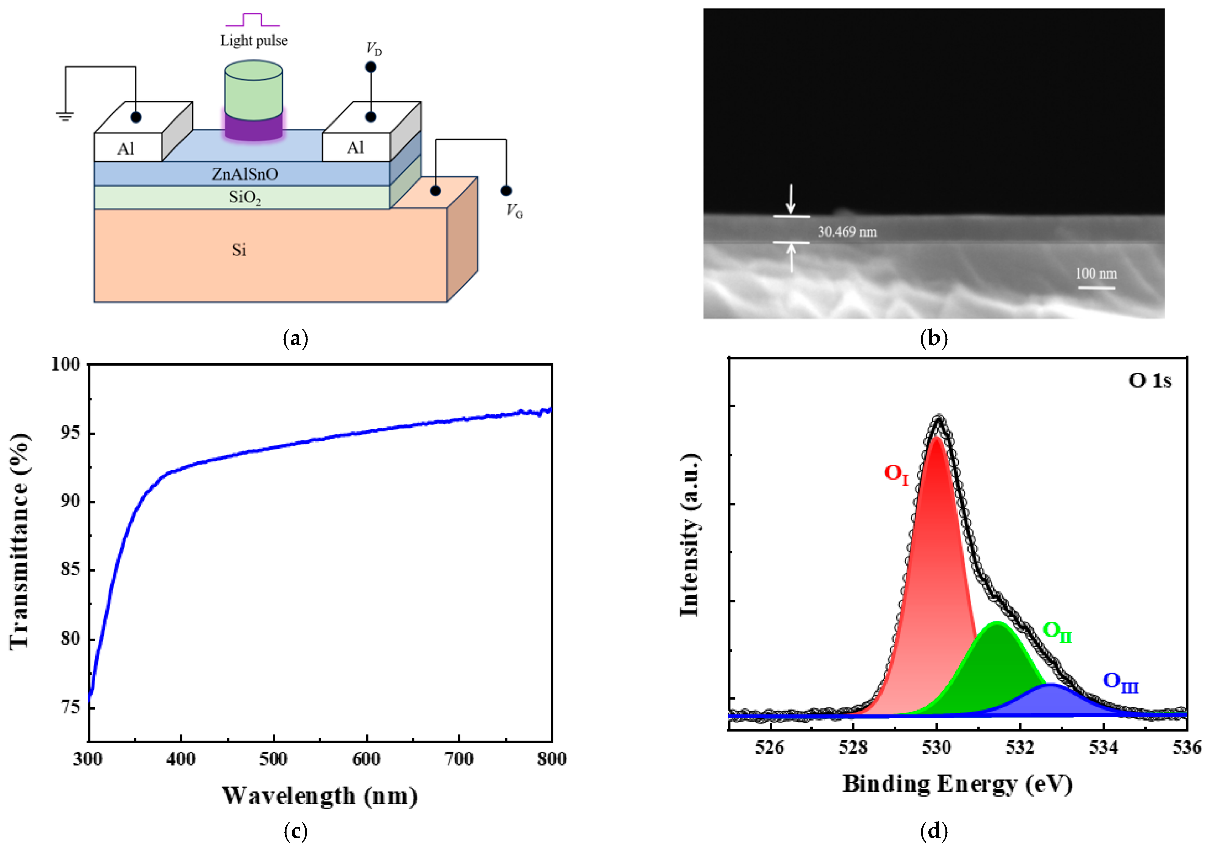
The structure of the AZTO artificial synaptic device is shown in
Figure 1a. The thickness of the AZTO film was measured to be approximately 30 nm using a scanning electron microscope, as shown in
Figure 1b. The transmittance of the film was tested using a Shimadzu UV-2600 UV-Vis spectrophotometer, as shown in
Figure 1c.
Figure 1d shows the XPS spectrum of O-1s. The spectrum of O-1s is divided into three peaks, located at 529.99 eV (O
I), 531.44 eV (O
II), and 532.76 eV (O
III), representing lattice oxygen, oxygen vacancies, and adsorbed oxygen on the surface, respectively. Their respective contents are 61.77%, 30.29%, and 7.94%.
Figure 1e displays the XPS spectra of Al 2p, Zn 2p, Sn 3d, and full XPS spectra. The contents of C 1s, Al 2p, Zn 2p, Sn 3d, and O 1s are 31.75%, 0.75%, 20.21%, 11.92%, and 35.38%, respectively.
Figure 1d and e were tested using the ESCALAB 250Xi equipment manufactured by Thermo Fisher Scientific.
Figure 1f presents the AFM image of AZTO. It was tested using an MFP-3D atomic force microscope manufactured by Oxford Instruments in the UK. The surface area of the film selected for testing was 5 μm × 5 μm. The surface morphology of the film was tested using atomic force microscopy (AFM), and the film surface was found to be uniform overall. The roughness measured by AFM was 161.46 pm, indicating that the film surface was relatively flat.
Figure 1g shows the XRD test results for the sample, revealing no diffraction peaks in the fabricated device. This indicates that the AZTO film exhibits an amorphous structure and that AZTO exists in an amorphous state.
Figure 1g was tested using a D8 DISCOVER X-ray diffractometer manufactured by Bruker Corporation of Germany.
2.3. The Electrical Properties of AZTO-TFT
The electrical properties of AZTO-TFT were analyzed and tested using a semiconductor parameter meter.
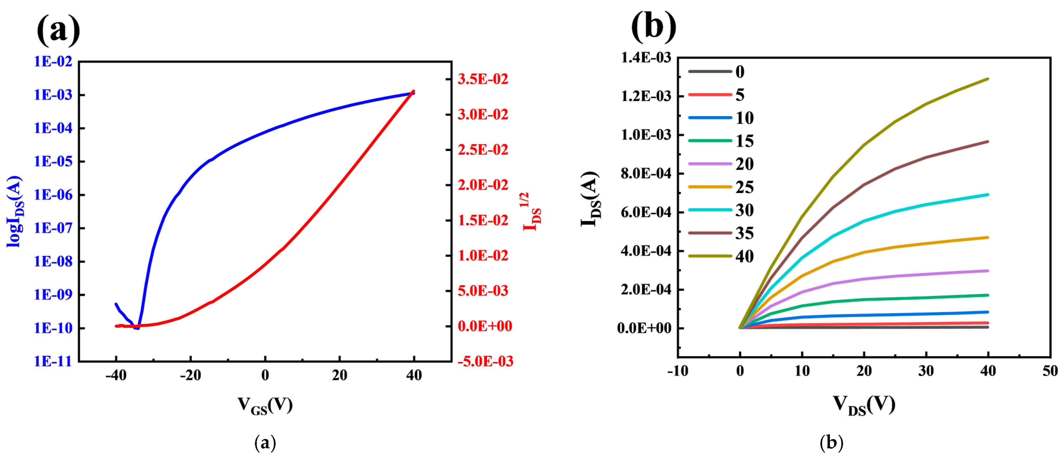
Figure 2a shows the transfer characteristic curve of AZTO-TFT. The transfer characteristic curve is a graph showing the relationship between the channel current and the gate voltage. When testing the transfer characteristic curve, the variation range of the gate voltage was −40–40 V. The drain voltage is 20 V.
Figure 2b shows the output characteristic curve of AZTO-TFT. The output characteristic curve is the relationship graph of the channel current varying with the drain voltage. When testing the output characteristic curve, the conditions of the channel current varying with the drain voltage under the gate voltage in nine cases were tested, respectively. The variation range of the gate voltage was 0–40 V, with a step size of 5 V. The variation range of the drain voltage was 0–40 V.
The principle behind the transfer characteristic curve of a TFT is that a conductive channel is induced in the active layer by the gate voltage. When
VGS exceeds the threshold voltage, a conductive channel forms in the active layer, and
IDS increases with increasing
VGS. As
VGS continues to increase,
IDS approaches saturation. As shown in
Figure 2a, as the gate voltage increases,
IDS increases rapidly, and the device exhibits excellent switching characteristics. It can be seen from
Figure 2b that when the gate voltage is higher than the threshold voltage, the channel current first shows a linear increasing trend with the increase of
VDS. As V
D continues to increase, the channel current tends to saturation, meaning that the channel current no longer increases with the increase of V
DS.
Combined with the characteristic curve of the thin-film transistor, the off-state current, on-state current, switching ratio, sub-threshold swing, carrier mobility, and threshold voltage of the device can be calculated according to Equations (1)–(3).
In the equation, Ci represents the area capacitance of the gate insulation layer, W is the channel width of the active layer, L is the channel length of the active layer, VGS indicates the voltage applied to the gate, and IDS is the channel current.
It can be known through calculation that the current-switching ratio of the device is 1.18 × 10⁷, the subthreshold swing is 1.48 V/decade, the mobility is 2.51 cm2V−1s−1, and the threshold voltage is −9.40 V.
2.4. Synaptic Characteristic Simulation
The human brain is a highly complex network composed of a large number of neurons [
27,
28,
29]. Numerous neurons are connected to other neurons through synapses, and neuron cells are composed of dendrites, cell bodies, and axons. The axon terminals of neurons have many tiny branches. The swollen part at the end of each branch is the synaptic vesicle. The synaptic vesicle of the previous neuron is connected to the cell body or dendrite of the next neuron to form a synapse. The connection strength between neurons is called synaptic weight. Synaptic plasticity refers to the property that the connection strength between neurons can be regulated. Synapses consist of three parts: the presynaptic membrane, the synaptic cleft, and the postsynaptic membrane. The axon terminals contain many synaptic vesicles. When the brain is stimulated by signals, the synaptic vesicles are stimulated and fuse with the presynaptic membrane, releasing neurotransmitters (converting electrical signals into chemical signals). Neurotransmitters then bind to receptors on the postsynaptic membrane through the synaptic cleft (converting chemical signals into electrical signals). It triggers potential changes in the postsynaptic membrane. After the signal transmission is completed, the neurotransmitter separates from the receptor.
The bandgap refers to the energy difference between the lowest point of the conduction band and the highest point of the valence band. The energy of incident light must exceed the semiconductor’s bandgap to excite electron transitions. Ultraviolet light has shorter wavelengths and higher energy than visible light. Materials with larger bandgaps typically absorb ultraviolet light because its high energy is sufficient to enable electrons to jump across the bandgap into higher energy levels. When ultraviolet light is incident on a device, electrons in the valence band absorb the energy of incident photons and transition to the conduction band. The fundamental principle and mechanism underlying synapse characteristic simulation is essentially the persistent photoconductive effect in semiconductor materials. As a wide-bandgap semiconductor material, AZTO possesses the ability to absorb ultraviolet light, excite electron transitions, and generate a persistent photoconductive effect, making it suitable as the active layer for synapse devices.
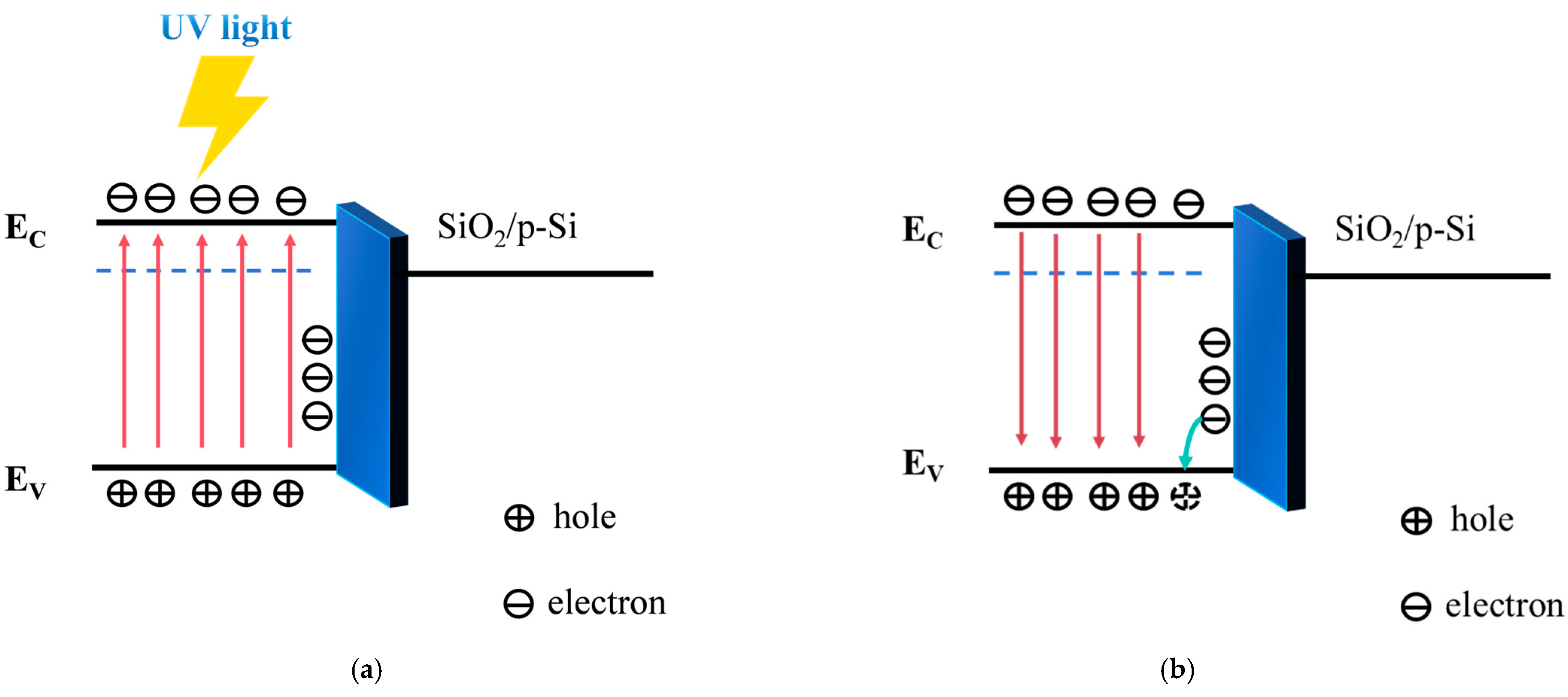
Figure 3 illustrates the band structure diagram under and after ultraviolet irradiation. After electron transitions occur, vacancies are left in the valence band. These vacancies are photogenerated holes, and photogenerated carriers are electron–hole pairs composed of photogenerated electrons and photogenerated holes. XPS tests have shown the existence of oxygen vacancies in AZTO. During the illumination process, Oxygen vacancies will capture photogenerated holes [
26,
30,
31]. Due to the capture effect of interface charges, some photogenerated electrons will accumulate at the interface, and another part will be replenished into the transistor’s conductive channel, thus increasing the conductivity. Due to the continuous photoconductive effect of semiconductors, even after the light pulse ends, the channel conductivity of the device will not change immediately. The above process can be explained according to Equations (4) and (5):
For three-terminal devices, the source/drain electrode corresponds to the presynaptic/postsynaptic membrane, the light pulse can be regarded as the action potential acting on the presynaptic, and the photogenerated electrons are equivalent to neurotransmitters. Then, the transistor channel current I
DS can be regarded as the excitatory postsynaptic current. The synaptic characteristics of thin-film transistors were tested using a semiconductor parameter meter. The gate voltage was set to 0 V and the source-drain voltage was set to 0.5 V. Use a 365 nm UV LED curing point light source to illuminate the device at an angle, focusing the point light source on the device channel. The distance between the light source and the sample is 2 cm. Then, use a UV radiometer connected to a UVALED-X3 probe to measure the light power density. After applying a light pulse with a duration of 0.5 s and an optical power density of 3.66 mW/cm
2, the channel current I
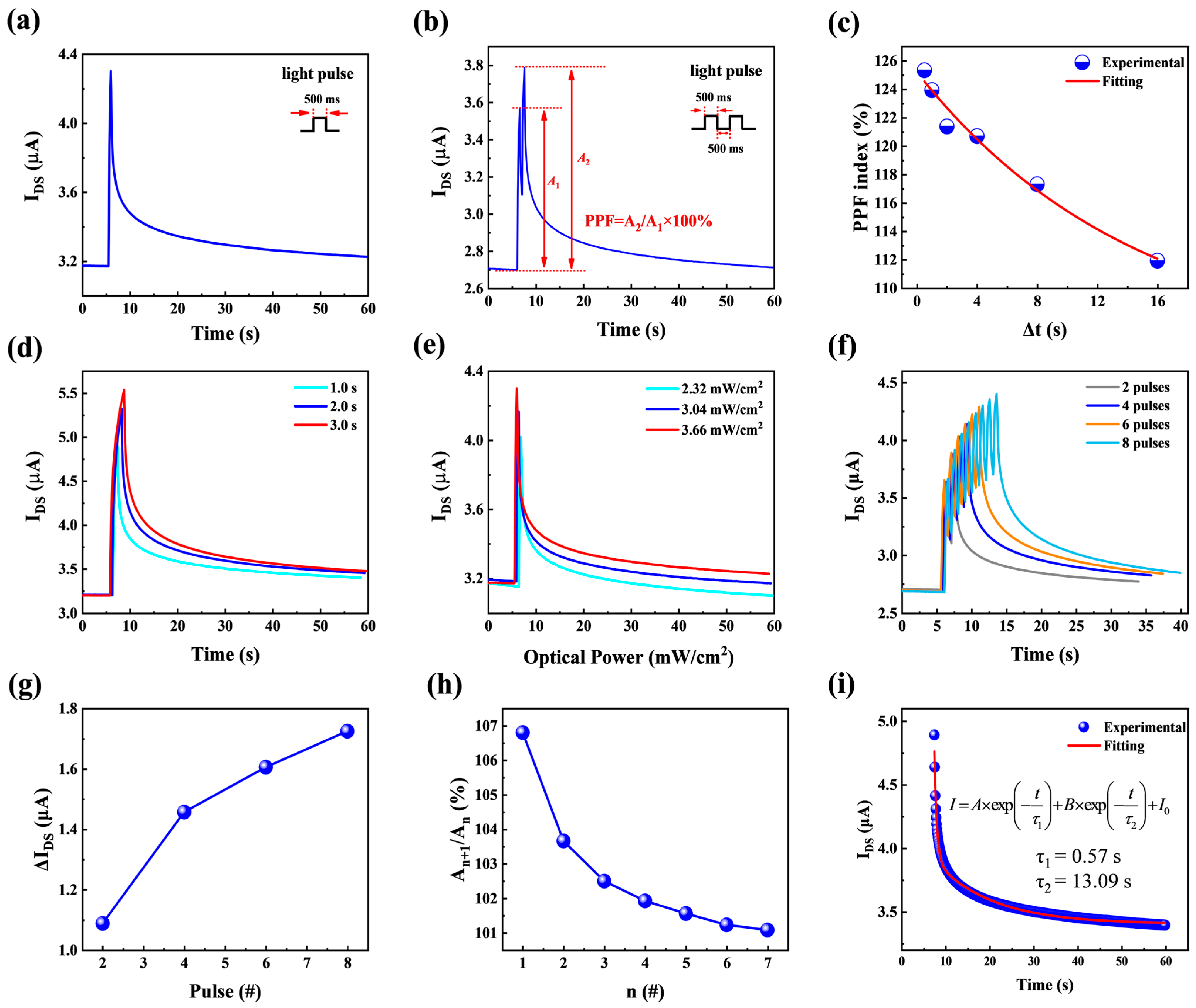
DS increased from 3.17 μA to 4.30 μA and gradually decreased after the end of the illumination, as shown in
Figure 4a. At the beginning, when there was no light pulse stimulation, the current was in the initial state and could be regarded as the resting state of the neuron. During the illumination process, the illumination leads to an increase in the carrier concentration, and the current rapidly increases to the peak, which can be regarded as the action state of the neuron. After the illumination ends, due to the continuous photoconductive effect, the current gradually decreases to the initial value, which can be regarded as the process of recovering from the action state to the resting state. The entire process is similar to EPSC in the short-term plasticity of the synapse. PPF refers to the phenomenon that if the presynaptic membrane is stimulated twice within a short time interval, the response of the postsynaptic membrane induced by the second stimulation is greater than that induced by the first stimulation. As can be seen from
Figure 4b, when the device is irradiated with two light pulses with an interval of 0.5 s, the current triggered by the second light pulse is greater than that triggered by the first light pulse. The reason is that after the first light pulse irradiates the device, photogenerated carriers are produced. Due to the continuous photoconductivity effect, it takes a certain amount of time for electrons and holes to return to their initial states. When the time interval between two optical pulses is less than the time required for the carriers to return to their initial state, the carrier concentration when the second optical pulse irradiates the device will be greater than that during the first optical pulse, thereby causing the second current response to be greater than the first current response. The PPF index can be calculated by Equation (6):
If the time interval between two optical pulses increases, more carriers will return to their initial state. That is to say, the difference in the amount of current change caused by the two optical pulses will decrease as the time interval increases. The experiment tested six groups of two-pulse generalization indices with time intervals of 0.5 s, 1 s, 2 s, 4 s, 8 s, and 16 s, respectively, and fitted them according to Equation (7):
The relationship between the PPF index and the time interval is shown in
Figure 4c. When the interval time is 0.5 s, the PPF index is 125.34%. With the increase in the pulse interval time, the PPF index shows a downward trend. As can be seen from
Figure 4c, the six groups of data have a high degree of fit with the fitted curve, which indicates that the PPF index shows an exponential downward trend with the increase in the pulse interval time. The entire process is similar to PPF in the short-term plasticity of synapses.
Figure 4d shows the relationship between the channel current and the duration of the light pulse. It can be seen from the figure that as the duration of light exposure increases, the peak value of the current becomes larger and larger, and the final value of the current decline after the same period of time following the peak value of the current is different. It can be known from the figure that the final value of the current increases with the increase in the duration of the light pulse. This is because when a longer duration of light pulse irradiates the device, the electrons in the valence band absorb more energy from the incident photons, generate more carriers, have a higher carrier concentration, and thus have a greater channel current. After the same descent time, the final value of the current is also greater. In other words, the longer the duration of the light pulse, the longer it takes for the current to drop to its initial value. In biology, synaptic weight refers to the connection strength between synapses. Synaptic plasticity is classified into short-term plasticity and long-term plasticity based on the duration of changes in synaptic connection strength. Excitatory postsynaptic current, as an important indicator of synaptic weight change [
32], can visually represent the change in synaptic weight. Therefore, the change in current with the light exposure time can indicate that synaptic plasticity also changes with the increase in light exposure time. The light pulse time is regarded as the learning time, and the decrease process of current after the disappearance of the light pulse is regarded as the forgetting process of memory. The magnitude of the current value reflects the level of memory. It can be understood more vividly that the synaptic weight has shown a tendency to transform from short-term plasticity to long-term plasticity. As the light exposure time increases from 1 s to 3 s, the transformation trend becomes more and more obvious.
Figure 4e shows the relationship between channel current and optical pulse power density. The principle is similar to that in
Figure 4d. It can be seen that as the optical power density increases, the current also increases, and after the same decline time, the final value of the current becomes larger.
Figure 4f shows the relationship between the channel current and the number of light pulses. The principle is similar to that in
Figure 4b. If the time interval between the previous light pulse and the next light pulse is less than the time required for the carriers to return to their initial state, it will result in the carrier concentration being greater when the device is illuminated by the next light pulse than when it is illuminated by the previous light pulse. This leads to the current increasing with the increase in the number of optical pulses.
Figure 4e,f are also simulations of the transformation process from short-term plasticity to long-term plasticity. It can be known from
Figure 4d–f that short-term plasticity can be transformed into long-term plasticity through methods such as reinforcement stimulation and continuous training.
Figure 4g shows the relationship between the change in current and the number of light pulses. The figure indicates that the change in current increases as the number of light pulses increases. As shown in
Figure 4h, the ratio of the current peaks triggered by adjacent pulses decreases gradually as the number of pulses increases. This is because the number of photoelectrons is limited, and the number of photoelectrons generated by subsequent light pulses decreases. This leads to a gradual decrease in the ratio of the current peaks triggered by adjacent pulses in
Figure 4h.
Figure 4i shows the attenuation curve of the current when the optical pulse time is 1 s, which is fitted using Equation (8):
After fitting with a double exponential decay function, the red line in the figure represents the fitted curve, where the parameters τ1 is 0.57 s and τ2 is 13.09 s. The time constants τ1 and τ2 correspond, respectively, to intrinsic shallow-level defects and deep-level defects within the active layer material of the device (τ1 corresponds to shallow-level defects, where carriers are readily captured, released, and participate in recombination processes; τ2 corresponds to deep-level defects, where captured carriers are difficult to release and function as recombination centers). The double-exponential decay of current is intrinsically linked to the material’s inherent defects, which govern carrier recombination pathways. Consequently, variations in τ1 and τ2 are closely tied to the material’s intrinsic properties rather than dependent on optical power, pulse width, or pulse count.
2.5. Simulation of EPSC and Logical Functions Under Different Gate Voltages
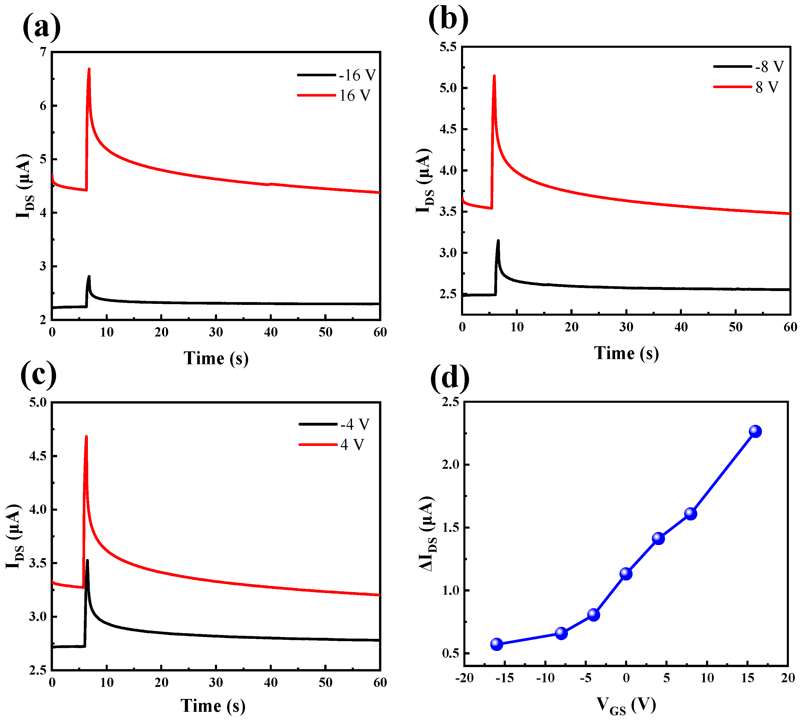
To test the influence of different gate voltages on EPSC, the gate voltage was changed, and the device was irradiated with a single optical pulse of an optical power density of 3.66 mW/cm
2 and a duration of 0.5 s. The EPSC under different gate voltages are shown in
Figure 5a–c.
Figure 5d shows the relationship between the variation in current and different gate voltages. When the gate voltage increases from −16 V to 16 V, ΔI
DS increases from 0.57 μA to 2.26 μA. It can be seen from the figure that the change in current increases with the increase in the gate voltage.
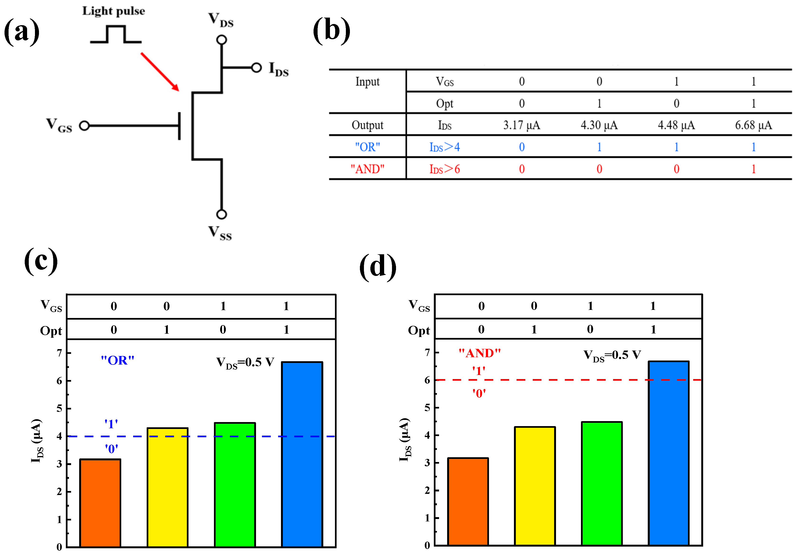
The gate voltage and the light pulse are regarded as two input signals, and the channel current value is regarded as the output signal. Based on the two sets of data of V
GS being 0 V and 16 V under the condition that the duration of the optical pulse is 0.5 s in the test, when V
GS is 0 V, it is defined as “0”; when V
GS is 16 V, it is defined as “1”; a pulse without light is defined as “0”; and a pulse with light is defined as “1”. The output of the device is jointly controlled by two input signals. When there is no input signal, the average value of the dark current is taken as the output. When the gate voltage is zero, the peak current caused by the optical pulse is taken as the output. When the gate voltage is 16 V and there is no light pulse input, the average value of the dark current is taken as the output. When the gate voltage is 16 V and there is an input of optical pulses, the peak value caused by the optical pulses is taken as the output. We can set 4 μA and 6 μA as current thresholds. As shown in
Figure 6b, this is the truth table of the logic gate of the device obtained through testing. The meaning of the “AND” logical operation state is the output is “1” only when all input signals are “1”; otherwise, it is “0”. The meaning of the “OR” logical operation state is as long as one input signal is “1”, the output will be “1”. Based on this principle, by introducing two types of input signals in thin-film transistors, two different logical operations, “AND” and “OR”, can be achieved. It is better than other optoelectronic synaptic devices shown in
Table 1. The logic operation diagrams of “OR” and “AND” are shown in
Figure 6c and d, respectively.
Among the information obtained by the human brain, the information transmitted by the visual system accounts for approximately 80%. The artificial synaptic device has two input signals: gate voltage and light pulse. The excitatory postsynaptic current of the device when V
GS was 0 V has been tested in the previous text. Therefore, the influence of the attention and visual systems on the memory level was simulated by using the two input signals. V
GS is 0 V indicates that the brain is in a state of inattention. V
GS is 16 V indicates that the brain is in a state of concentration. When there is no light pulse, it indicates that memory is not carried out through the visual system. When there is a light pulse, it indicates that memory is carried out through the visual system. The current value of the logical function test represents the memory level. While realizing the logical function, it also simulates the influence of different synaptic states on memory. It can be seen from the current values in
Figure 6b that the memory levels in different states are different. The memory level is the highest when the attention is concentrated and the visual system is involved in the memory, and it has a more significant improvement compared to the first three states.
