Article

GaN HEMT Oscillators with Buffers

Department of Electronic Engineering, National Taiwan University of Science and Technology, Taipei 106335, Taiwan
*
Author to whom correspondence should be addressed.
Micromachines 2025, 16(8), 869; https://doi.org/10.3390/mi16080869
Submission received: 27 June 2025 / Revised: 23 July 2025 / Accepted: 25 July 2025 / Published: 28 July 2025
(This article belongs to the Special Issue Research Trends of RF Power Devices)

Abstract

With their superior switching speed, GaN high-electron-mobility transistors (HEMTs) enable high power density, reduce energy losses, and increase power efficiency in a wide range of applications, such as power electronics, due to their high breakdown voltage. GaN-HEMT devices are subject to long-term reliability due to the self-heating effect and lattice mismatch between the SiC substrate and the GaN. Depletion-mode GaN HEMTs are utilized for radio frequency applications, and this work investigates three wide-bandgap (WBG) GaN HEMT fixed-frequency oscillators with output buffers. The first GaN-on-SiC HEMT oscillator consists of an HEMT amplifier with an LC feedback network. With the supply voltage of 0.8 V, the single-ended GaN oscillator can generate a signal at 8.85 GHz, and it also supplies output power of 2.4 dBm with a buffer supply of 3.0 V. At 1 MHz frequency offset from the carrier, the phase noise is −124.8 dBc/Hz, and the figure of merit (FOM) of the oscillator is −199.8 dBc/Hz. After the previous study, the hot-carrier stressed RF performance of the GaN oscillator is studied, and the oscillator was subject to a drain supply of 8 V for a stressing step time equal to 30 min and measured at the supply voltage of 0.8 V after the step operation for performance benchmark. Stress study indicates the power oscillator with buffer is a good structure for a reliable structure by operating the oscillator core at low supply and the buffer at high supply. The second balanced oscillator can generate a differential signal. The feedback filter consists of a left-handed transmission-line LC network by cascading three unit cells. At a 1 MHz frequency offset from the carrier of 3.818 GHz, the phase noise is −131.73 dBc/Hz, and the FOM of the 2nd oscillator is −188.4 dBc/Hz. High supply voltage operation shows phase noise degradation. The third GaN cross-coupled VCO uses 8-shaped inductors. The VCO uses a pair of drain inductors to improve the Q-factor of the LC tank, and it uses 8-shaped inductors for magnetic coupling noise suppression. At the VCO-core supply of 1.3 V and high buffer supply, the FOM at 6.397 GHz is −190.09 dBc/Hz. This work enhances the design techniques for reliable GaN HEMT oscillators and knowledge to design high-performance circuits.

1. Introduction

A Gallium Nitride (GaN) High Electron-Mobility Transistor (HEMT) has emerged as a potential high-power and high-speed transistor for commercial and military applications due to its superior material performance, such as a large bandgap, high saturation and peak velocity, and good thermal conductivity. GaN HEMTs offer comparable noise levels to conventional GaAs HEMT devices [1] and better noise figure compared to bipolar SiGe HBT and InGaP HBT [2]. A low-phase-noise oscillator is a key component of many radio-frequency communication systems, and the reliability of the oscillator helps the design of GaN HEMT circuits for high-power applications.
GaN HEMT oscillators can be designed with a GaN HEMT amplifier with a feedback network [3,4]. With the feedback method, the power amplifier and the oscillator are combined in one for low power consumption, and no buffer is used. But the output matching network may degrade the oscillator’s performance. On the other hand, an oscillator and a buffer form a composite high-power oscillator. The role of the buffer is to duplicate the low-phase signal from the core oscillator and provide large output power. The oscillator can use different supply voltages for the VCO core and the buffer for performance optimization. This paper studies three GaN HEMT oscillators with HEMT buffers. The first 0.25 μm GaN HEMT oscillator consists of a split core and a buffer, demonstrating the advantage of this design from the reliability point of view. The core oscillator is used to improve the phase noise at low supply voltage with high reliability.
Balanced oscillators [5,6] based on Colpitts oscillator topology have good phase noise performance. Secondly, this paper describes a balanced 0.25 μm GaN [7] oscillator with a left-handed transmission-line LC network as the high-pass feedback filter, which provides impedance matching and delay phase control. Cross-coupled GaN HEMT oscillators [8,9,10] are made of two HEMTs; the differential topology suppresses the substrate coupling effect. This third cross-coupled 0.12 μm GaN oscillator, embedded with an implicit harmonic LC network, improves the phase noise, and it uses 8-shaped inductors to suppress the magnetic coupling noise.

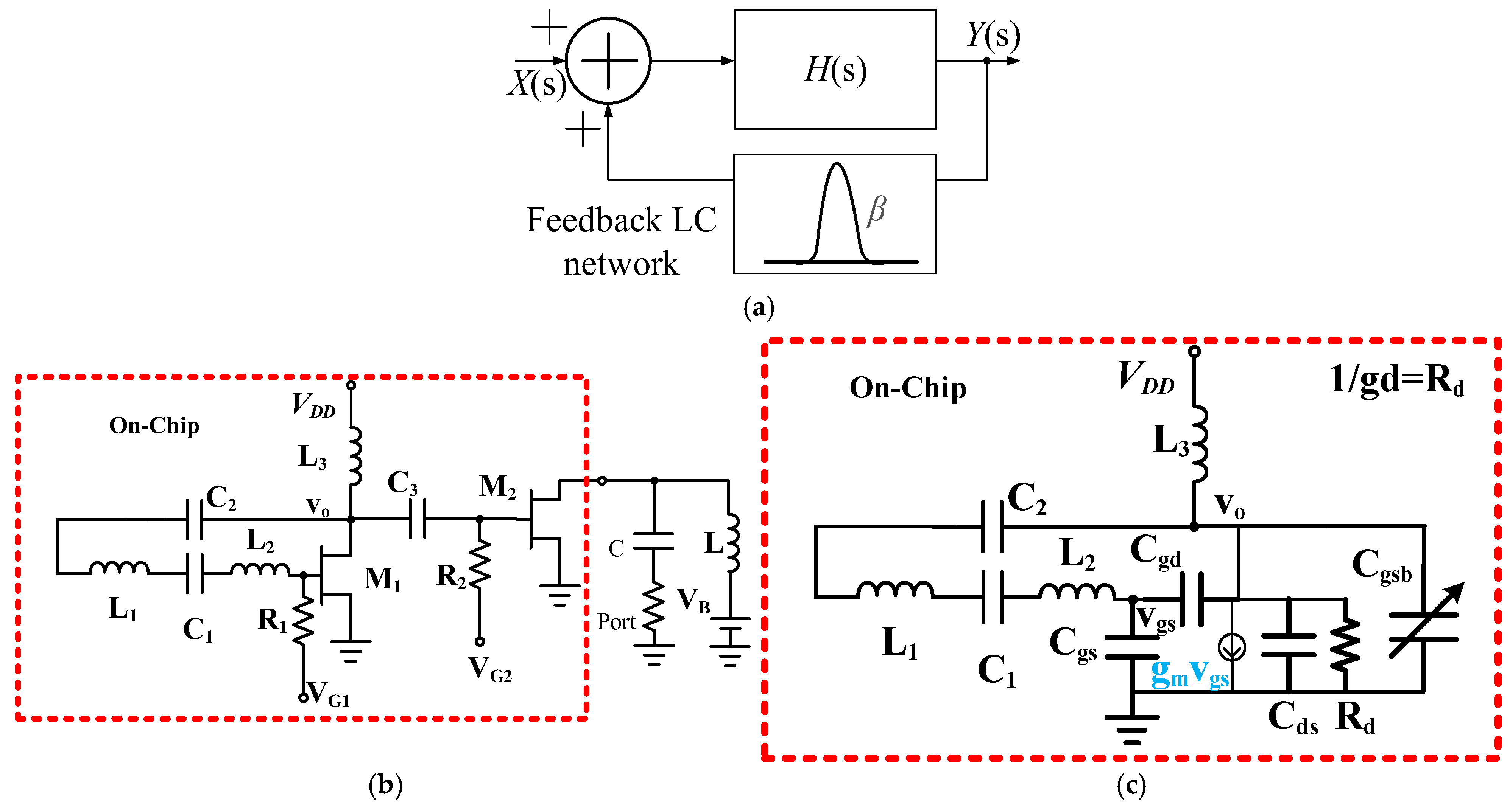
2. X-Band Feedback GaN HEMT Oscillator with Split Core and Buffer

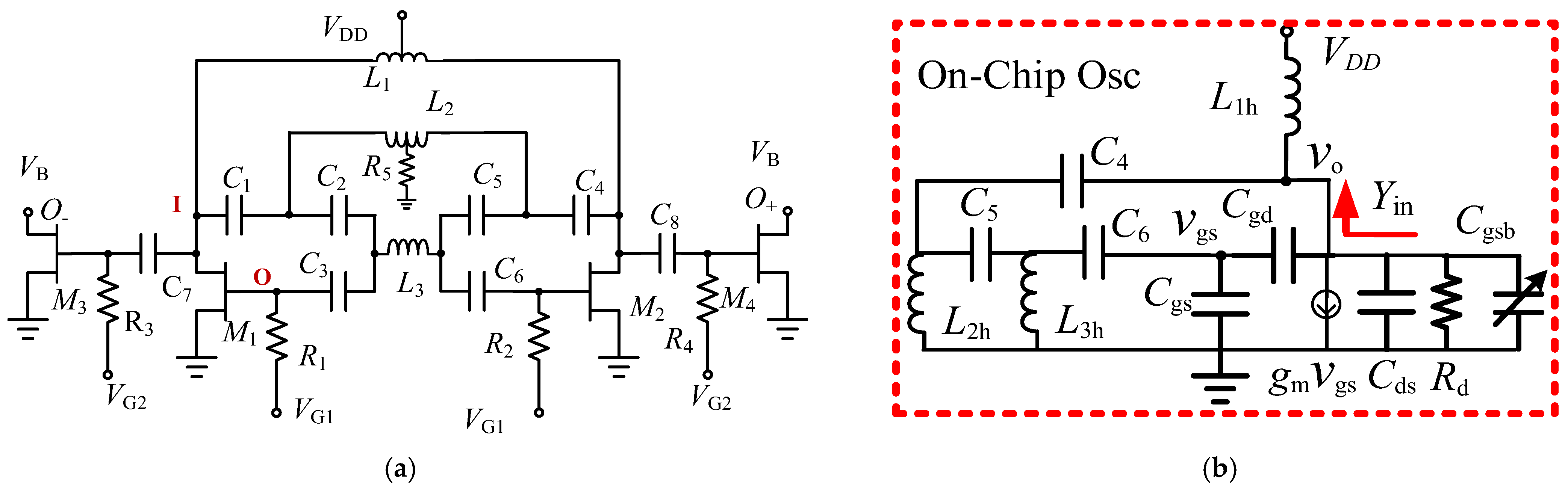
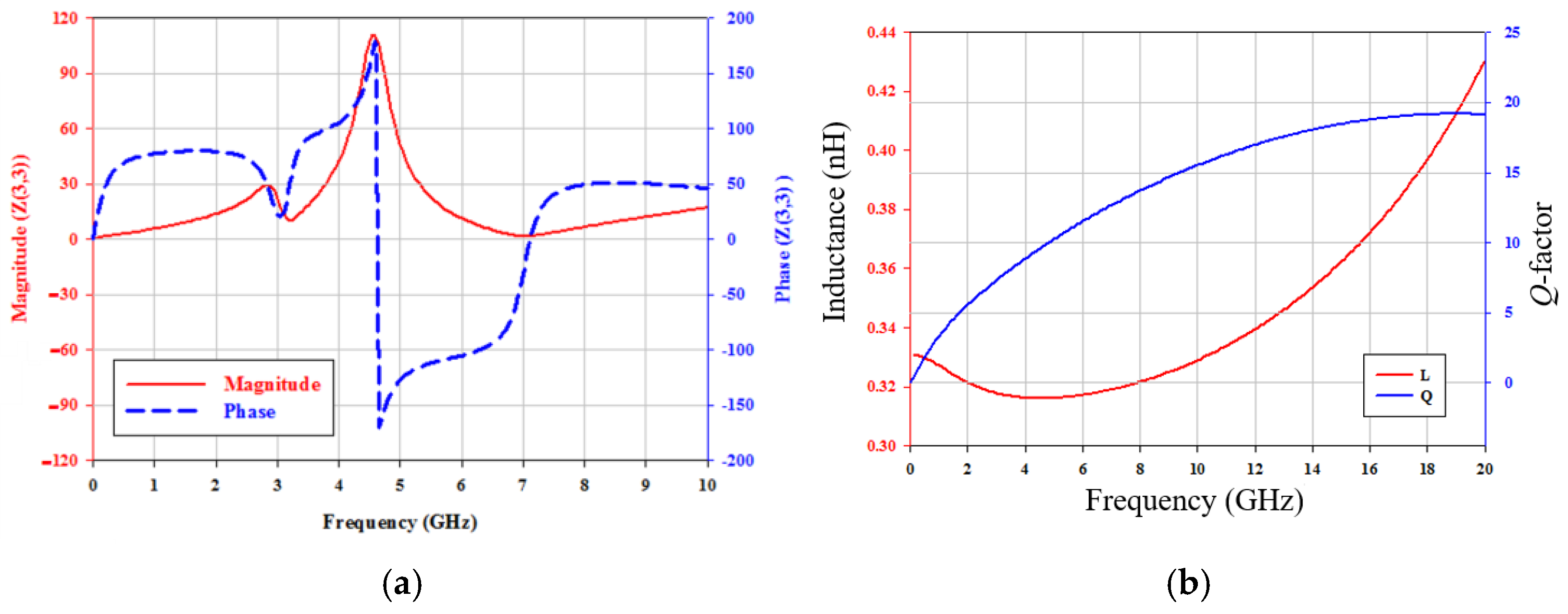
2.1. Circuit Design of the First Oscillator

Figure 1a shows a feedback oscillator generating a periodic output Y without input X = 0. The feedback network circuit β is used to select the operation frequency. The circuit can oscillate if Barkhausen’s criteria |βH(jωo)| = 1 and ∠βH(jωo) = 0° hold. Figure 1b shows the schematic of the designed single-ended GaN HEMT oscillator. It consists of an oscillator and a buffer. The inductor L3 and HEMT M1 form an amplifier, and R1 is a gate-biasing resistor, and VG1 is the gate voltage. Inductors L1 and L2, capacitors C1 and C2, and the parasitic gate-source capacitor of M1 form the feedback filter. VDD is the supply voltage and is connected to the output node of L3. The oscillator is used to drive the following buffer amplifier M2. HEMT M2 forms a buffer amplifier with gate bias at VG2 through the gate-bias resistor R2. VB is the buffer drain bias through an external bias inductor L. With different VDD and VB, the oscillator can be optimized for low phase noise performance, and the buffer is used to output high power. M1 and M2 share the same substrate stray inductance; the current of M2 affects the property of M1. Figure 1c is the simplified small-signal equivalent circuit of the designed HEMT oscillator. Cgsb is the parasitic gate-source capacitor of buffer M2. Cgs, Cds, and Cgd are, respectively, the gate-source, drain-source, and gate-drain capacitors of M1. These capacitors are bias-dependent. gm is the transconductance of M1, and gd is the output conductance due to the effect of M1 output conductance and other resistive losses. C3 is ignored for simplicity. Minimum transconductance gain is given by
g m = ω 2 L 21 C x 1 C x / C g s g d
1 C x = 1 C g s + 1 C 1 + 1 C 2 ,   L 21 = L 2 + L 1
The small-signal model for the oscillator is used to derive the resonant frequency given by
ω 2 = C x L 3 + L 3 C g s b + L 21 C x 2 L 3 C g s b L 21 C x + ( C x L 3 + L 3 C g s b + L 21 C x ) 2 4 L 3 C g s b L 21 C x 2 L 3 C g s b L 21 C x
As VDD increases, the voltage swing of Vo increases, and the average capacitance over an oscillation cycle changes. DC bias also changes the capacitance. The oscillation frequency is tunable by tuning VDD. If L3 is large, (3) simplifies to
ω = 1 L 21 C x + C g s b C g s b C x

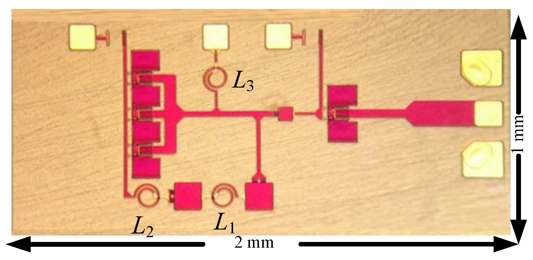
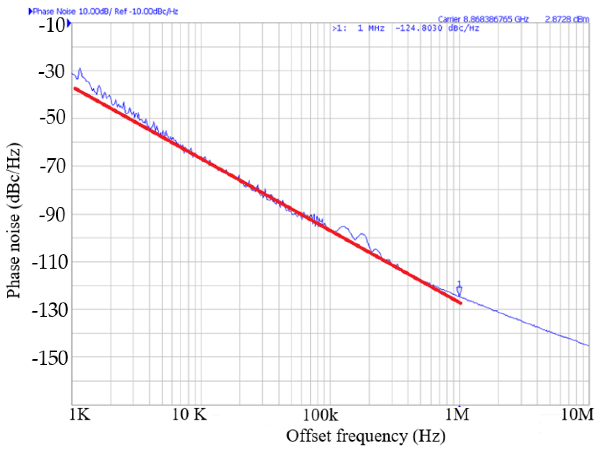
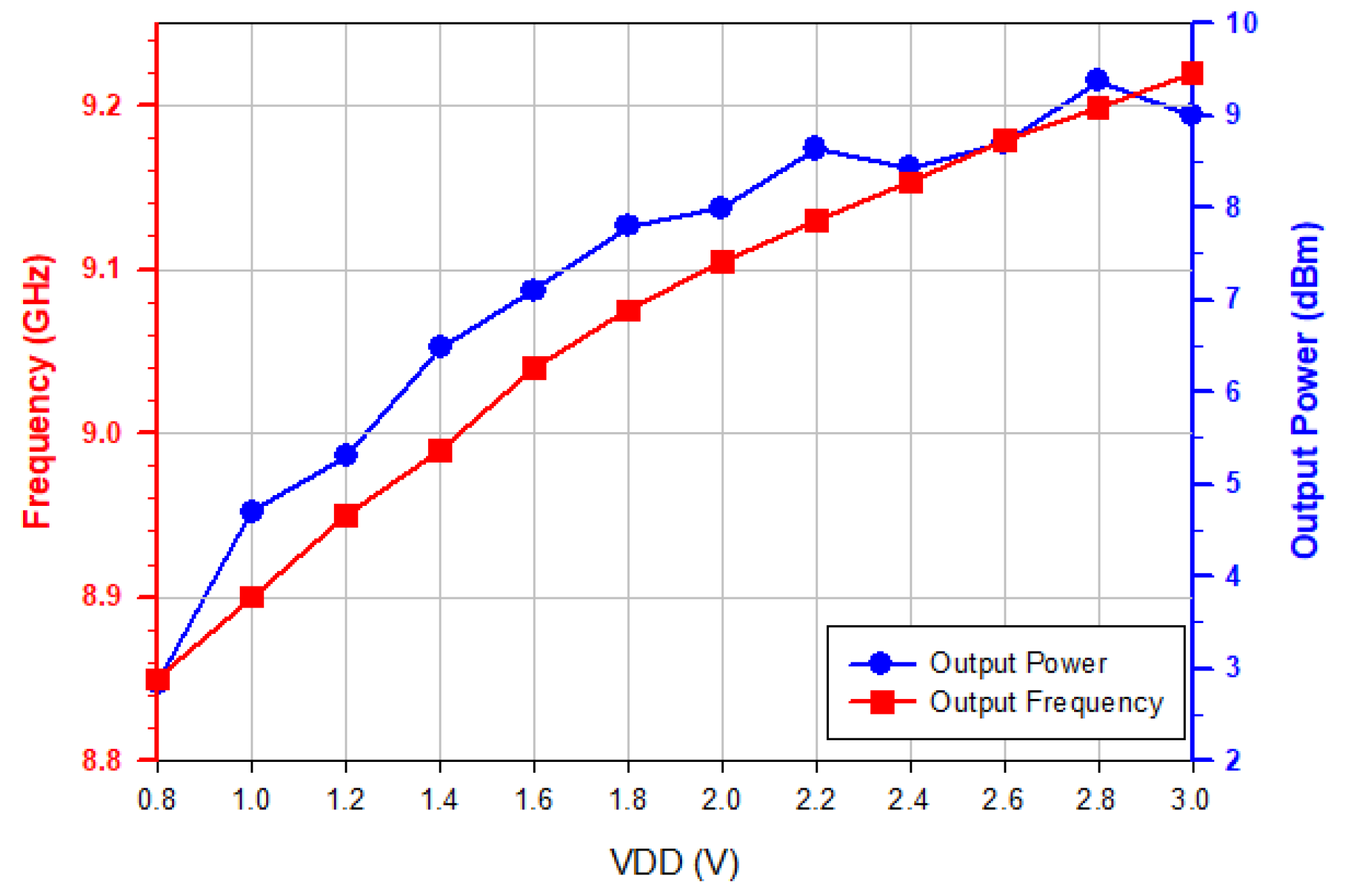
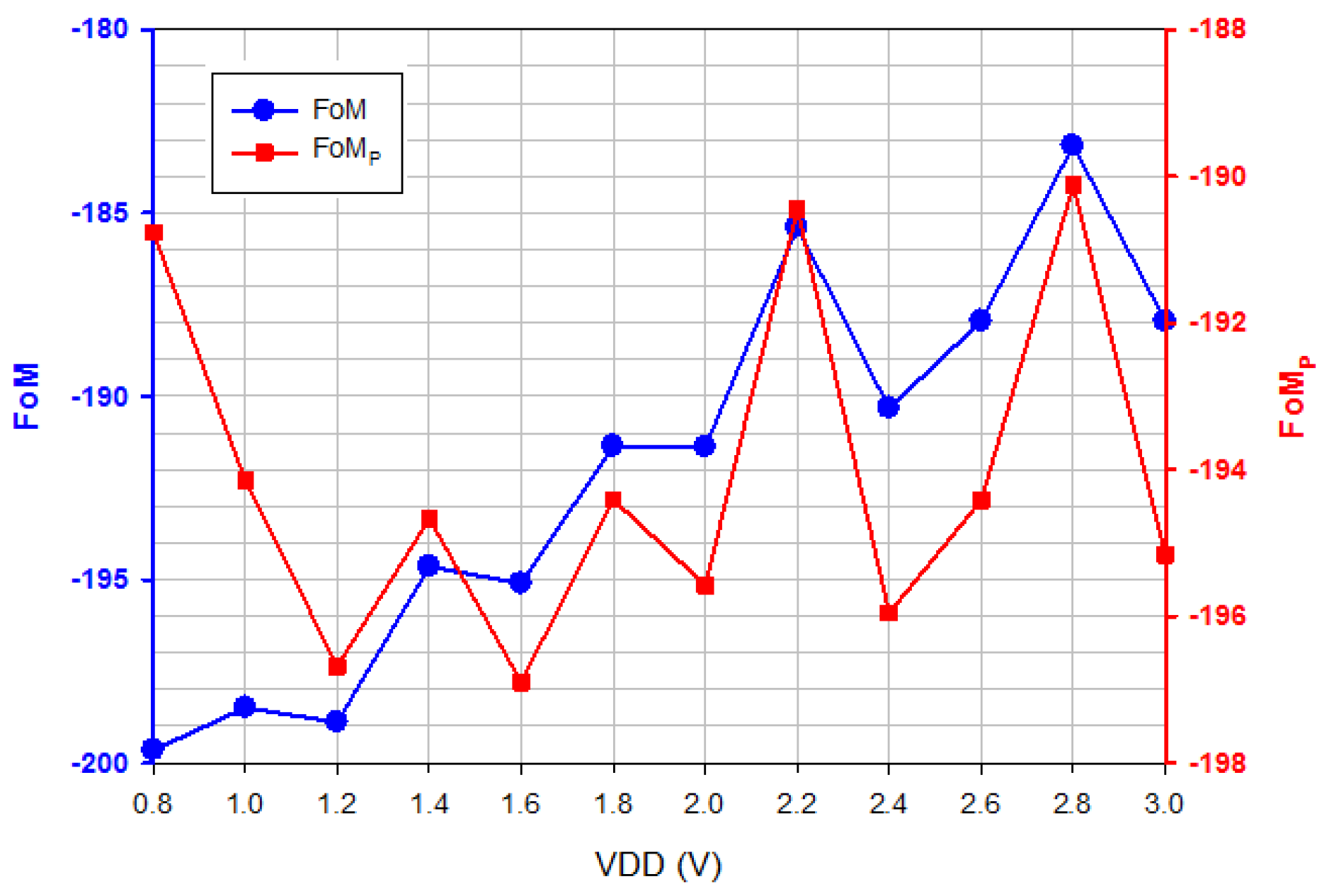
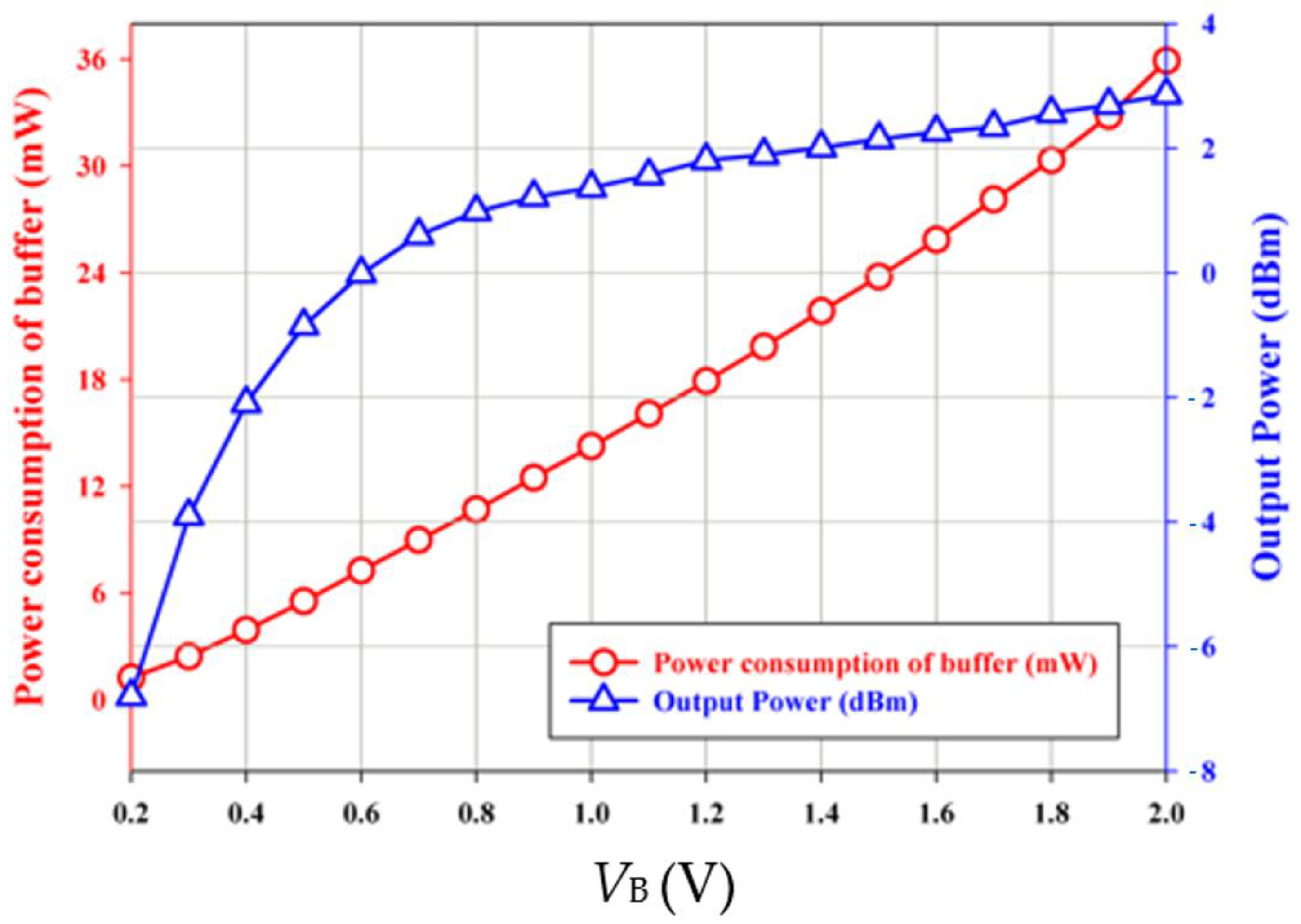
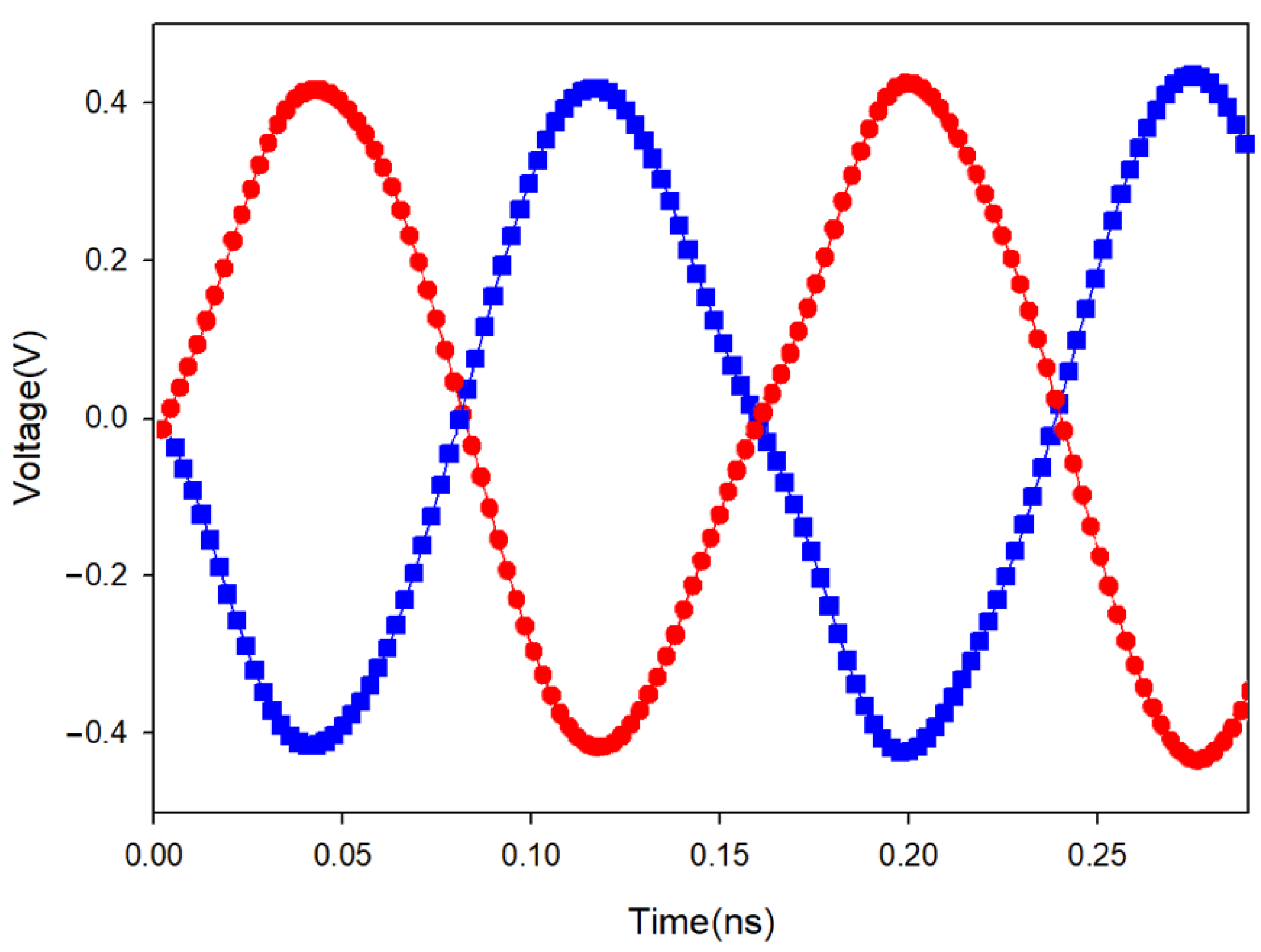
2.2. Measurement and Discussion

The first oscillators were designed and fabricated in the WIN 0.25 μm GaN/SiC HEMT process. Figure 2 shows the micrograph of the oscillator with a chip area of 2 × 1 mm2, including all test pads and dummy metal. Foundry-supplied inductors are planar circular inductors featuring a high-Q factor. Figure 3 shows the measured output characteristics of the buffer HEMT. Figure 4a shows the measured expanded output spectrum. Figure 4b shows the measured full-span output spectrum of the fundamental signal at 8.86 GHz with an output power of 3.75 dBm. At VDD = 0.8 V, the power consumption is 2.45 mW. The 2nd harmonic power is lower than the fundamental by 30.3 dB.
Figure 5 shows the measured phase noise performance of the oscillator. The phase noise of the oscillator is about −124.8 dBc/Hz at 1 MHz offset frequency from 8.86 GHz oscillation frequency and has a slope of −30 dB/dec in the low frequency offset. The phase noise is mainly due to the upconversion of device flicker current noise. Figure 6 shows the measured oscillator frequency and output power. As VDD increases, the output power increases, the capacitance decreases, and the oscillation frequency fosc increases.
The figure of merit (FoM) defined in Equation (5) is used to benchmark the performance of oscillators:
FOM = L ( ω o , Δ ω ) + 10 log P D C 20 log ω o Δ ω
where ωo is the fundamental frequency, ∆ω is the offset frequency, L {∆ω} is the phase noise at ∆ω, and PDC is the DC power consumption of the oscillator in mW. By the calculation, the FoM of the first oscillator is −199.8 dBc/Hz.
Figure 7 shows the effect of buffer bias VB on oscillator performance. As VB increases, output power from the buffer increases, and power dissipation in the oscillator core decreases. Oscillation frequency is insensitive to VB, and minimum phase noise is measured at VB = 1.4 V. Considering the effect of buffer power consumption, a new FOM is defined by
FOM p = L ( Δ ω ) + 10 log P c o r e + P b u f f e r P o u t 20 log ω o Δ ω
POUT is the output power of the buffer, and PBuffer is the buffer power consumption. Figure 8 shows a comparison of FOM and FOMp versus VDD. FOM decreases with VDD, and FOMP is relatively insensitive to VDD because PCore is smaller than PBuffer. The phase noise of the oscillator is due to the AM-PM up-conversion caused by the device’s current noise and voltage-dependent capacitance. Table 1 shows the performance comparison. A GaN HEMT has deep-level defects located on the surface, barrier, or buffer layer of the device; the presence of deep-level defects could contribute to low-frequency current noise. It was found that the low-frequency current noise of GaN HEMT [11,12] is dominated by the flicker noise. The low-frequency current noise of M1 flows into Cgs, Cds, and Cgd, changes the capacitor voltage, and causes the fluctuation of average capacitance and oscillation frequency [13].

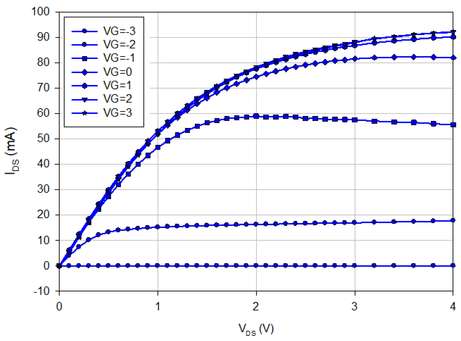
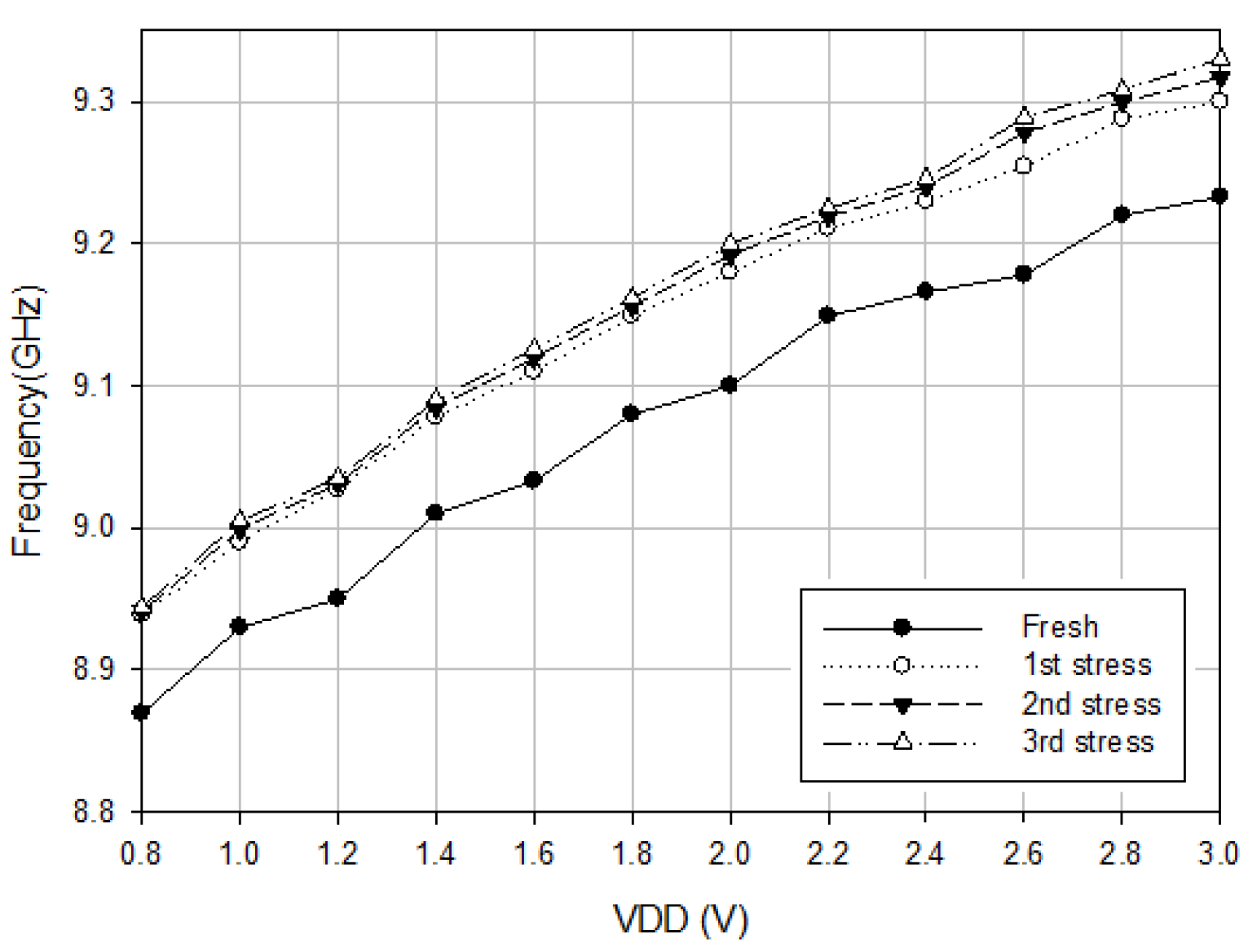
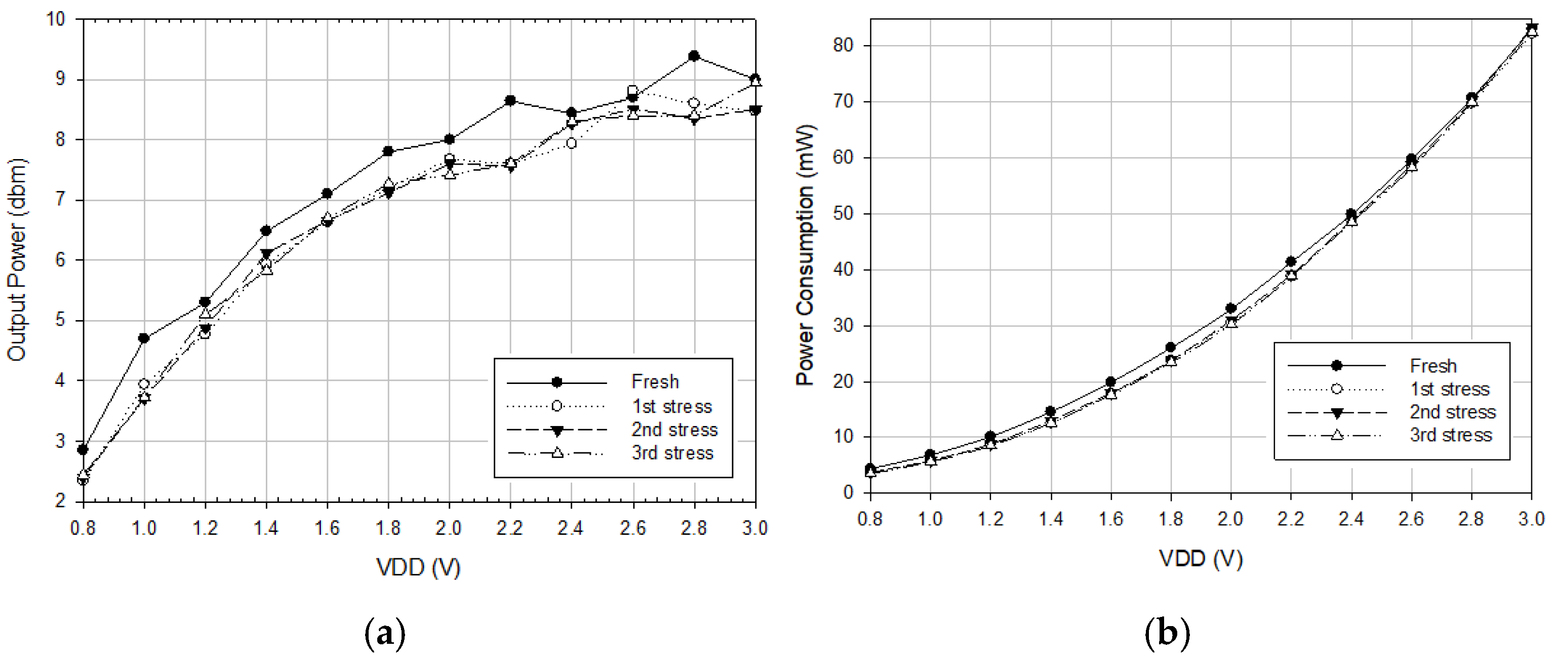
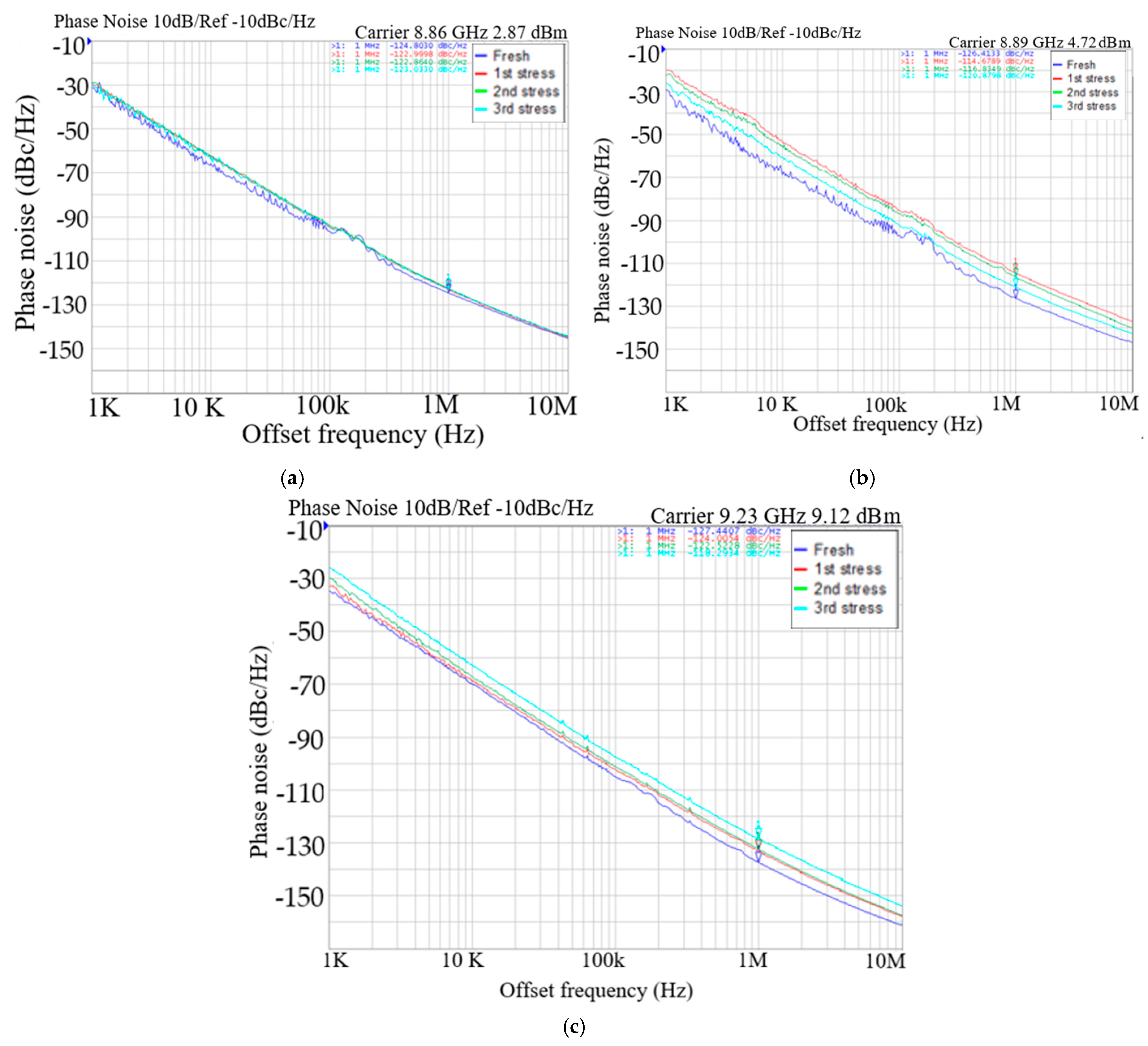
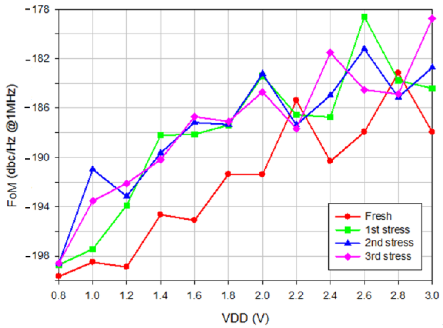
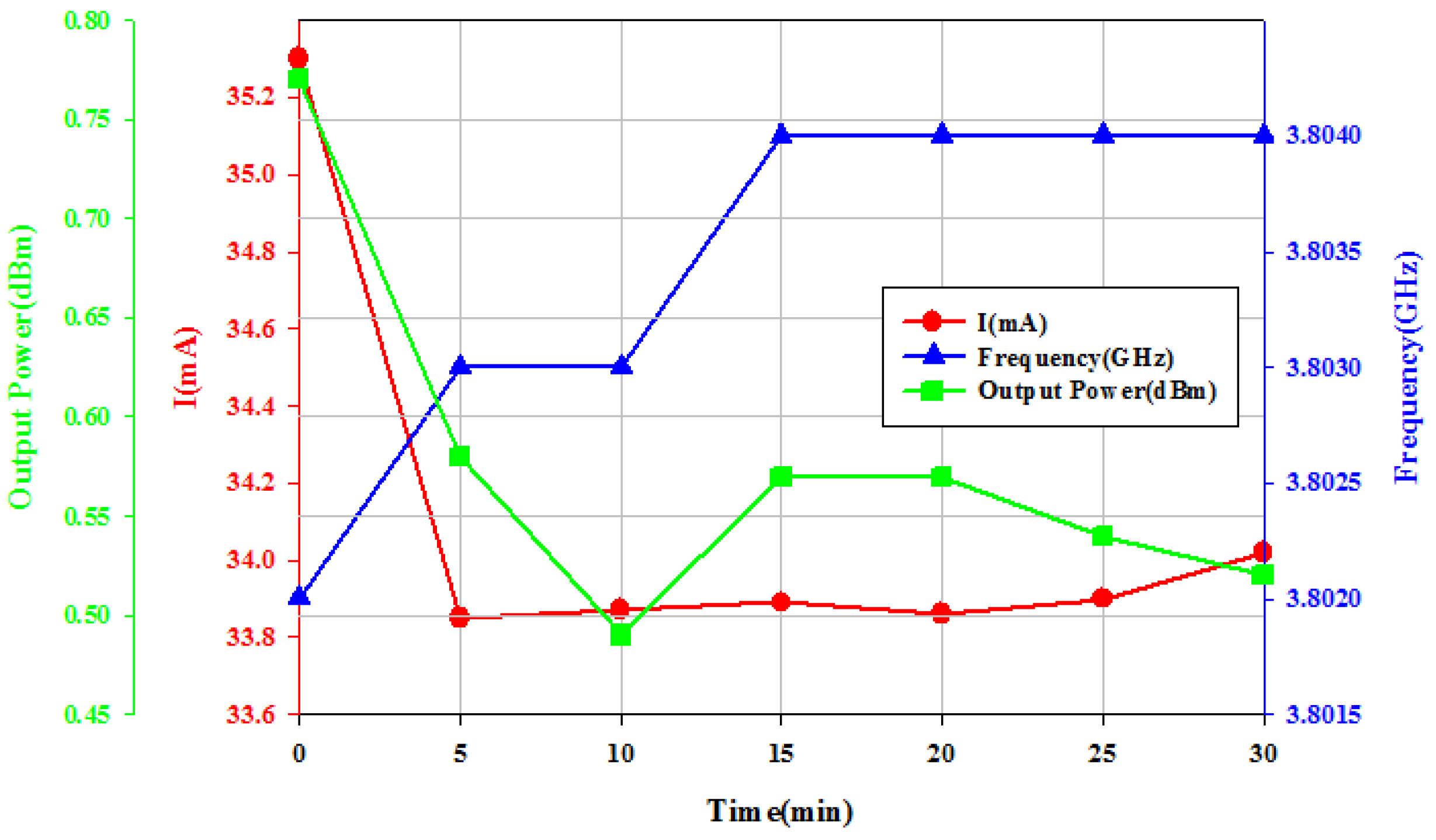
2.3. Drift of GaN HEMT Oscillator Performance with High Operating Bias

High-power GaN HEMT oscillators operate the HEMTs in the high field with the hot-carrier stress causing the electron trapping and the creation of interface states, which increase the phase noise of the oscillator. In this subsection, the degradation of the oscillator with HEMTs subjected to hot-carrier injection is discussed. The stressed oscillator is subject to higher drain voltage operation: VDD = 8 V, VG1 = −2.4 V, VG2 = 0 V, VB = 0 V for 90 min, which is divided into three time steps classified at t = 0, 30, 60, and 90 min for measuring the time-dependent oscillator performance at low supply voltage while the buffer is on. Figure 9 shows the measured oscillation frequency versus VDD, and the oscillation frequency increases with VDD. The stress increases the oscillation frequency. The oscillation frequency is related to the tank capacitance; the stress increases the oscillation frequency, and a high supply voltage bias reduces the capacitance.
Figure 10a shows the measured oscillator output power versus VDD, where the VDD increases the output power. Figure 10b shows measured power consumption versus VDD. The stress reduces the oscillator’s output power and power consumption. Figure 11a, Figure 11b, and Figure 11c show, respectively, the measured phase noise versus stress step at VDD = 0.8, 1, and 3 V, indicating that the fresh phase noise is the smallest at low and high offset frequencies. Figure 12 shows measured phase noise at 1 MHz offset frequency versus VDD. At VDD = 0.8 V, VG1 = −2.4 V, VB = 3 V, VG2 = −2 V, the measured fresh phase noise of the oscillator is about −124.8 dBc/Hz at 1 MHz offset frequency from the carrier frequency 8.86 GHz. Figure 13 shows the FOM versus VDD. The high drain bias increases phase noise and degrades the FOM at VDD < 2 V.
For the next stress experiment, the buffer is subjected to higher drain voltage operation: VG1 = 0 V, VDD = 0 V, VG2 = −2.2 V, and VB = 8 V for 30 min, and the VCO-core is under low supply voltage. Figure 14a shows the measured output characteristics of buffer HEMT before and after the high buffer bias. Figure 14b shows measured oscillation frequency versus VB, and Figure 14c shows measured phase noises versus step stress. The buffer stress alone does not change the oscillation frequency and phase noise of the oscillator under low supply bias. This indicates that biasing the oscillator core at low supply and the buffer at high supply voltage is a good operation condition for large output power because high FOM is maintained. To gain high output power, the buffer supply voltage is increased.

3. Balanced GaN HEMT Oscillator with Left-Handed Transmission Line Filter

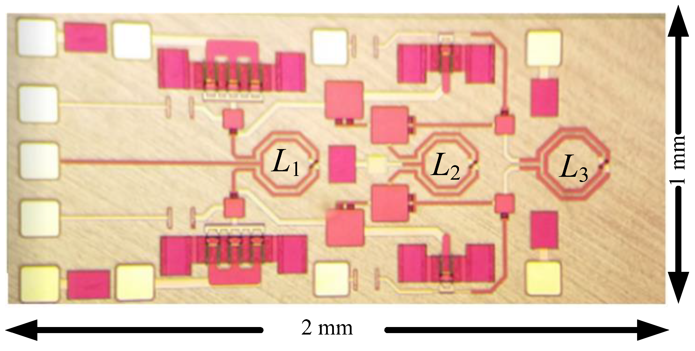
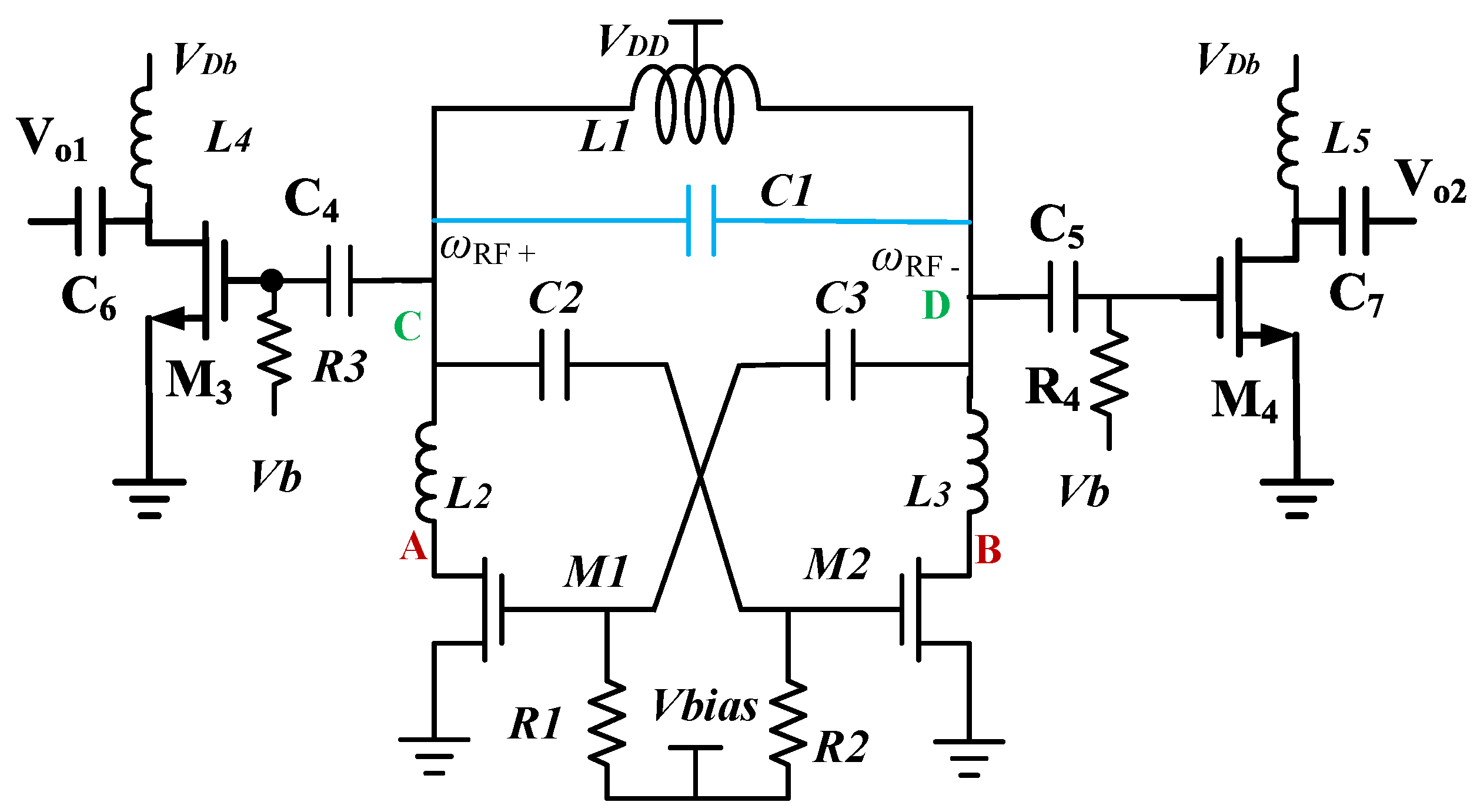
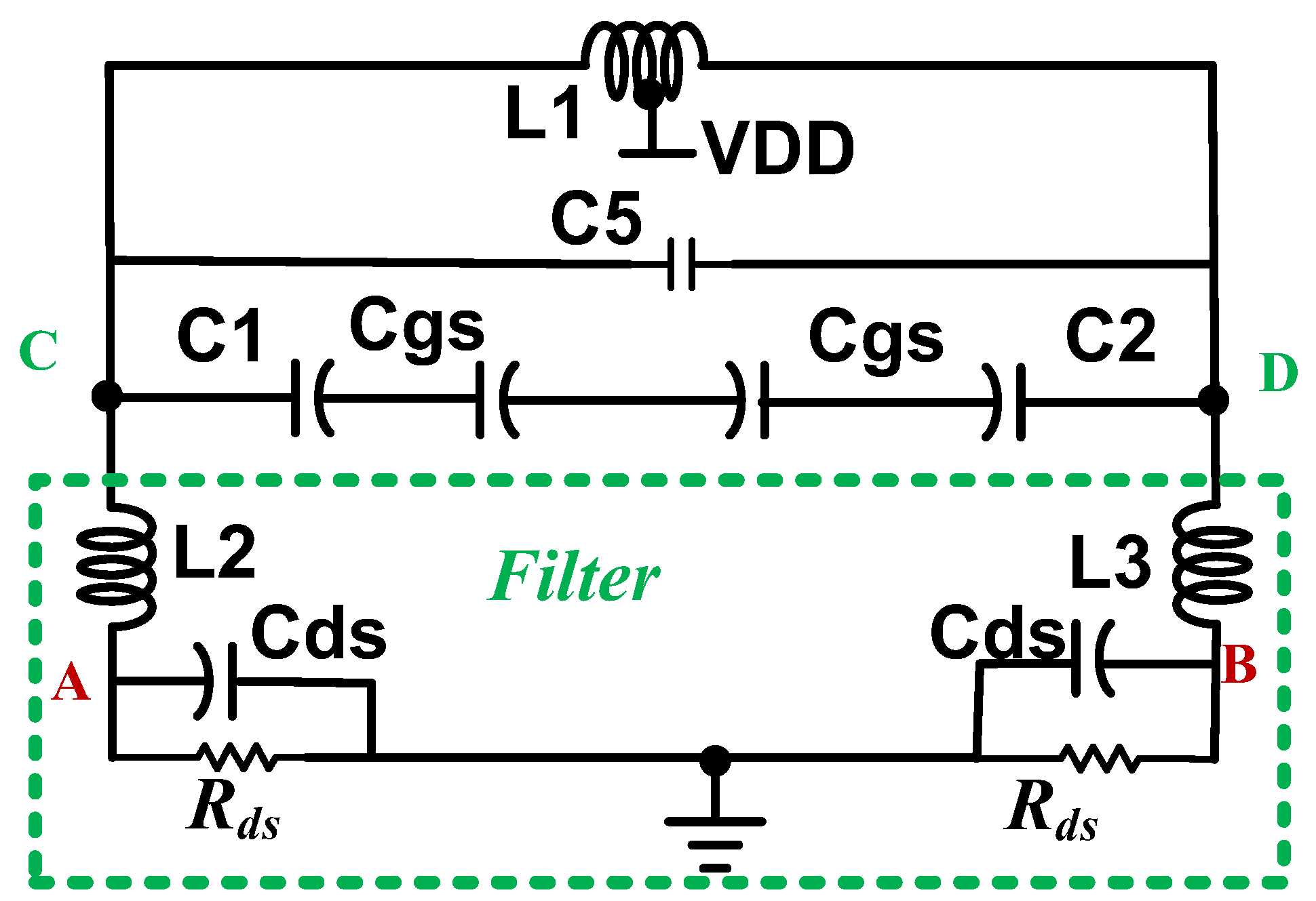
3.1. Circuit Design of the Balanced Oscillator

The previous oscillator is a single-ended circuit, and this section discusses a balanced oscillator using two identical single-ended oscillators configured in a balanced structure. In the balanced oscillator, the feedback network can be a lossless transmission line (TL) such as a right-handed TL (RH-TL) consisting of a series inductor L1 and parallel capacitor C, as shown in Figure 15a, or a left-handed TL (LH-TL) consisting of a shunt inductor L1 and series capacitor C, as shown in Figure 15b; the composite right/left-handed TL (CRLH-TL) is a general TL with a combination of the RH-TL and LH-TL. The LH-TL [14] and CRLH-TL [15,16] have been used to design CMOS cross-coupled oscillators. The present GaN HEMT balanced oscillator employs the LH-TL as the feedback network by cascading three LH-TL unit cells.
Figure 16a shows the schematic of the designed fixed-frequency GaN HEMT oscillator. It consists of two single-ended sub-oscillators sharing the same virtual ground. The first sub-oscillator consists of a feedback filter and an amplifier formed with inductor L1 and HEMT M1. R1 is a gate-biasing resistor, and VG1 is the gate voltage for M1. Inductors L1, L2, and L3, capacitors C1, C2, and C3 form a left-handed filter for feedback from the output at the I-node to the input of the amplifier at the O-node. The circuit of a standing wave oscillator (SWO) uses an open-ended TL. The filter acts as an impedance transformer between the input and output of the amplifier, and it also provides a phase response to set the oscillation frequency. VDD is the supply voltage. The second sub-oscillator consists of the same components as the first sub-oscillator. The common node of L2 and R5 is a virtual ground for the differential mode signals, and the common mode signal will develop a voltage at this node. R5 is the resistor used to diminish the common-mode oscillation. HEMT M3 and M4 forms buffer amplifiers with gate bias at VG2 through the gate-bias resistors R3 and R4. VB is the buffer drain bias through an external bias inductor L. The I-port shows the largest voltage swing, and the O-port shows the smallest voltage swing; both ports show opposite voltage phases. C1 and L2 cause a phase shift and decrease the voltage swing.
In Figure 16b, a single-ended equivalent small-signal circuit for the designed oscillator is shown. Cgs, Cds, and Cgd are, respectively, the gate-source, drain-source, and gate-drain capacitors of M2. Cgsb is the capacitor owing to C8 in series with the gate-source capacitor of M4. These parasitic capacitors are bias-dependent. Device flicker noise and thermal noise are up-converted to oscillator phase noise through these capacitors via the AM-PM modulation. gm is the transconductance of M2, and gd is the output conductance due to the effect of M2 output conductance and other resistive losses. The input impedance Yin shows the effect of a high-pass 6th–order resonator. If Cgd is ignored, then Yin is given by
Y i n = d e n sL 1 h n u m
n u m = s C 4 x sL 2 h { 1 + s 2 L 3 h [ C 6 x + C 5 x ] } + 1 + s 2 [ L 3 h C 6 x + L 3 h C 5 x + L 2 h C 5 x ] + s 4 L 2 h C 5 x L 3 h C 6 x ]
d e n = 1 + s 6 L 1 h C 4 x L 2 h C 5 x L 3 h C 6 x + s 2 [ L 3 h C 6 x + L 3 h C 5 x + L 2 h C 5 x + C 4 x L 2 h + L 1 h C 4 x ] + s 4 { L 2 h C 5 x L 3 h C 6 x + C 4 x L 2 h L 3 h [ C 6 x + C 5 x ] + L 1 h C 4 x [ L 3 h C 6 x + L 3 h C 5 x + L 2 h C 5 x ] }
If C5 and L2h are removed, the input admittance of the 4th-order resonator becomes
Y i n = 1 + s 2 [ L 3 h C 6 x + L 3 h C 4 x + L 1 h C 4 x ] + s 4 L 1 h C 4 x L 3 h C 6 x sL 1 h { 1 + s 2 L 3 h [ C 6 x + C 4 x ] }
The resonant frequency is obtained by setting Yin = 0.
ω 2 = L 3 h C 6 x + L 3 h C 4 x + L 1 h C 4 x 2 L 1 h C 4 x L 3 h C 6 x ± [ L 3 h C 6 x + L 3 h C 4 x + L 1 h C 4 x ] 2 4 L 1 h C 4 x L 3 h C 6 x 2 L 1 h C 4 x L 3 h C 6 x
The oscillation frequency should obey the Barkhausen criteria. Figure 17a shows the simulated input impedance at the drain of M1, with a peak resonant frequency of 4.56 GHz. The second resonant frequency is 2.9 GHz, and the third resonant frequency is out of the x-axis plot. Figure 17b shows the simulated inductance and Q-factor of the inductor L1. The inductance is 0.316 nH, and the Q-factor is 9.643 at 4.56 GHz.

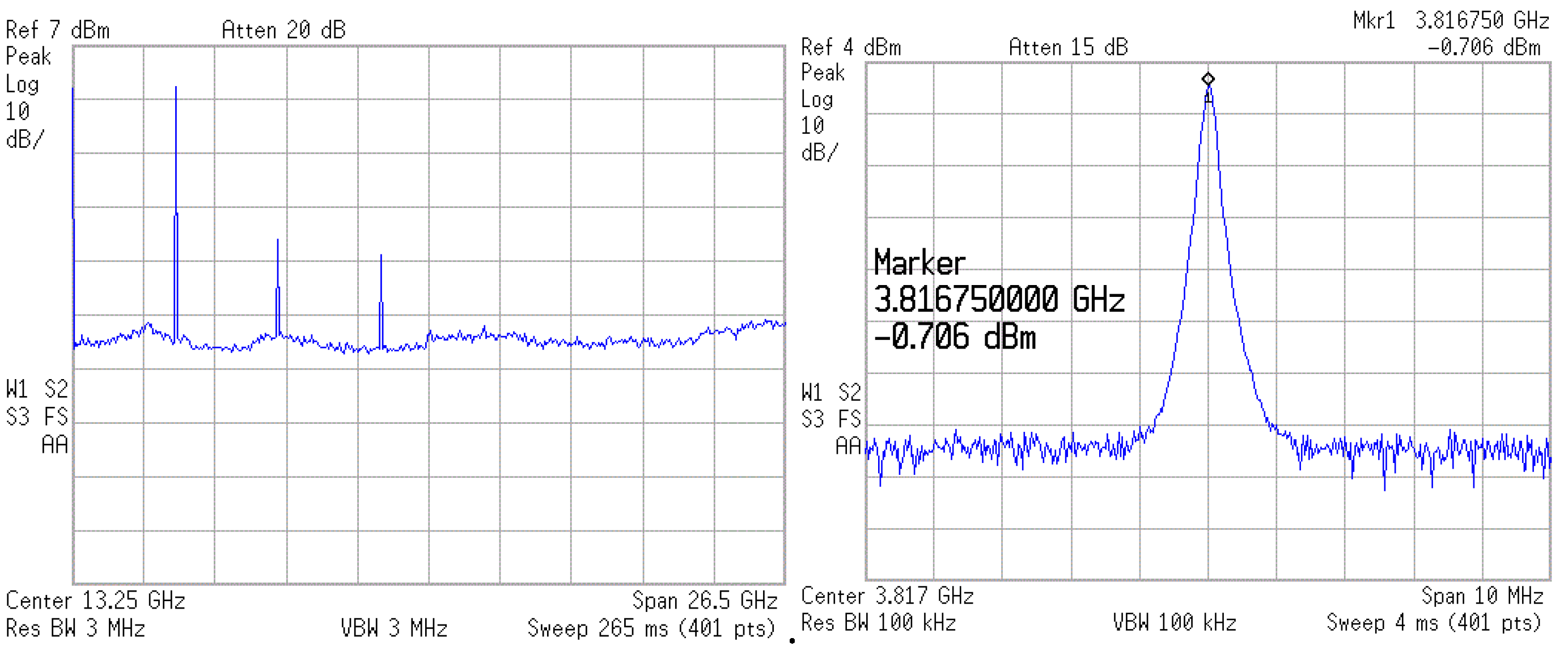
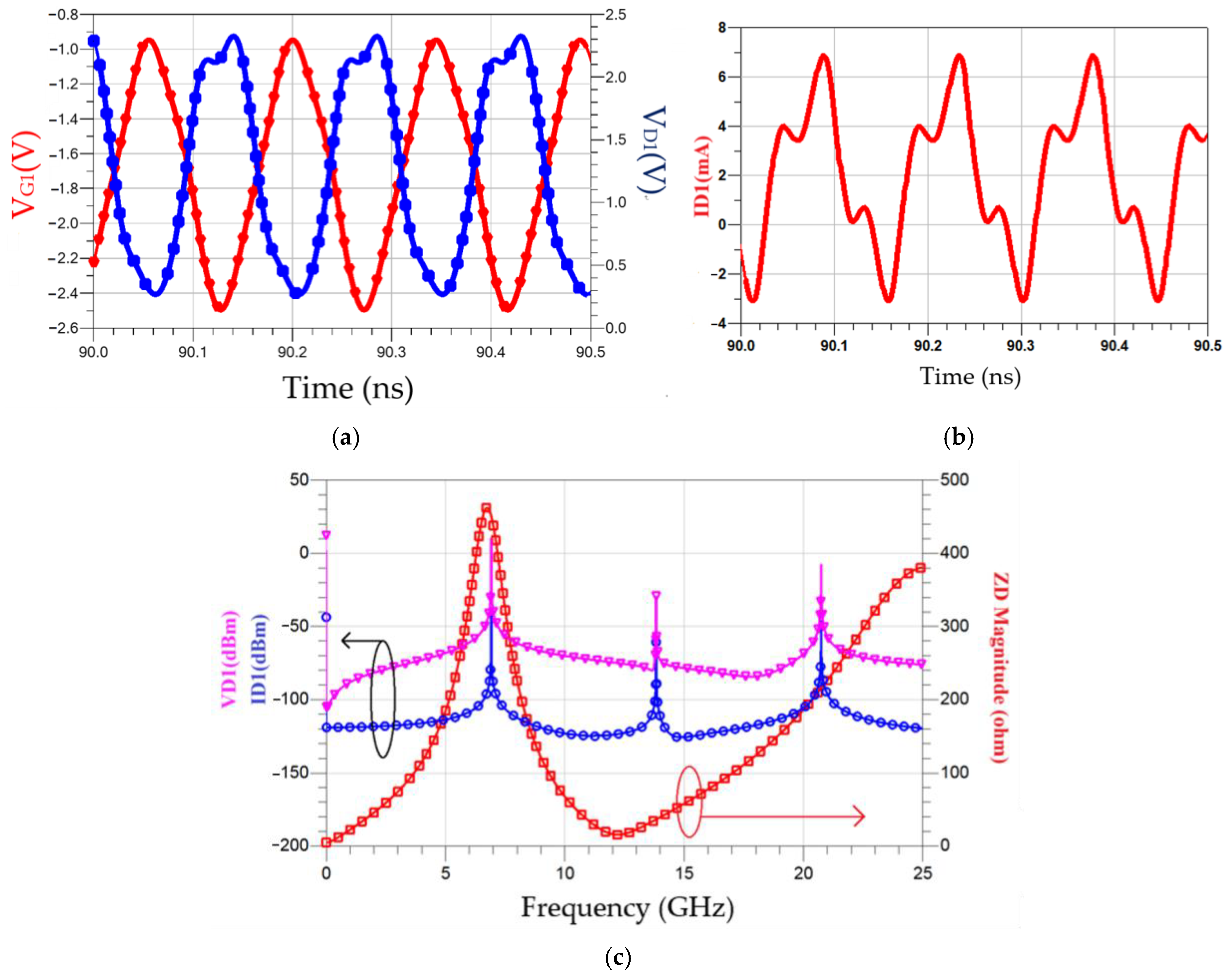
3.2. Measurement and Discussion

The oscillators were designed and fabricated in the WIN 0.25 μm GaN/SiC HEMT process. Figure 18 shows the micrograph of the second oscillator with a chip area of 2 × 1 mm2, including all test pads and dummy metal. Two center-tapped and one symmetric inductor are used. The die was attached to the PCB using epoxy for characterization. Figure 19 shows measured output voltages; differential signals are measured for the balanced oscillator. Figure 20 shows the measured output spectrum of the fundamental signal at 3.81 GHz with an output power of −0.706 dBm.
To investigate the effect of varying supply bias on the phase noise of the balanced oscillator, the gate bias is fixed at −2.2 V and the supply bias is changed from 0.6 V to 2 V. Figure 21 shows the phase noise performance of VCO biased at VDD = 0.6 V~2 V. At VDD = 1.6 V, the power consumption is 31.36 mW, the measured phase noise of oscillator is about −131.73 dBc/Hz at 1 MHz offset frequency from 3.818 GHz oscillation frequency and has a slope of −20 dB/dec in the high frequency offset. The corner frequency increases as VDD increases. By the calculation, the FOM is −188.4 dBc/Hz. Figure 22 shows measured frequency, phase noise at 1 MHz offset, output power, and current consumption versus VDD. As versus VDD increases, the phase noise decreases, the oscillation frequency slightly increases, and the output power increases. Figure 23 shows the measured power consumption and output power of the buffer versus VB. Power consumption and output power of the buffer increase with increasing VB because of enhanced channel conductance. The thermal noise-related phase noise is more sensitive to the supply variation than the flicker noise-related phase noise. Increasing the supply voltage is an effective way to reduce phase noise at high offset frequencies at the cost of power. The phase noise associated with thermal noise reduces as VDD increases, while the phase noise at low offset frequency is not sensitive to supply bias; the latter is owing to device flicker noise. Table 1 is the performance comparison.

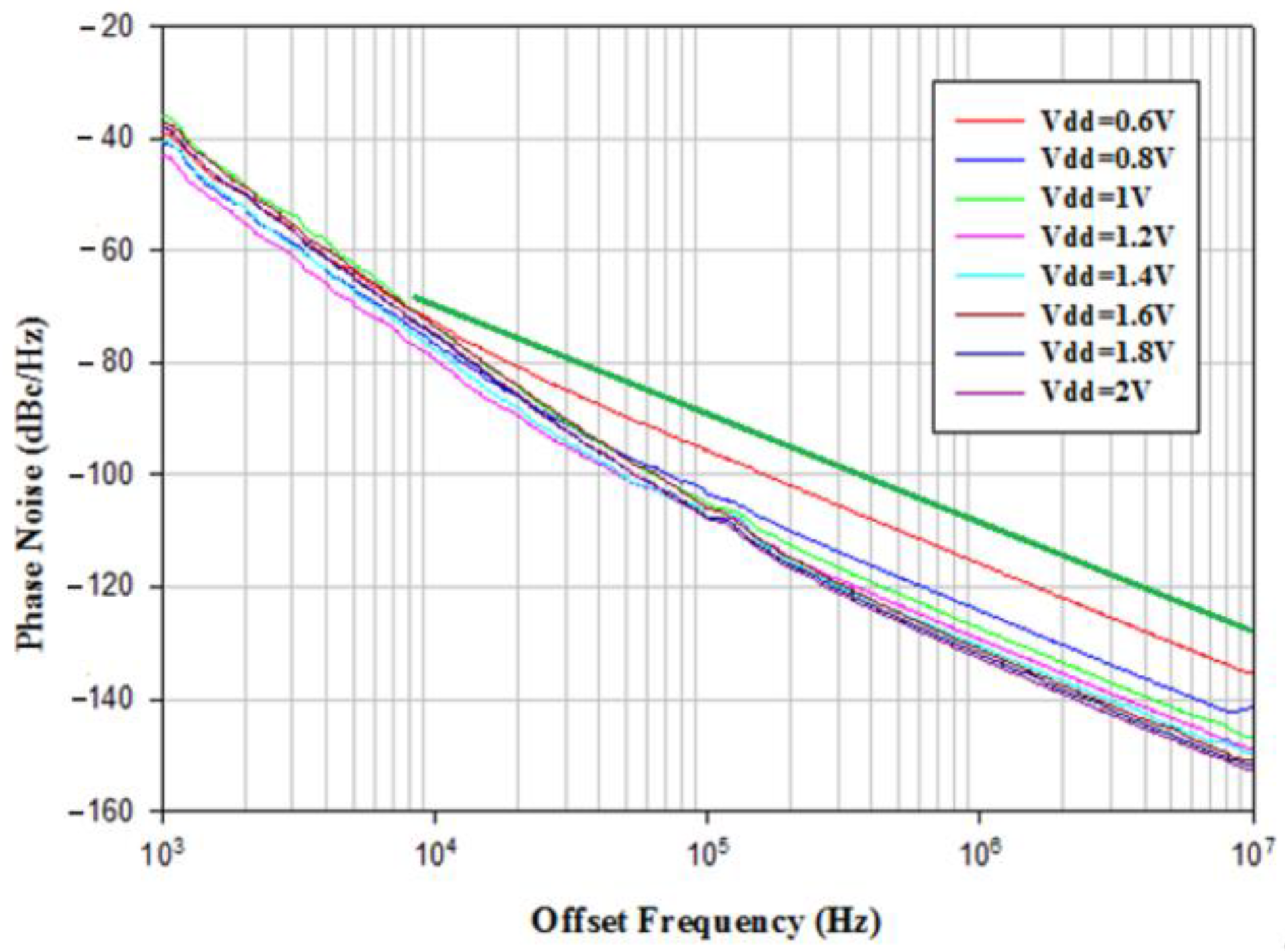
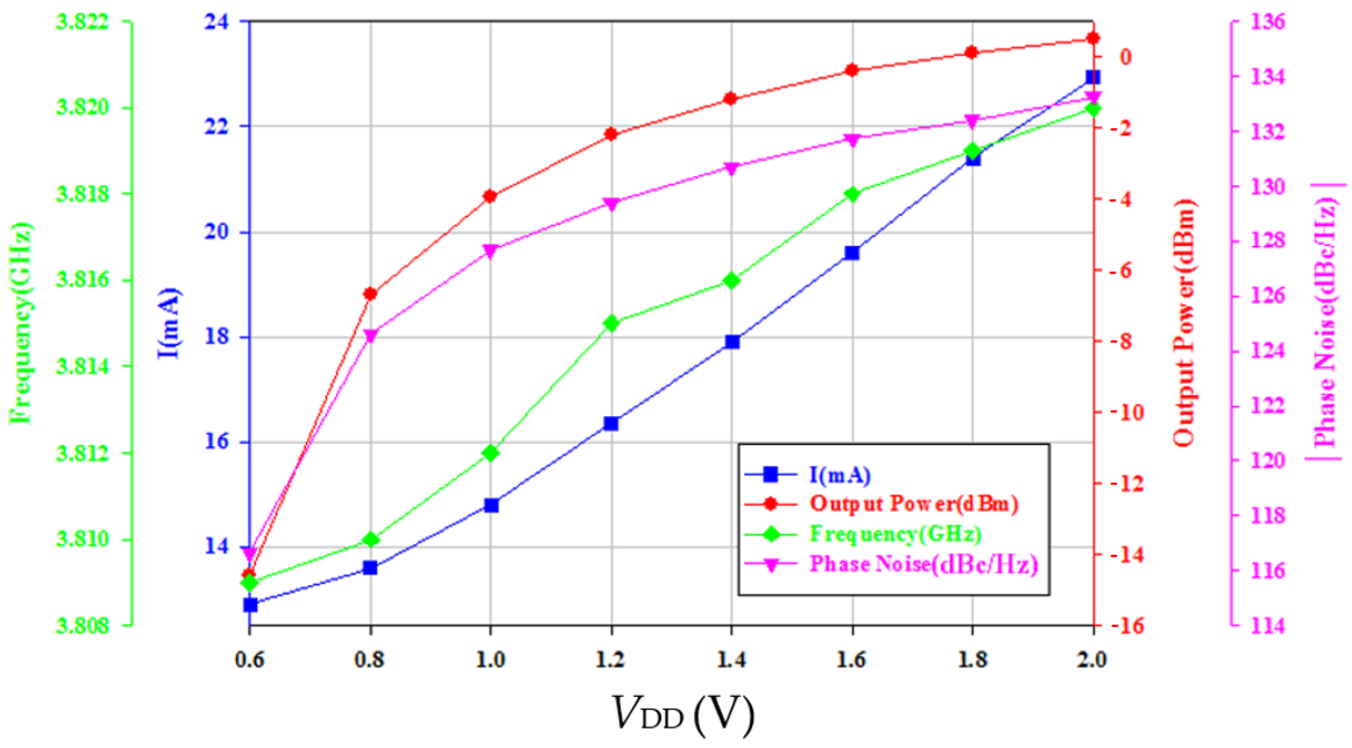
3.3. High-Supply Voltage Effect

The 2nd experiment was carried out by biasing the buffer at low supply and biasing the oscillator-core at VDD = 15 V for 30 min; the output power and consumption decrease versus bias time, tbias, as shown in Figure 24. Measured data shows the effect of the VCO-core subject to the high VDD bias. The hot-carrier stress causes degradation in oscillator parameters. Figure 25a shows measured phase noise after the stress time for tbias= 0, 30, and 60 min. At 1 MHz offset frequency, the phase noise increases with bias time. Figure 25b shows measured phase noise at a 1 MHz offset frequency; the degradation occurs at low supply voltage.

4. GaN HEMT Oscillator with Implicit-Resonator
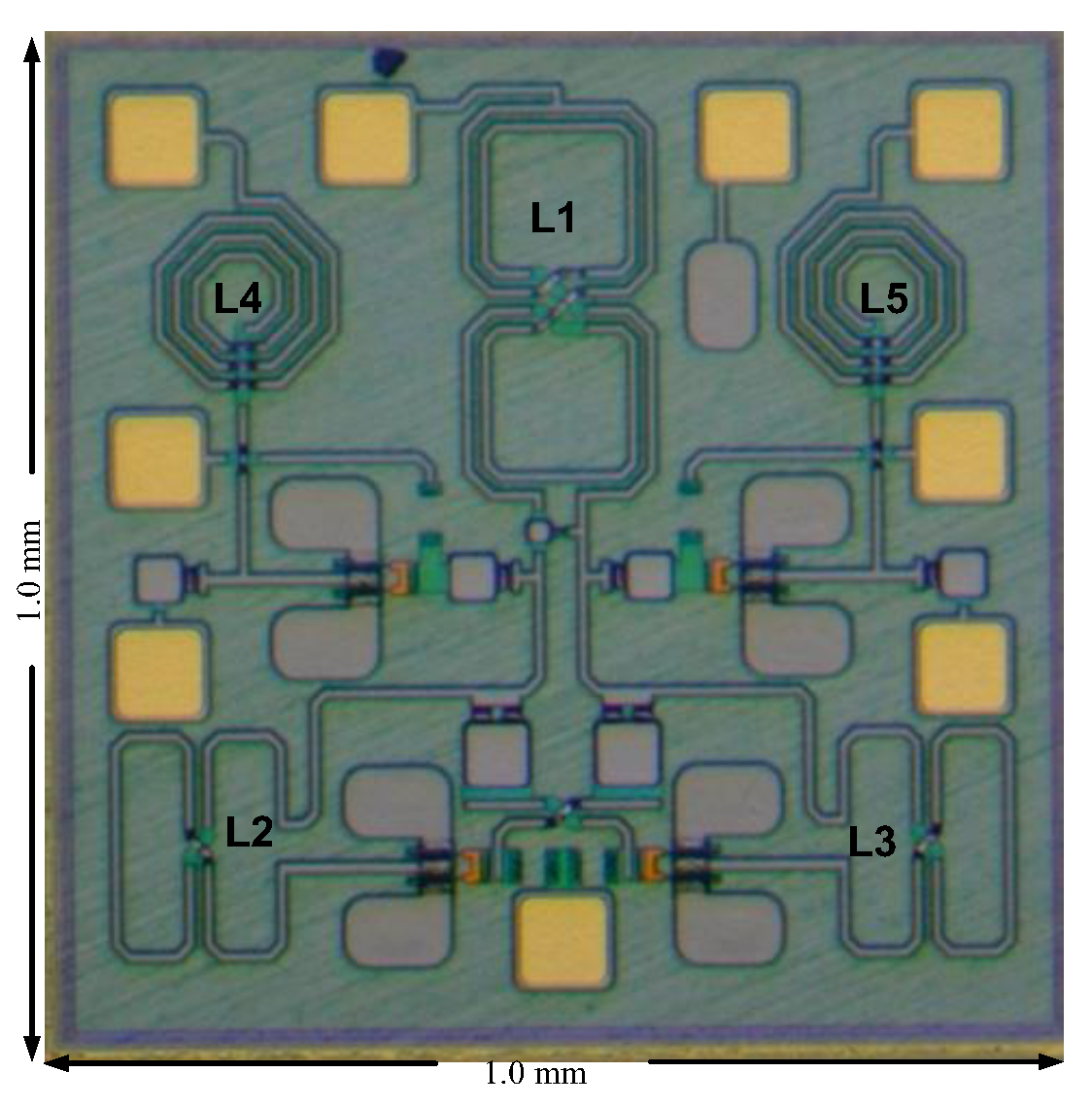
Depending on the RF applications, the GaN oscillator can be classified as either a voltage-controlled oscillator (VCO) or a fixed-frequency oscillator (FFO) [20]. This section designs a third GaN HEMT cross-coupled FFO using a two-turn 8-shaped inductor to reduce the magnetic coupling noise and a degenerated-drain inductor to reduce the phase noise. The 8-shaped inductors are configured with 1-turn [21], 2-turn [22], 3-turn, and 4-turn structures and have not been used in GaN circuits.

4.1. Circuit Design

Figure 26 shows the FFO schematic. The FFO is designed using the WIN 0.12 μm RF GaN on SiC technology. Two 1-turn 8-shaped inductors (L2, L3) could improve the tank Q-factor, while (M1, M2) show channel resistance operating in the linear regime. Two-turn eight-shaped L1, capacitor C1, and parasitic capacitors (Cv1, Cv2) of HEMTs (M1, M2) resonate at the fundamental carrier. VDD is the supply, and VBias is the gate bias. The three-and-a-half-turn spiral inductors (L4, L5) are buffer loads using a bias circuit (C4, R3). The pair (M1, M2) provides the negative differential resistance, compensating for the loss of the LC tank.
Figure 27 shows the equivalent circuit of Figure 26 with the dual resonant network by replacing M1 with the drain-source capacitor Cds and channel resistor Rds. L2 in series with Cds forms the harmonic resonator. Neglecting Rds, C1, and Cgs for simplicity, the two resonant frequencies are
ω 2 = C 5 L 1 + L 2 C d s + 0.5 L 1 C d s 2 C 5 L 1 L 2 C d s ± [ C 5 L 1 + L 2 C d s + 0.5 L 1 C d s ] 2 4 C 5 L 1 L 2 C d s 2 C 5 L 1 L 2 C d s
From the nodes A and B, C5 and (L2, L3) form the filter effect. Cds, Cds, and (L2, L3) form the harmonic resonance. The impedance peak seen between the nodes A and B is larger than the impedance peak seen between the nodes C and D. This is caused by (L2, L3).
Figure 28a shows the simulated phase noise. Inductors (L2, L3) reduce the phase noise. The simulated phase noise is −119.3 dBc/Hz (−121.5 dBc/Hz) without (with) drain inductor. Figure 28b shows the three simulated tank impedances. The differential-mode (DM) impedance in purple color is from a reference VCO shown in Figure 26 without (L2, L3). It has one peak impedance. For the designed circuit, the DM impedance seen from the A and B nodes has two peaks, indicated in red color. The fundamental DM peak impedance occurs at 7.3 GHz, and the 3rd harmonic DM impedance can reduce the phase noise by reducing the Groszkowski frequency shift [23]. It also shows an impedance dip at the second harmonic. The dip filters out the second harmonic, and it reduces the phase noise. The first peak is caused by (L1, L2, L3) in shunt with (Cds, Cds). The impedance dip is caused by (L2, L3) in series with C5. The high-frequency impedance peak is caused by (L2, L3) in shunt with (Cds, Cds). For the designed circuit, the DM impedance seen between the C and D nodes has one peak, indicated in blue color. It is smaller than the reference one, except for the peak. This will reduce the harmonics. Inductors (L2, L3) shift the peak impedance to a lower frequency.
Using the circuit schematic depicted in Figure 26, simulation analyses were performed at nodes A and B to obtain the waveforms shown in Figure 29. As illustrated in Figure 29a, the drain voltage (VD1) exhibits rapid transitions between on and off states. Figure 29b shows that the drain current ID1 contains harmonics. Figure 29c compares the impedance magnitude between nodes A and B with the DFT results of VD1 and ID1. It demonstrates higher impedance magnitudes at the fundamental and third harmonic frequencies compared to the second harmonic. The dip reduces the second harmonic.
Figure 30 shows the simulated time-domain drain voltage Vout1 waveform and DFT. The carrier is at 6.971 GHz and has an output power of −1.81 dBm. The second harmonic has an output power of −24.492 dBm. Figure 31a shows the layout of a one-turn series twisted eight-shaped inductor, and Figure 31b shows a two-turn eight-shaped inductor consisting of two 2-turn O-shaped inductors in a twisted series. Figure 31c shows the simulated inductance and Q-factor of the 8-shaped inductor. At 6.4 GHz, the inductance of L2 is 0.758 nH, and the Q-factor is 13.568. The inductance of L1 is 1.947 nH, and the Q-factor is 15.043.

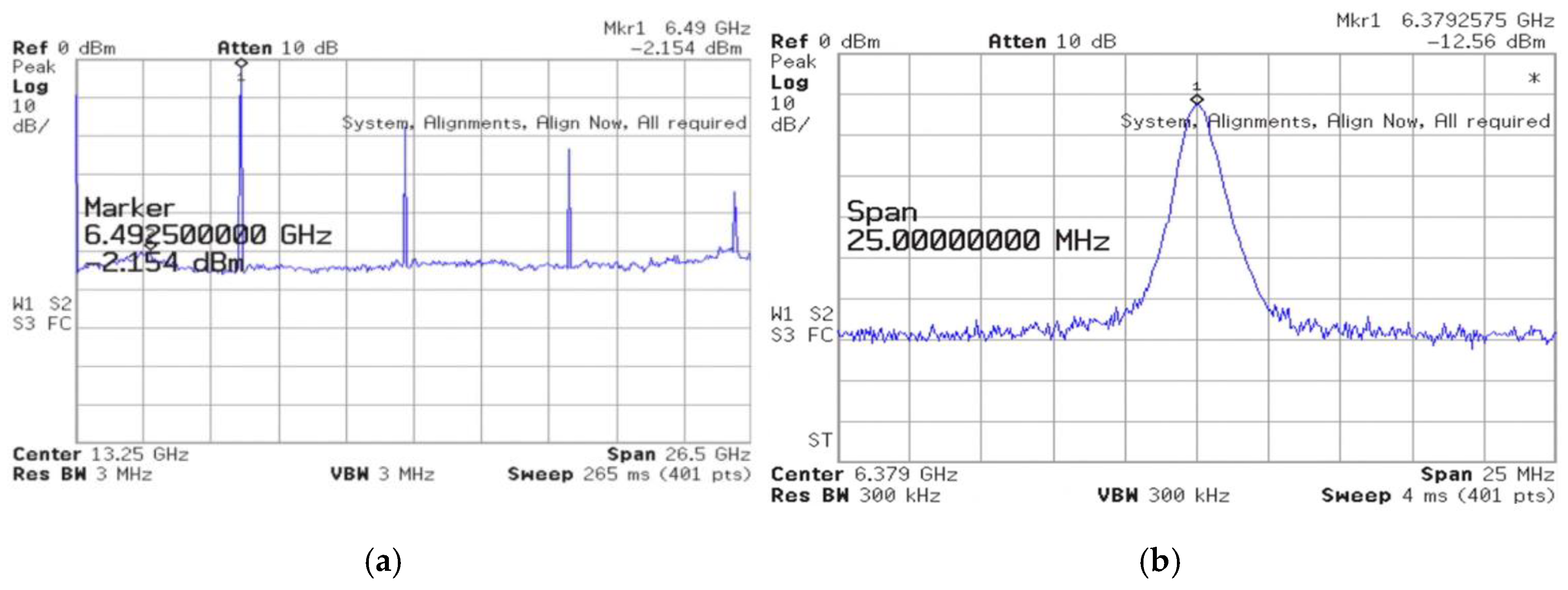
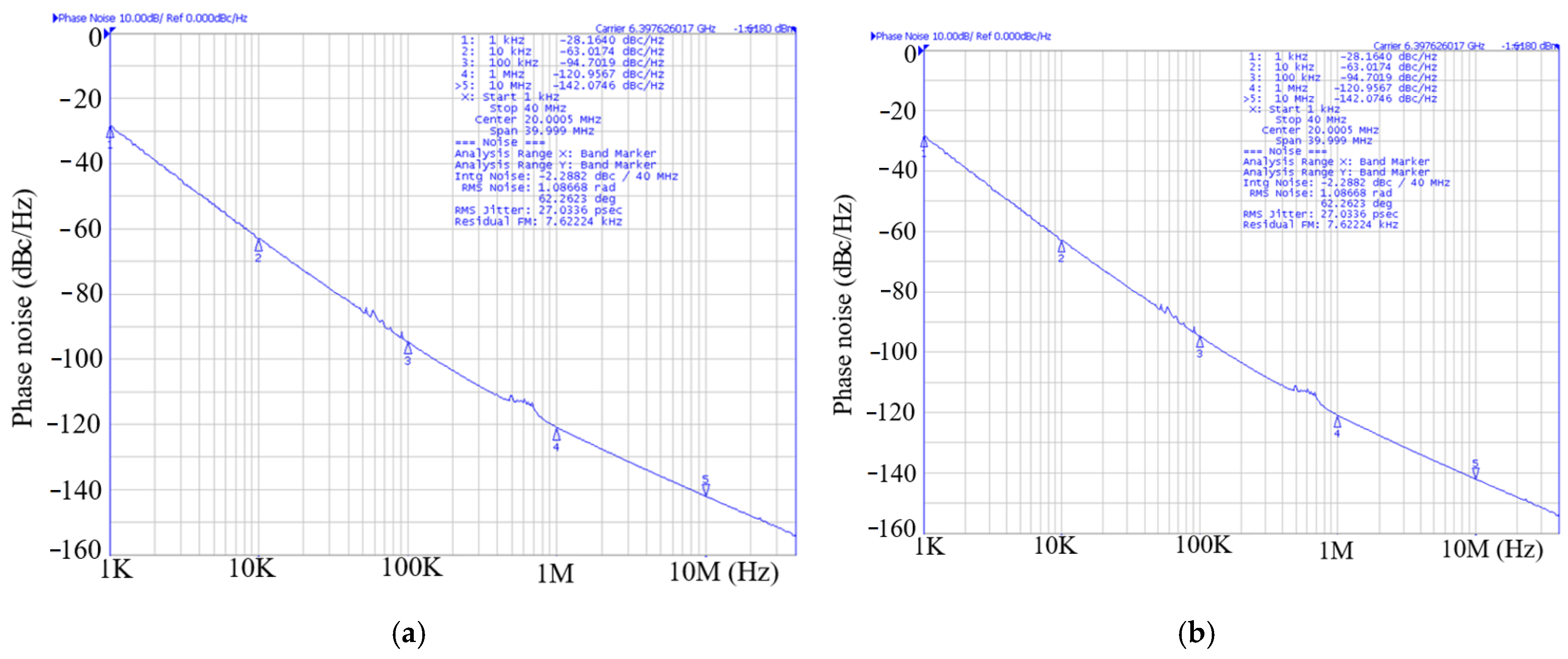
4.2. Measurement and Discussion

The 3rd FFO has been designed and fabricated in the WIN 0.12 μm GaN technology. The FFO was measured on the PC board. The measurements of oscillation frequency were conducted with the Keysight Spectrum Analyzer, while the phase noise was measured using the Keysight signal source analyzer. As shown in Figure 32, the die micrograph occupies an area of 0.8 × 0.8 mm2, including all test pads and dummy metal. Figure 33 shows the measured spectrum of the GaN FFO at 6.49 GHz. The carrier output power is −2.154 dBm. The second harmonic output power is −17.64 dBm, and the 3rd harmonic output power is −23.27 dBm. Figure 34a shows the measured phase noise of the FFO at VDD = 1 V. The phase noise at 1 MHz offset from the carrier at 6.397 GHz is −120.9 dBc/Hz. The corner frequency is 800 KHz. The FOM is −188.81 dBc/Hz. Figure 34b shows the measured phase noise of the FFO at VDD = 1.3 V. The phase noise at 1 MHz offset from the carrier at 6.397 GHz is −123.688 dBc/Hz. The corner frequency is 1 MHz. At 6.3971 GHz, the calculated FOM is −190.09 dBc/Hz. Similar to Figure 30a, Figure 35 shows the measured output voltages of the GaN FFO. Figure 33a resembles Figure 30b; the M1 and M2 cause the harmonic. Table 1 is the performance comparison of GaN oscillators.

5. Conclusions

This paper designs three GaN HEMT oscillators with a buffer. The oscillators include a single-ended oscillator, a balanced oscillator, and a cross-coupled oscillator. Two biases, oscillator supply and buffer supply, are used to optimize the oscillator performance and reliability of the circuit design. The first 8.86 GHz oscillator consists of an oscillator core biased at a supply voltage of 0.8 V and a buffer biased at 3 V. It can supply large output power because of a buffer biased at a high supply voltage, and it achieves low phase noise by operating the reliable oscillator core at a low supply voltage. The FoM of this oscillator is −199.8 dBc/Hz. We also study the hot-carrier stress effect on the 8.9 GHz GaN oscillator. When the core oscillator is subject to a supply voltage of 8 V, the post-bias oscillator phase noise measured at low supply voltage degrades. High FFO-core supply bias degrades the FOM. Biasing the oscillator core at low supply and the buffer at high supply is a good operation condition because high-oscillator FOM is maintained. The second 3.8 GHz balanced oscillator consists of two feedback sub-oscillators in a balanced configuration by suppressing the common mode oscillation, and the oscillator feedback uses a differential left-handed transmission line LC network for the first time in GaN HEMT oscillators. The balanced oscillator provides a differential signal, as verified by the time domain waveform. The output power increases and the phase noise improves with the supply voltage. For the present design, the output power can be controlled by buffer bias for higher output power. The oscillator phase noise degrades with high oscillator-core stress supply operation. The third 6.39 GHz C-band LC-tank oscillator with a buffer biased at high supply and the FFO-core biased at low supply is based on 0.12 μm WIN GaN-on-SiC technology. The oscillator uses 8-shaped inductors for suppressing magnetic coupling noise. At the supply of 1.3 V, the phase noise of the oscillator consists of 1/f2 and 1/f3 noise; the FFO FOM is −190.09 dBc/Hz. The FFO using two 1-turn 8-shaped inductors improves the oscillator phase noise by forming an intrinsic LC resonator to null the effect of the 2nd harmonic current on the phase noise.

Author Contributions

Investigation, C.-Y.H.; Investigation, T.C.Y.; Investigation, C.-T.L.; Writing—original draft, S.-L.J. All authors have read and agreed to the published version of the manuscript.

Funding

This research received no external funding.

Data Availability Statement

The original contributions presented in this study are included in the article. Further inquiries can be directed to the corresponding author.

Acknowledgments

The authors would like to thank the Staff of the TSRI for their help.

Conflicts of Interest

The authors declare no conflicts of interest.

References

  1. Balandin, A.; Morozov, S.V.; Cai, S.; Li, R.; Wang, K.L.; Wijeratne, G.; Viswanathan, C.R. Low flicker-noise GaN/AlGaN heterostructure field-effect transistors for microwave communications. IEEE Trans. Microw. Theory Tech. 1999, 47, 1413–1417. [Google Scholar] [CrossRef]
  2. Hörberg, M.; Kuylenstierna, D. Low phase noise power-efficient MMIC GaN-HEMT oscillator at 15 GHz based on a quasi-lumped on-chip resonator. In Proceedings of the 2015 IEEE MTT-S International Microwave Symposium, Phoenix, AZ, USA, 17–22 May 2015; pp. 1–4. [Google Scholar] [CrossRef]
  3. Jang, S.-L.; Chang, Y.-H.; Lai, W.-C. A Feedback GaN HEMT Oscillator. In Proceedings of the 2018 International Conference on Microwave and Millimeter Wave Technology (ICMMT), Chengdu, China, 7–11 May 2018; pp. 1–3. [Google Scholar] [CrossRef]
  4. Jang, L.; Chang, Y.-H.; Chiou, J.-S.; Lai, W.-C. A single GaN HEMT oscillator with 4-path inductors. In Proceedings of the IEEE ISNE-2018, Taipei, Taiwan, 7–9 May 2018. [Google Scholar]
  5. Herbert, Z.; Lai, S.; Dan, K.; Jonathan, F.; Kristoffer, A.; Niklas, R. An X-band low phase noise AlGaN-GaN-HEMT MMIC push-push oscillator. In Proceedings of the 2011 IEEE Compound Semiconductor Integrated Circuit Symposium (CSICS), Waikoloa, HI, USA, 16–19 October 2011; pp. 1–4. [Google Scholar]
  6. Lai, S.; Kuylenstierna, D.; Ozen, M.; Horberg, M.; Rorsman, N.; Angelov, I.; Zirath, H. Low phase noise GaN HEMT oscillators with excellent figures of merit. IEEE Microw. Wirel. Compon. Lett. 2014, 24, 412–414. [Google Scholar] [CrossRef]
  7. Wohlmuth, W.; Weng, M.-H.; Lin, C.-K.; Du, J.-H.; Ho, S.-Y.; Chou, T.-Y.; Li, S.M.; Huang, C.; Wang, W.-C.; Wang, W.-K. AlGaN/GaN HEMT development targeted for X band applications. In Proceedings of the 2013 IEEE International Conference on Microwaves, Communications, Antennas and Electronic Systems (COMCAS 2013), Tel Aviv, Israel, 21–23 October 2013; pp. 1–4. [Google Scholar]
  8. Jang, L.; Su, Y.-J.; Lin, K.J.; Wang, B.-J. An 4.7 GHz low power cross-coupled GaN HEMT oscillator. Microw. Opt. Technol. Lett. 2018, 60, 2442–2447. [Google Scholar] [CrossRef]
  9. Jang, S.-L.; Lin, K.J.; Lai, W.C.; Juang, M.-H. A capacitive cross-coupled GaN HEMT injection-locked frequency divider. In Proceedings of the 2018 International Symposium on VLSI Design, Automation and Test (VLSI-DAT), Hsinchu, Taiwan, 16–19 April 2018; pp. 1–3. [Google Scholar] [CrossRef]
  10. Sanabria, C.; Xu, H.; Heikman, S.; Mishra, U.K.; York, R.A. A GaN differential oscillator with improved harmonic performance. IEEE Microw. Wirel. Compon. Lett. 2005, 15, 463–465. [Google Scholar] [CrossRef]
  11. Soubercaze-Pun, G.; Tartarin, J.G.; Bary, L.; Rayssac, J.; Morvan, E.; Grimbert, B.; Delage, S.L.; De Jaeger, J.-C.; Graffeuil, J. Design of a X-band GaN oscillator: From the low frequency noise device characterization and large signal modeling to circuit design. In Proceedings of the 2006 IEEE MTT-S International Microwave Symposium Digest, San Francisco, CA, USA, 11–16 June 2006; pp. 747–750. [Google Scholar]
  12. Kaper, V.S.; Tilak, V.; Kim, H.; Vertiatchikh, A.V.; Thompson, R.M.; Prunty, T.R.; Eastman, L.F.; Shealy, J.R. High-power monolithic AlGaN/GaN HEMT oscillator. IEEE J. Solid State Circuits 2003, 38, 1457–1461. [Google Scholar] [CrossRef]
  13. Jang, S.-L.; Hou, J.C.; Shih, B.-S.; Li, G.-Z. Low-phase noise 8.22 GHz GaN HEMT oscillator using a feedback multi-path transformer. Microw. Opt. Technol. Lett. 2019, 61, 605–609. [Google Scholar] [CrossRef]
  14. Jang, S.-L.; Lin, H.-H.; Hsue, C.-W. Mode-switching left-handed standing wave voltage-controlled oscillator. Microw. Opt. Technol. Lett. 2013, 55, 1977–2244. [Google Scholar] [CrossRef]
  15. Jang, S.-L.; Lee, W.-H.; Hsue, C.-W. Fully-integrated standing wave oscillator using composite right/left-handed LC network. Microw. Opt. Technol. Lett. 2013, 55, 985–988. [Google Scholar] [CrossRef]
  16. Jang, S.-L.; Liu, Y.-W.; Chang, C.-W.; Hsue, C.-W. Dual-band VCO with composite right-/left-handed resonator. Microw. Opt. Technol. Lett. 2013, 55, 468–471. [Google Scholar] [CrossRef]
  17. Liu, H.; Zhu, X.; Boon, C.C.; Yi, X.; Mao, M.; Yang, W. Design of ultra-low phase noise and high power integrated oscillator in 0.25 µm GaN-on-SiC HEMT technology. IEEE Microw. Wirel. Compon. Lett. 2014, 24, 120–122. [Google Scholar] [CrossRef]
  18. Lai, S.; Kuylenstierna, D.; Hörberg, M.; Rorsman, N.; Angelov, I.; Andersson, K.; Zirath, H. Accurate phase-noise prediction for a balanced Colpitts GaN HEMT MMIC oscillator. IEEE Trans. Microw. Theory Tech. 2013, 61, 3916–3926. [Google Scholar] [CrossRef]
  19. Wang, J.; Huang, Y.; Chang, Y.-C.; Liu, Y.; Chang, D.C.; Hsu, S.S.H. A K-band MMIC cross-coupled oscillator with high output power in 0.25-μm GaN HEMT. IEEE Microw. Wirel. Techn. Lett. 2023, 33, 1211–1214. [Google Scholar] [CrossRef]
  20. Lee, S.; Jeon, S.; Jeong, J. Harmonic-tuned high-efficiency RF oscillator using GaN HEMTs. IEEE Microw. Wirel. Compon. Lett. 2012, 22, 318–320. [Google Scholar] [CrossRef]
  21. Jang, S.-L.; Lee, Y.-C.; Lai, W.-C. Left-Hand Resonator VCO Using an Orthogonal Transformer. Electronics 2025, 14, 2765. [Google Scholar] [CrossRef]
  22. Jang, S.-L.; Lin, Z.-J.; Juang, M.-H. State-of-the-Art VCO with eight-shaped resonator-type transmission line. Electronics 2025, 14, 2322. [Google Scholar] [CrossRef]
  23. Shahmohammadi, M.; Babaie, M.; Staszewski, R.B. A 1/f noise upconversion reduction technique for voltage-biased RF CMOS oscillators. IEEE J. Solid State Circuits 2016, 51, 2610–2624. [Google Scholar] [CrossRef]
Figure 1. (a) Block diagram of a feedback oscillator with an amplifier H. (b) Schematic and (c) equivalent circuit of the first HEMT oscillator.
Micromachines 16 00869 g001
Figure 2. Chip micrograph for the HEMT oscillator. 2 mm × 1 mm.
Micromachines 16 00869 g002
Figure 3. Measured I-V curve of buffer HEMT. Size: L = 0.25 μm, W = 75 μm, Number of fingers = 2.
Micromachines 16 00869 g003
Figure 4. Measured (a) expanded spectrum and (b) full-span spectrum. VDD = 0.8 V, VG1 = −2.4 V, VB = 3 V, and VG2 = −2 V.
Micromachines 16 00869 g004
Figure 5. Measured phase noise. VDD = 0.8 V, VG1 = −2.4 V, VB = 3 V, and VG2 = −2 V. A red 1/f 3 guideline is used for reference.
Micromachines 16 00869 g005
Figure 6. Measured output power and frequency versus VDD. VG1 = −2.4 V, VB = 3 V, and VG2 = −2 V.
Micromachines 16 00869 g006
Figure 7. Measured buffer bias effect. VDD = 0.8 V, VG1 = −2.4 V, VB = 0.8~4 V, and VG2 = −2 V.
Micromachines 16 00869 g007
Figure 8. FOM and FOMp versus VDD. VDD = 0.8~3 V, VG1 = −2.4 V, VB = 3 V, and VG2 = −2 V.
Micromachines 16 00869 g008
Figure 9. Measured oscillation frequency versus VDD. VB = 3 V, VG1 = −2.4, and VG2 = −2 V.
Micromachines 16 00869 g009
Figure 10. (a) Measured output power versus VDD. (b) Measured power consumption versus VDD. VB = 3 V, VG1 = −2.4, and VG2 = −2 V.
Micromachines 16 00869 g010
Figure 11. Measured phase noise versus step stress. (a) VDD = 0.8 V, VB = 3 V, VG1 = −2.4, and VG2 = −2 V. Measured on chip 1. (b) VDD = 1 V, VB = 3 V, VG1 = −2.4, VG2 = −2 V. (c) VDD = 3 V, VB = 3 V, VG1 = −2.4, and VG2 = −2 V.
Micromachines 16 00869 g011
Figure 12. Measured phase noise at 1 MHz offset frequency versus VDD. VB = 3 V, VG1 = −2.4, and VG2 = −2 V. Measured on chip 1.
Micromachines 16 00869 g012
Figure 13. Calculated FOM. VB = 3 V, VG1 = −2.4, and VG2 = −2 V. Measured on chip 1.
Micromachines 16 00869 g013
Figure 14. (a) Measured fresh and stressed I-V of buffer FET versus VB. Measured on chip 2. VG2 = −1, −2, and −3 V. Blue: fresh, and red: post-stress. (b). Measured oscillation frequency versus VB. VDD = 0.75 V, VG1 = −2.4, and VG2 = −2 V. Measured on chip 2. (c) Measured phase noise versus step stress. VDD = 0.75 V, VB = 2 V, VG1 = −2.4, and VG2 = −2 V. Measured on chip 2.
Micromachines 16 00869 g014
Figure 15. (a) Right-handed T-lines and (b) left-handed T-lines.
Micromachines 16 00869 g015
Figure 16. Schematic (a) and equivalent circuit (b) of the second oscillator.
Micromachines 16 00869 g016
Figure 17. (a) Simulated input impedance at the drain of M1. VDD = 2 V, VG1 = −2 V, VB = 2 V, and VG2 = −2 V. (b) Simulated inductance and Q-factor of inductor L1 (= L2 = L3).
Micromachines 16 00869 g017
Figure 18. Chip micrograph for the HEMT oscillator. 2 mm × 1 mm.
Micromachines 16 00869 g018
Figure 19. Measured output voltages. VDD = 0.6 V, VG1 = −2.1 V, VB = 0.8 V, and VG2 = −2.1 V.
Micromachines 16 00869 g019
Figure 20. Measured spectrum. VDD = 1.4 V, VG1 = −2.2 V, VB = 0.8 V, and VG2 = −2.3 V.
Micromachines 16 00869 g020
Figure 21. Measured phase noise. VDD = 0.6–2 V, VG1 = −2.1 V, VB = 0.8 V, and VG2 = −2.1 V. The green line is used as a guideline for phase noise due to thermal noise.
Micromachines 16 00869 g021
Figure 22. Measured frequency, phase noise, output power, and current consumption vs. VDD. VDD = 0.6~2 V, VG1 = −2.2 V, VB = 0.8 V, and VG2 = −2.3 V.
Micromachines 16 00869 g022
Figure 23. Measured power consumption and output power of the buffer versus VB. VDD = 1.4 V, VG1 = −2.1 V, VB = 0.2 ~ 2 V, and VG2 = −2.3 V.
Micromachines 16 00869 g023
Figure 24. Measured output power, oscillation frequency, and core current consumption versus biased time. VDD = 15 V, VG1= −2.1 V, VB = 0.8 V, and VG2 = −2.1 V.
Micromachines 16 00869 g024
Figure 25. (a) Measured phase noises for tbias = 0, 30, 60 min. VDD = 0.6 V, VG1 = −2.1 V, VB = 0.8 V, and VG2 = −2.1 V. (b) Measured post-stress phase noises at 1 MHz offset frequency. VDD = 0.6–2 V, VG1 = −2.1 V, VB = 0.8 V, and VG2 = −2.1 V.
Micromachines 16 00869 g025
Figure 26. Circuit schematic of the third designed GaN FFO.
Micromachines 16 00869 g026
Figure 27. Equivalent circuit for the dual resonant network.
Micromachines 16 00869 g027
Figure 28. (a) Simulated phase noise. Red: deleted (L2, L3). (b) Impedances between A and B nodes. Purple/Red tank impedance with/without (L2, L3). Blue impedance between C and D nodes.
Micromachines 16 00869 g028
Figure 29. Simulated waveforms and frequency-domain analysis of the oscillator: (a) drain (VD) and gate (VG) voltage waveforms of transistor M1; (b) drain current (ID) waveform of transistor M1; (c) DFT results of drain voltage (VD), drain current (ID), and impedance magnitude between nodes A and B.
Micromachines 16 00869 g029
Figure 30. Simulated drain voltage Vout1 waveform (a,b), DFT analysis of voltage (VC) and current (IC) at node C, and the impedance magnitude between nodes C and D (ZCD), based on the oscillator schematic in Figure 26. VDD = 1.3 V, Vbias = −1.6 V, VDB = 5 V, and VB = −2 V.
Micromachines 16 00869 g030
Figure 31. (a) Layout of L2. (b) Layout of L1. (c) Simulated inductance and Q-factor.
Micromachines 16 00869 g031
Figure 32. Chip photo of FFO.
Micromachines 16 00869 g032
Figure 33. Measured (a) full-span spectrum and (b) expanded spectrum of the VCO. VDD = 1.3 V, Vbias = −1.6 V, VDB = 5 V, and VB = −2 V.
Micromachines 16 00869 g033
Figure 34. (a) Measured phase noise of the GaN FFO. VDD = 1 V, Vbias= −1.6 V, VDB = 5 V, and VB = −2 V. (b). Measured phase noise of the GaN FFO. VDD = 1.3 V, Vbias = −1.6 V, VDB = 5 V, and VB = −2 V.
Micromachines 16 00869 g034
Figure 35. Measured output voltages of the GaN FFO. VDD = 1.3 V, VDB = 5 V, VB = −2 V, and Vbias = −1.6 V.
Micromachines 16 00869 g035
Table 1. Performance comparison of GaN oscillators.
RefProc (um)TopolVdd (V)/
Pdis (mW)
fo
GHz
PN dBc/HzFOM
dBc/Hz
8-Shaped
Inductor
[7]0.25Hartley28/14567.9−112 *−178no
[10]0.25Balanced Colpitts6/1809.92−136−193no
[14]-Push-push15/6009.1−130−181no
[15]0.25Common source10/6009.9−135−187no
[16]0.25Common gate30/106259.55−115.0−154.0no
[17]0.25Cross-coup0.4/2.6694.746−121.77−191.03no
[18]0.25Bal Colpitts Osc15/6008.6−102−172.9no
[19]0.25Cross-Coupled VCO-/74723.9–24.4−109.4−168.3no
[20]-Osc (on-board)28/4.92.44−123.1−164.03no
This 10.25feedback0.8/2.458.86−124.8−199.8no
This 20.25LH feedback1.6/31.363.818−131.73−188.4no
This 30.12Cross-Coupled Osc1.3/9.3736.397−123.688−190.09yes
* @100 KHz. 1 chip in Figure 2. 2 chip in Figure 18. 3 chip in Figure 32.
Disclaimer/Publisher’s Note: The statements, opinions and data contained in all publications are solely those of the individual author(s) and contributor(s) and not of MDPI and/or the editor(s). MDPI and/or the editor(s) disclaim responsibility for any injury to people or property resulting from any ideas, methods, instructions or products referred to in the content.

