

Design and Analysis of Ultra-Thin Broadband Transparent Absorber Based on ITO Film


Abstract
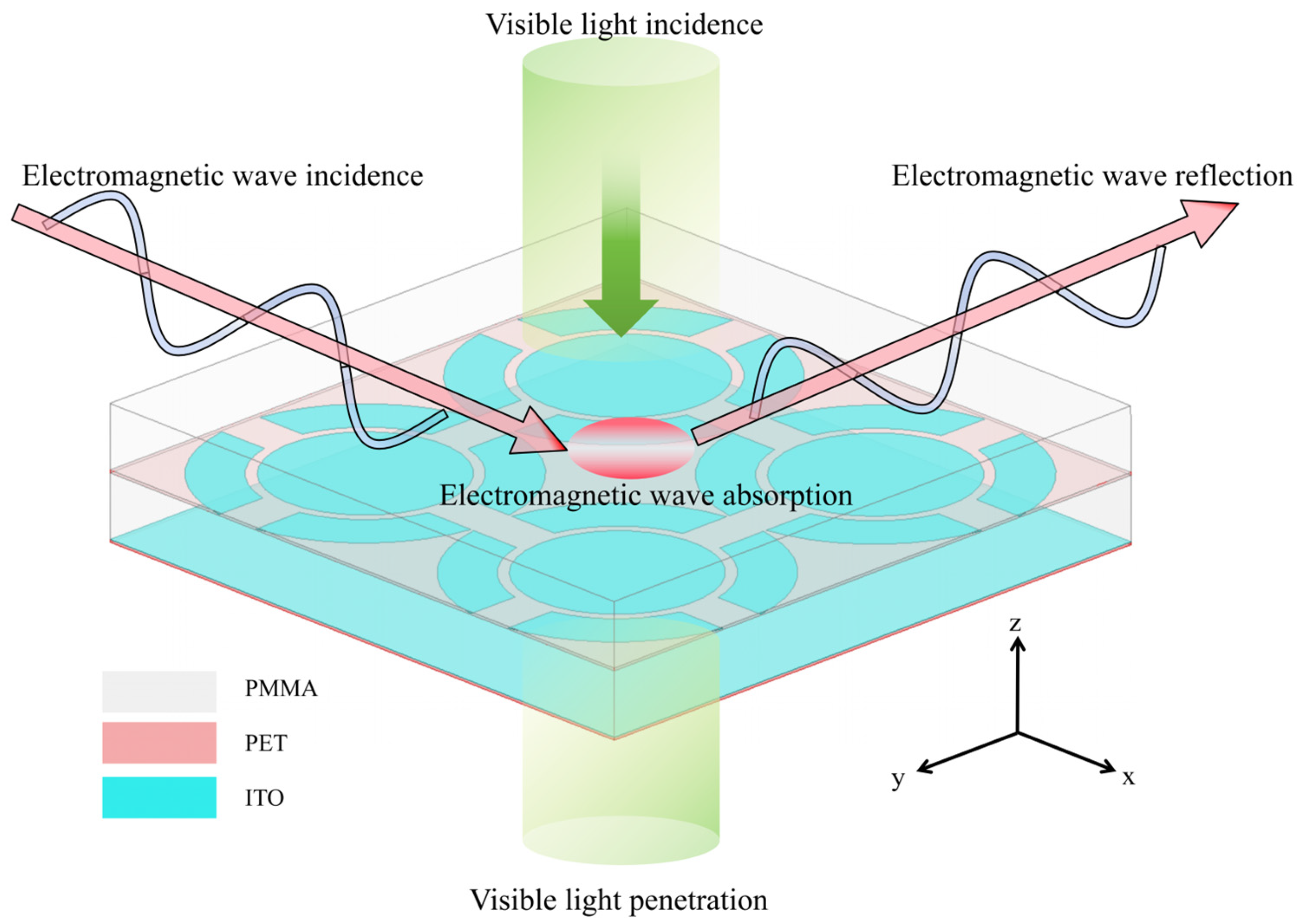
1. Introduction
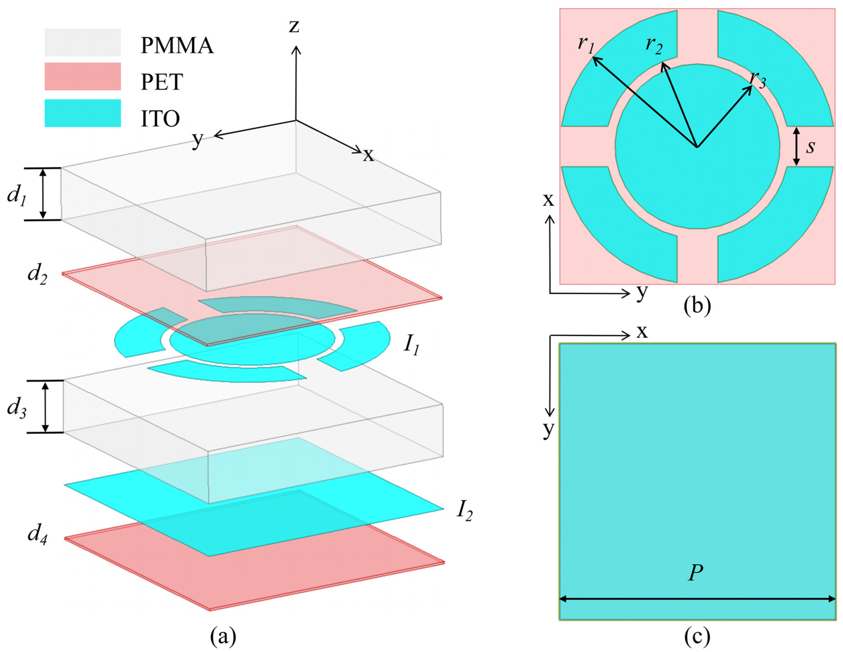
2. Design and Analysis
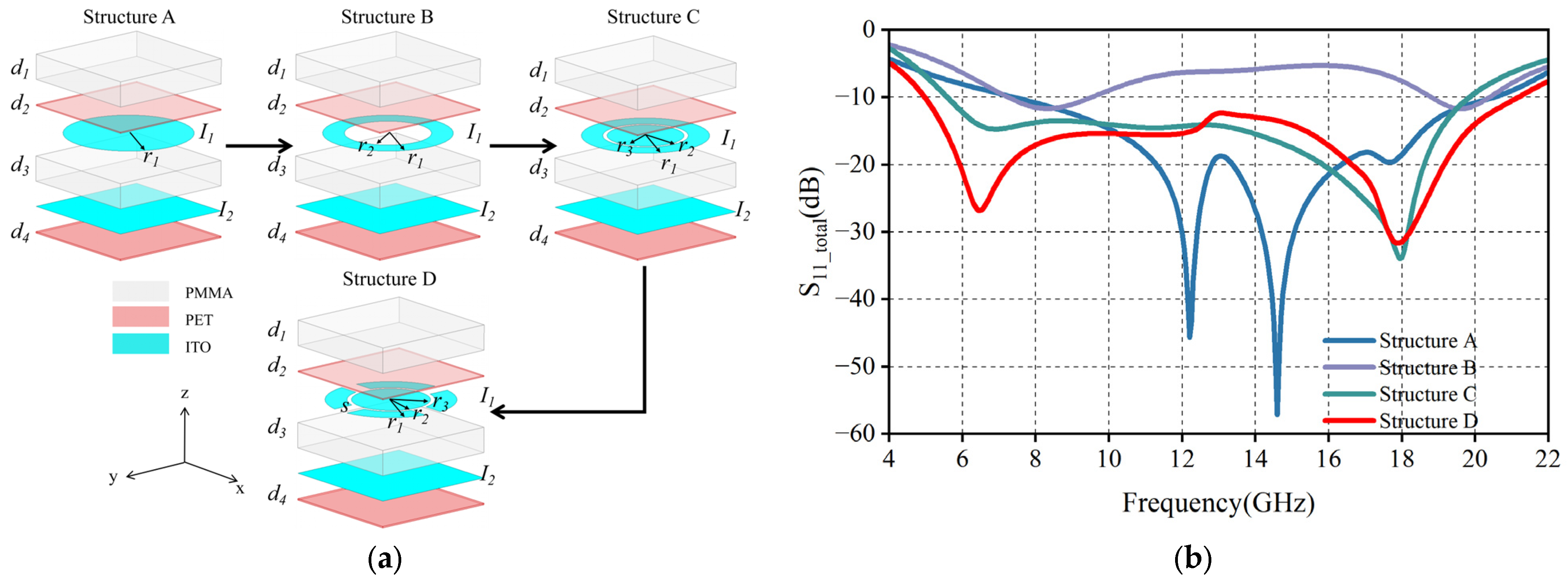
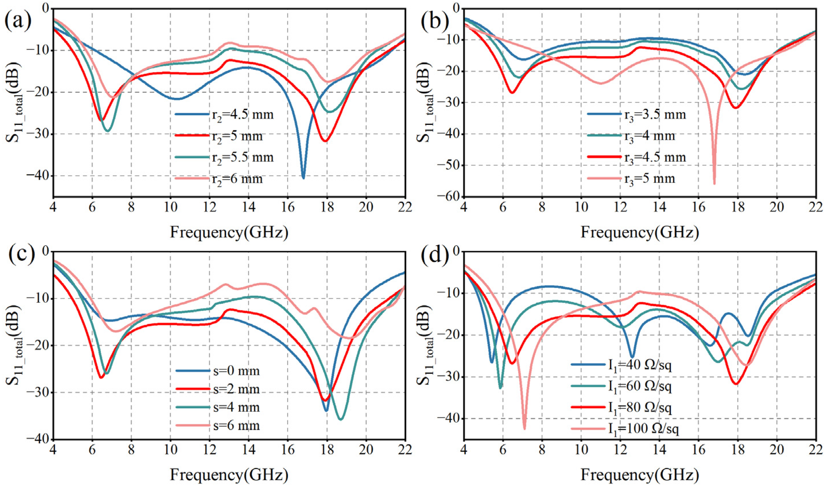
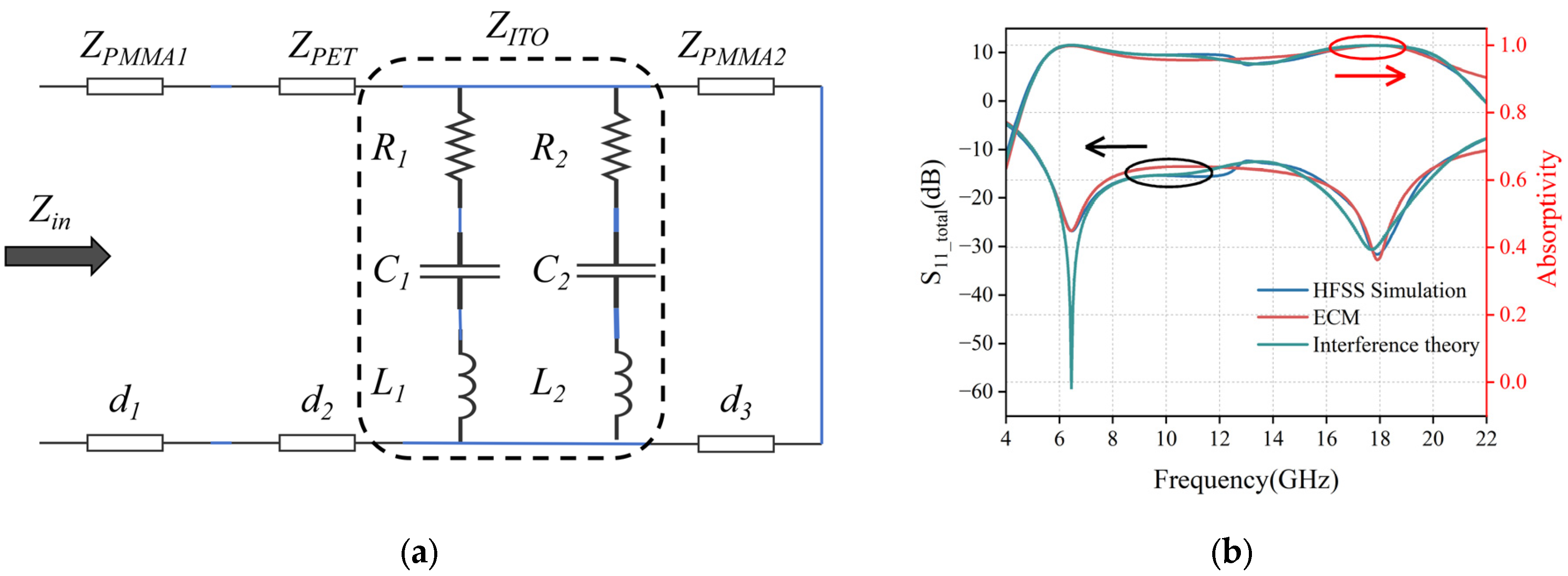
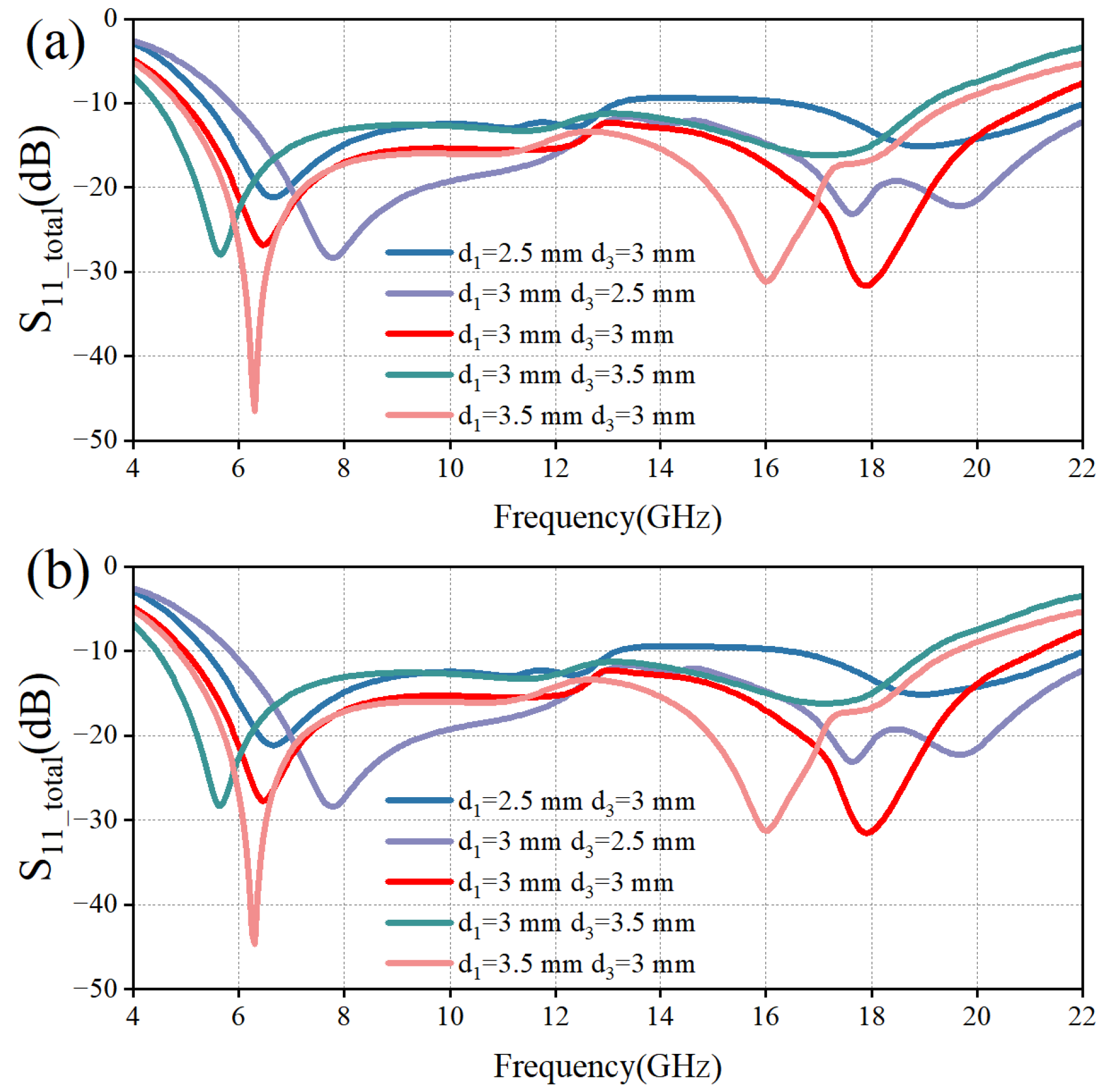
2.1. Modular Design
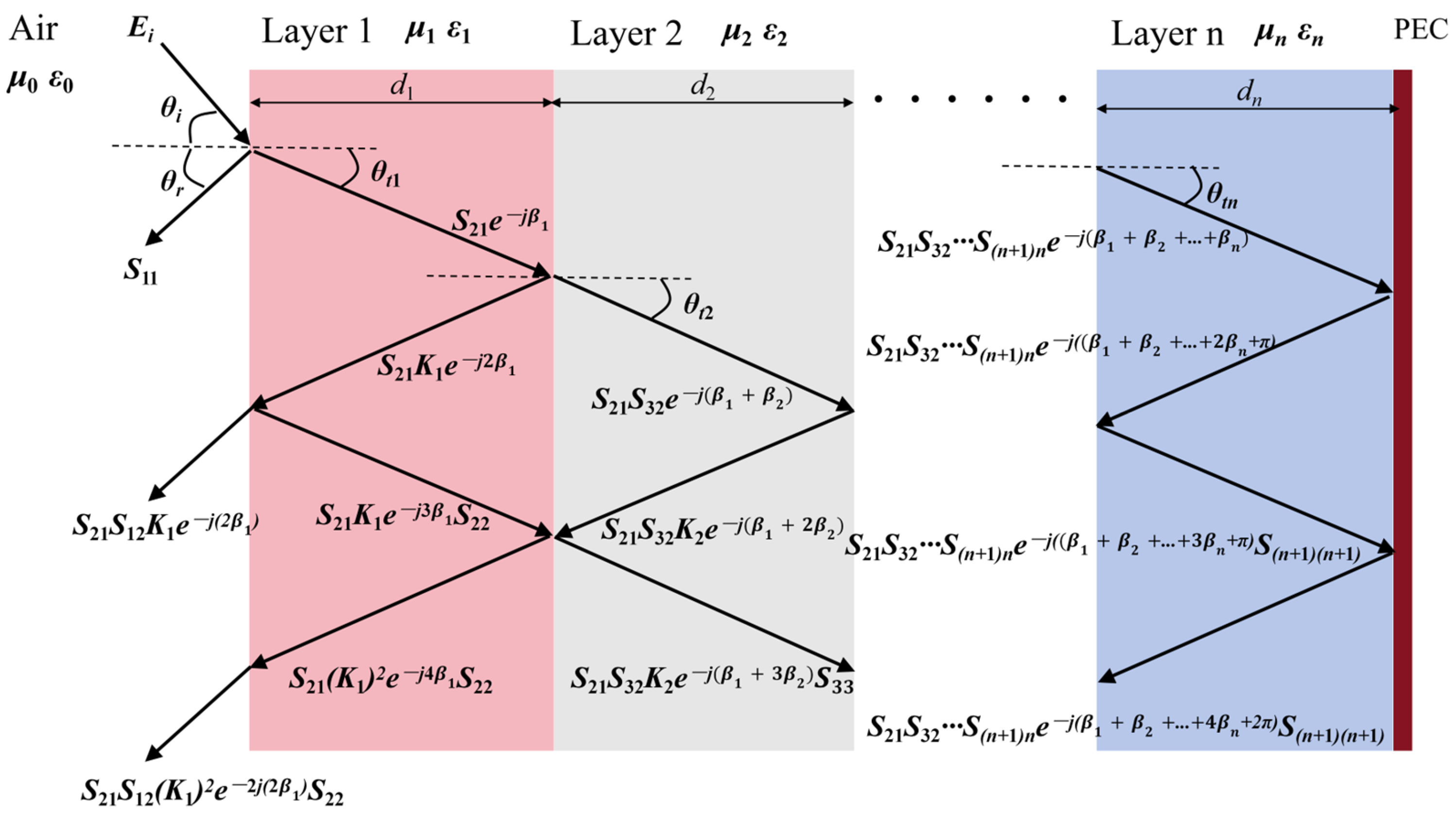
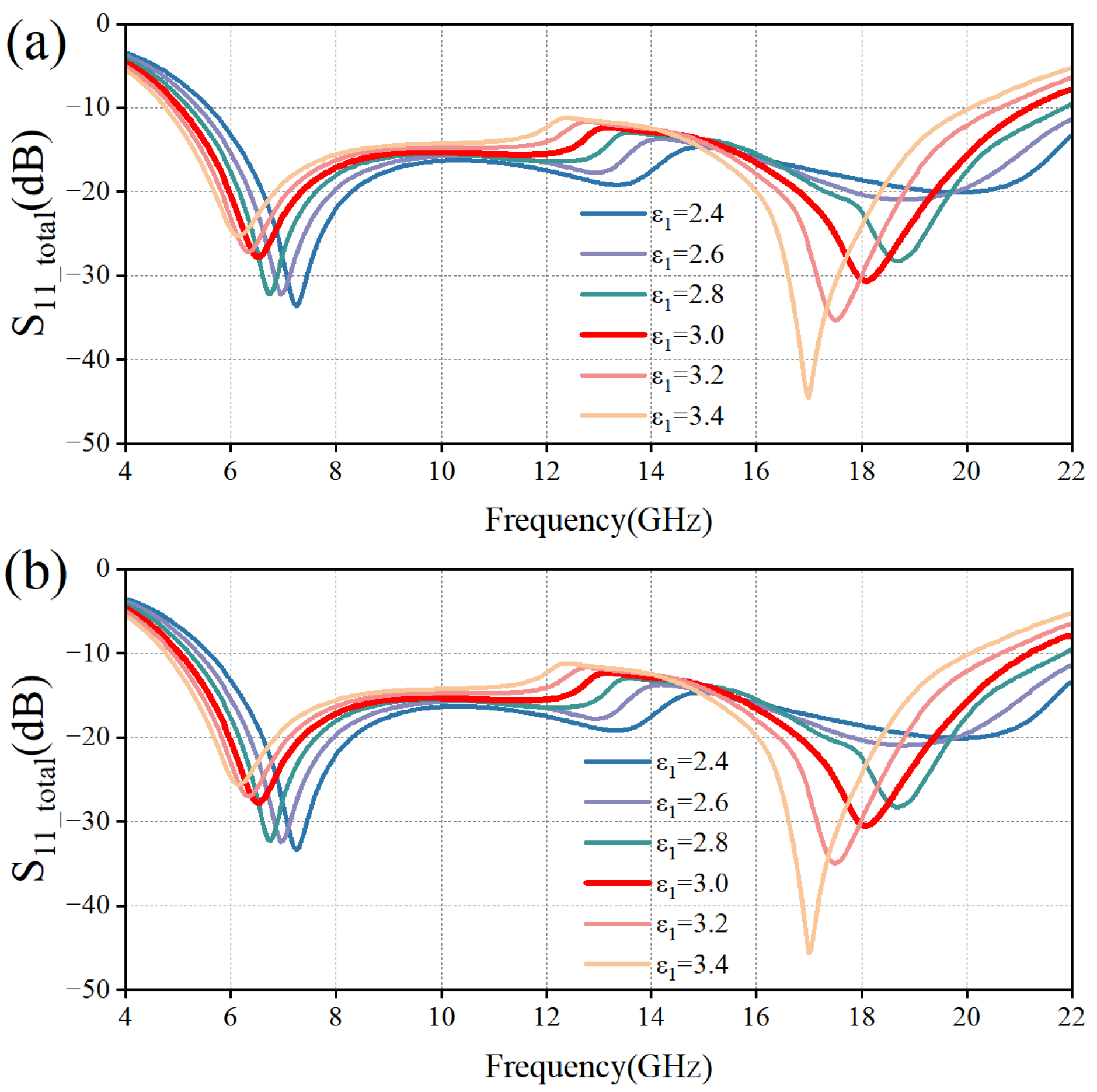
2.2. Interference Theory Analysis
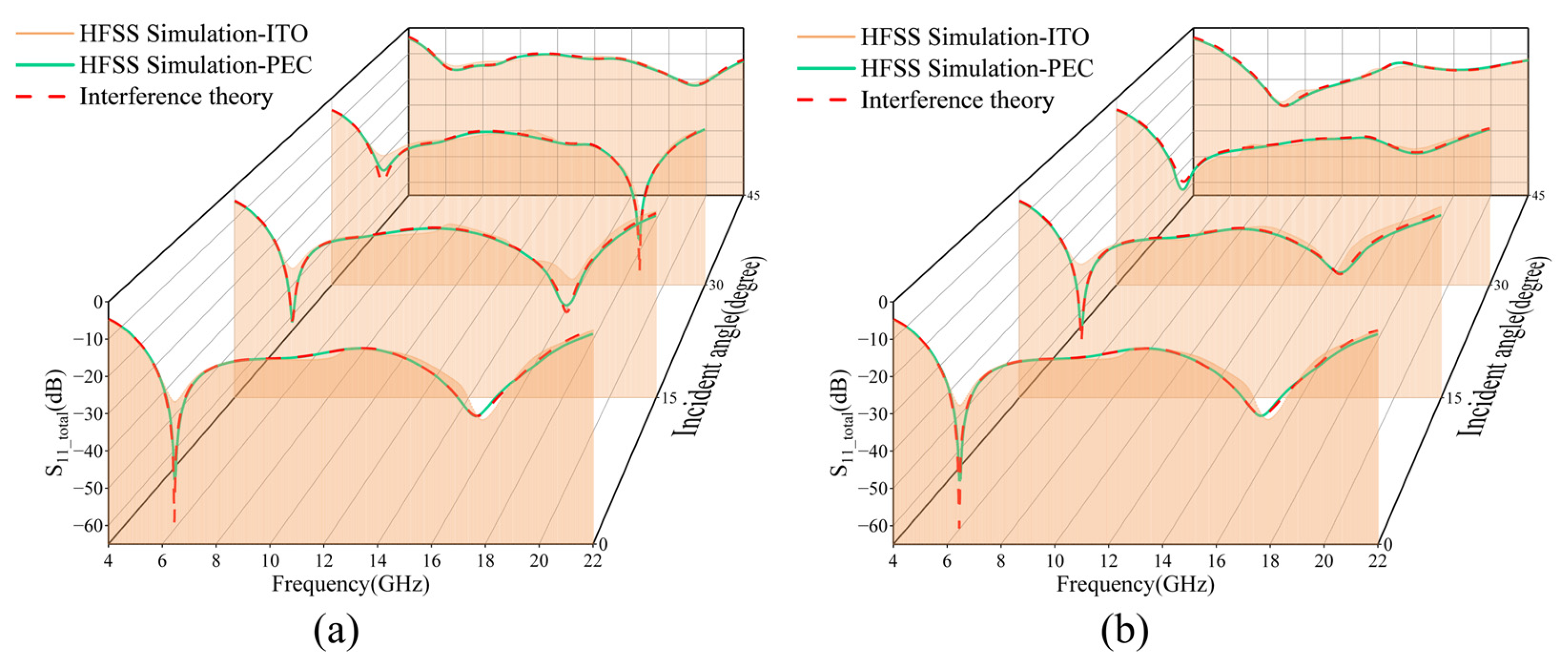
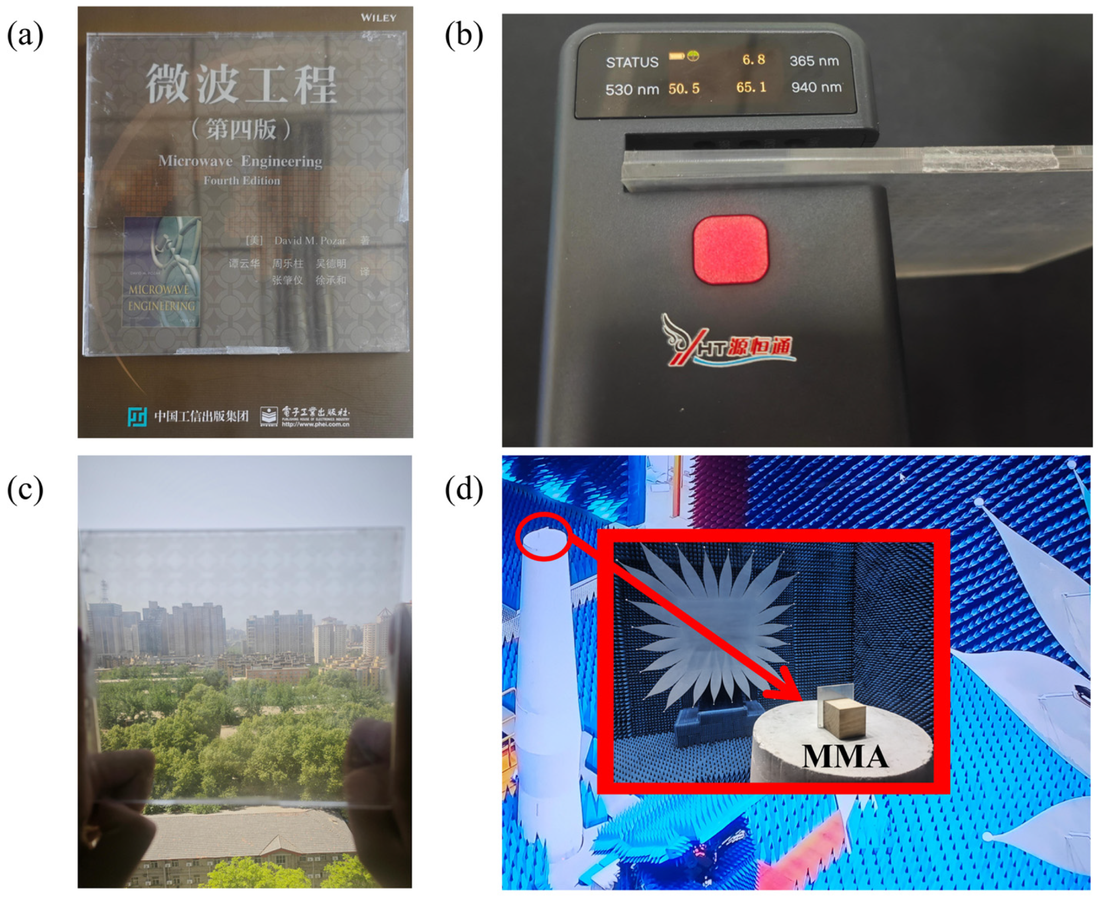
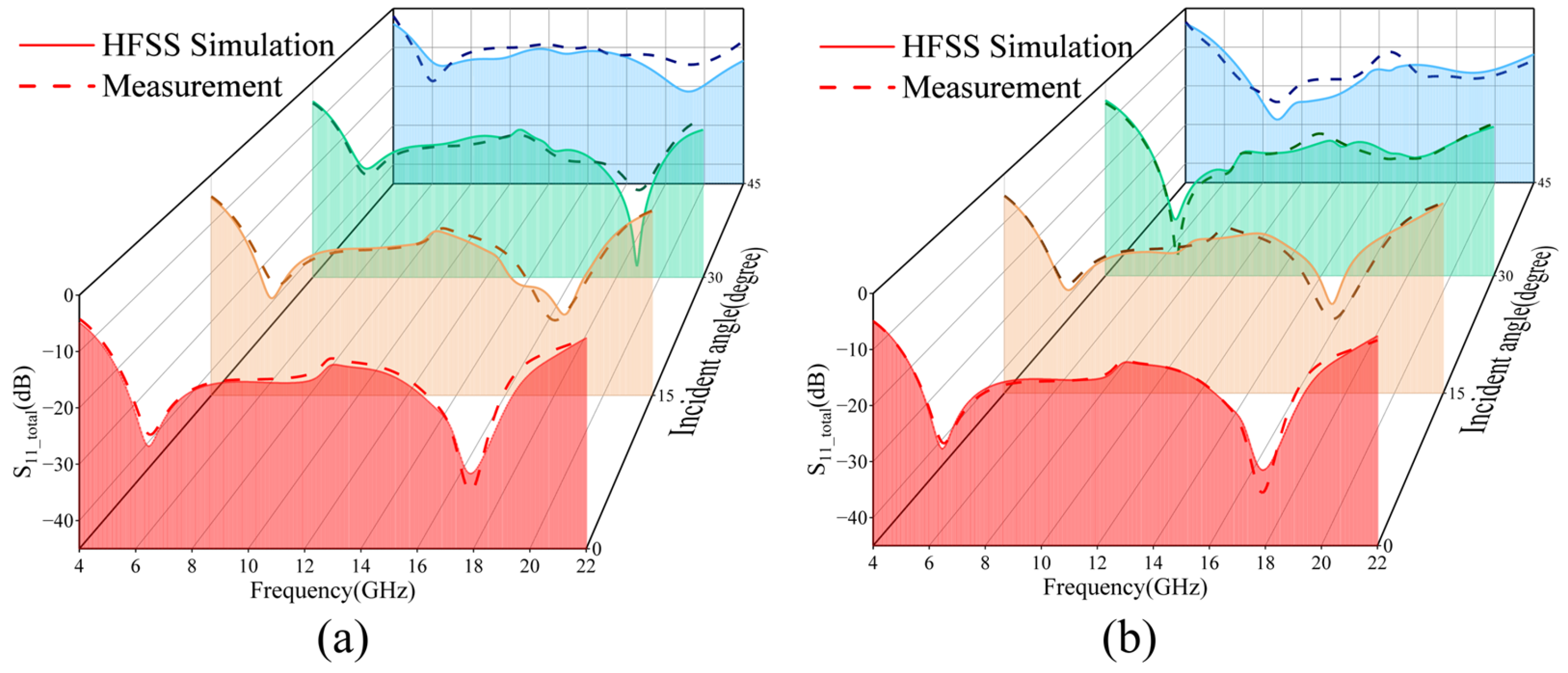
3. Experimental Verification
4. Conclusions
Author Contributions
Funding
Data Availability Statement
Conflicts of Interest
References
- Fionov, A.; Kraev, I.; Yurkov, G.; Solodilov, V.; Zhukov, A.; Surgay, A.; Kuznetsova, I.; Kolesov, V. Radio-Absorbing Materials Based on Polymer Composites and Their Application to Solving the Problems of Electromagnetic Compatibility. Polymers 2022, 14, 3026. [Google Scholar] [CrossRef] [PubMed]
- Hossain, M.B.; Faruque, M.R.I.; Abdullah, S.; Islam, M.T.; Al-mugren, K.S. A Coding Based Metasurface Absorber with Triple Circular Ring Resonator for Broadband RCS Reduction and High EMI Shielding Effectiveness. Results Eng. 2024, 21, 101791. [Google Scholar] [CrossRef]
- Zheng, L.; Zuo, Y.; Song, D.; Li, X.; Lou, Z.; Wu, Y. Green Strategy for a Large-Format, Superhard, and Insulated Electromagnetic Wave Absorber Inspired by a Natural Feature of a Conch Shell. ACS Nano 2024, 18, 29457–29468. [Google Scholar] [CrossRef]
- Pang, H.; Duan, Y.; Huang, L.; Song, L.; Liu, J.; Zhang, T.; Yang, X.; Liu, J.; Ma, X.; Di, J.; et al. Research Advances in Composition, Structure and Mechanisms of Microwave Absorbing Materials. Compos. Part B Eng. 2021, 224, 109173. [Google Scholar] [CrossRef]
- Si, T.; Xie, S.; Ji, Z.; Ma, C.; Wu, Z.; Wu, J.; Wang, J. Modification of Basalt Fiber with Ni and Carbon Black Formed Synergistic Microstructure for Enhanced Electromagnetic Wave Absorption. J. Mater. Sci. Mater. Electron. 2023, 34, 1035. [Google Scholar] [CrossRef]
- Xie, A.; Ma, Z.; Xiong, Z.; Li, W.; Jiang, L.; Zhuang, Q.; Cheng, S.; Lu, W. Conjugate Ferrocene Polymer Derived Magnetic Fe/C Nanocomposites for Electromagnetic Absorption Application. J. Mater. Sci. Technol. 2024, 175, 125–131. [Google Scholar] [CrossRef]
- Javed, Z.; Rasool, R.T.; Alhummiany, H.; Majeed, A.; Gulbadan, S.; Ashraf, G.A.; Al-Anazy, M.M.; Irfan, M.; Yousef, E.S.; Akhtar, M.N.; et al. Structural, Morphological, Dielectric, and Spectral Properties of Sr-Mg-Ho X-Type Magnetic Nanomaterials Suitable for Microwave Absorption Application. Vacuum 2024, 222, 112965. [Google Scholar] [CrossRef]
- Feng, J.; Wu, L.-S.; Mao, J.-F. Switchable Broadband/Narrowband Absorber Based on a Hybrid Metasurface of Graphene and Metal Structures. Opt. Express 2023, 31, 12220–12231. [Google Scholar] [CrossRef]
- Tao, G.; Zhao, Q.; Song, Q.; Yi, Z.; Yi, Y.; Zeng, Q. A Polarization-Insensitive and Highly Sensitive THz Metamaterial Multi-Band Perfect Absorber. Micromachines 2024, 15, 1388. [Google Scholar] [CrossRef]
- Zhang, Y.; Gao, Y.; Yang, S.; Li, Z.; Wang, X.; Zhang, J. Modeling of a Broadband Microwave Composite Thin Film Absorber. Micromachines 2023, 14, 2119. [Google Scholar] [CrossRef]
- Landy, N.I.; Sajuyigbe, S.; Mock, J.J.; Smith, D.R.; Padilla, W.J. Perfect Metamaterial Absorber. Phys. Rev. Lett. 2008, 100, 207402. [Google Scholar] [CrossRef] [PubMed]
- Zadeh, A.K.; Karlsson, A. Capacitive Circuit Method for Fast and Efficient Design of Wideband Radar Absorbers. IEEE Trans. Antennas Propag. 2009, 57, 2307–2314. [Google Scholar] [CrossRef]
- Xie, J.; Quader, S.; Xiao, F.; He, C.; Liang, X.; Geng, J.; Jin, R.; Zhu, W.; Rukhlenko, I.D. Truly All-Dielectric Ultrabroadband Metamaterial Absorber: Water-Based and Ground-Free. IEEE Antennas Wirel. Propag. Lett. 2019, 18, 536–540. [Google Scholar] [CrossRef]
- Huo, P.; Zhang, C.; Zhu, W.; Liu, M.; Zhang, S.; Zhang, S.; Chen, L.; Lezec, H.J.; Agrawal, A.; Lu, Y.; et al. Photonic Spin-Multiplexing Metasurface for Switchable Spiral Phase Contrast Imaging. Nano Lett. 2020, 20, 2791–2798. [Google Scholar] [CrossRef]
- Zheng, C.-L.; Ni, P.-N.; Xie, Y.-Y.; Genevet, P. On-Chip Light Control of Semiconductor Optoelectronic Devices Using Integrated Metasurfaces. Opto-Electron. Adv. 2025, 8, 240159. [Google Scholar] [CrossRef]
- Zang, H.; Zhou, X.; Yang, Z.; Yu, Q.; Zheng, C.; Yao, J. Polarization Multiplexed Multifunctional Metasurface for Generating Longitudinally Evolving Vector Vortex Beams. Phys. Lett. A 2024, 497, 129336. [Google Scholar] [CrossRef]
- Zhong, S.; Zhang, Y.; Ma, Y. Optically Transparent Frequency-Tunable Microwave Absorber Based on Patterned Graphene-ITO Structure. IEEE Trans. Antennas Propag. 2022, 70, 9959–9964. [Google Scholar] [CrossRef]
- Xi, Y.; Jiang, W.; Wei, K.; Hong, T.; Gong, S. An Optically Transparent Hybrid Mechanism Metasurface for Wideband, Wide-Angle and Omnidirectional Scattering Suppression. IEEE Trans. Antennas Propag. 2023, 71, 422–432. [Google Scholar] [CrossRef]
- Hu, X.; Wang, Y.; Wan, Z.; Li, Y.; Li, R.; Li, H.; Cao, Q. Design and Analysis of an Optically Transparent Ultra-Wideband Absorber Covering C-, X-, Ku-, K-, Ka- Bands. Opt. Mater. Express 2022, 12, 1512–1521. [Google Scholar] [CrossRef]
- Dai, H.; Li, S.; Dong, P.; Ma, Y. Design of an Ultra-Wideband Transparent Wave Absorber. Materials 2023, 16, 5962. [Google Scholar] [CrossRef]
- Hayat, B.; Zhang, J.; Khan, A.; Abbas, S.M.; Majeed, A.; Al-Bawri, S.S. A Flexible and Optical Transparent Metasurface Absorber with Broadband RCS Reduction Characteristics. Nanomaterials 2024, 14, 1507. [Google Scholar] [CrossRef] [PubMed]
- Xiong, Y.; Chen, F.; Cheng, Y.; Luo, H. Ultra-Thin Optically Transparent Broadband Microwave Metamaterial Absorber Based on Indium Tin Oxide. Opt. Mater. 2022, 132, 112745. [Google Scholar] [CrossRef]
- Dong, L.; Si, L.; Xu, H.; Shen, Q.; Lv, X.; Zhuang, Y.; Zhang, Q. Rapid Customized Design of a Conformal Optical Transparent Metamaterial Absorber Based on the Circuit Analog Optimization Method. Opt. Express 2022, 30, 8303–8316. [Google Scholar] [CrossRef] [PubMed]
- Lai, S.; Liu, Y.; Luo, J. Flexible and Transparent Broadband Absorber Based on Gridded ITO Ground. IEEE Photon. Technol. Lett. 2024, 36, 223–226. [Google Scholar] [CrossRef]
- Chen, J.; Hu, Z.; Wang, G.; Huang, X.; Wang, S.; Hu, X.; Liu, M. High-Impedance Surface-Based Broadband Absorbers with Interference Theory. IEEE Trans. Antennas Propag. 2015, 63, 4367–4374. [Google Scholar] [CrossRef]
- Wanghuang, T.; Chen, W.; Huang, Y.; Wen, G. Analysis of Metamaterial Absorber in Normal and Oblique Incidence by Using Interference Theory. AIP Adv. 2013, 3, 102118. [Google Scholar] [CrossRef]
- Chen, H.-T. Interference Theory of Metamaterial Perfect Absorbers. Opt. Express 2012, 20, 7165–7172. [Google Scholar] [CrossRef]
- Zeng, X.; Gao, M.; Zhang, L.; Wan, G.; Hu, B. Design of a Triple-Band Metamaterial Absorber Using Equivalent Circuit Model and Interference Theory. Microw. Opt. Technol. Lett. 2018, 60, 1676–1681. [Google Scholar] [CrossRef]
- Zhiying, C.; Yueming, G.; Min, D. Electromagnetic Wave Transmission Characteristics on Different Tissue Boundaries for Implantable Human Body Communication. Chin. J. Radio Sci. 2017, 32, 134–143. [Google Scholar]
- Han, Y.; Zhu, L.; Chang, Y.; Li, B. Dual-Polarized Bandpass and Band-Notched Frequency-Selective Absorbers Under Multimode Resonance. IEEE Trans. Antennas Propag. 2018, 66, 7449–7454. [Google Scholar] [CrossRef]
- Ji, Z.; Song, Y.; Gao, M.; Zhang, Q.; Liu, Y. Multimode Miniature Polarization-Sensitive Metamaterial Absorber with Ultra-Wide Bandwidth in the K Band. Micromachines 2024, 15, 1446. [Google Scholar] [CrossRef] [PubMed]
- Ji, S.; Ren, H.; Zhang, C.; Zhao, J.; Wu, H.; Dai, H. Optically Transparent Conformal Ultra-Broadband Metamaterial Absorber Based on ITO Conductive Film. J. Phys. D Appl. Phys. 2023, 56, 425101. [Google Scholar] [CrossRef]
- Li, T.; Chen, K.; Ding, G.; Zhao, J.; Jiang, T.; Feng, Y. Optically Transparent Metasurface Salisbury Screen with Wideband Microwave Absorption. Opt. Express 2018, 26, 34384–34395. [Google Scholar] [CrossRef]
- Zhou, Q.; Yin, X.; Ye, F.; Mo, R.; Tang, Z.; Fan, X.; Cheng, L.; Zhang, L. Optically Transparent and Flexible Broadband Microwave Metamaterial Absorber with Sandwich Structure. Appl. Phys. A 2019, 125, 131. [Google Scholar] [CrossRef]
- Bhardwaj, A.; Singh, G.; Srivastava, K.V.; Ramkumar, J.; Ramakrishna, S.A. Polarization-Insensitive Optically Transparent Microwave Metamaterial Absorber Using a Complementary Layer. IEEE Antennas Wirel. Propag. Lett. 2022, 21, 163–167. [Google Scholar] [CrossRef]


| Symbol | Explanation |
|---|---|
| S(n−1)(n−1) | The partial reflection coefficient of the wave from the (n − 1)-th layer when it is incident on the surface of the nth layer of the medium data |
| Snn | The partial reflection coefficient of the wave from the nth layer when it is incident on the surface of the (n − 1)-th layer of the medium |
| Sn(n−1) | The partial transmission coefficient of a wave from the (n − 1)-th layer incident on the nth layer of the medium |
| S(n−1)n | The partial transmission coefficient of a wave from the nth layer incident on the (n − 1)-th layer of the medium |
| Document | Bandwidth (GHz) | FBW (%) | Structure Thickness | Angle Absorption | Transparency | |
|---|---|---|---|---|---|---|
| TM | TE | |||||
| [30] | 2.03–6.98 | 109.9 | 0.08λL (12 mm) | ~45° | ~45° | No |
| [31] | 20.76–24.2 | 15.3 | 0.109λL (1.575 mm) | ~30° | ~15° | No |
| [32] | 6.54–18.66 | 96.2 | 0.117λL (5.35 mm) | ~50° | ~50° | Yes |
| [33] | 4.1–17.5 | 124 | 0.095λL (7 mm) | ~40° | ~40° | Yes |
| [34] | 8–18 | 76.9 | 0.12λL (4.5 mm) | ~30° | ~30° | Yes |
| [35] | 2–4.5 | 76.9 | 0.0847λL (12.7 mm) | ~30° | ~40° | Yes |
| This work | 5–21.15 | 123.5 | 0.105λL (6.3 mm) | ~45° | ~45° | Yes |
Disclaimer/Publisher’s Note: The statements, opinions and data contained in all publications are solely those of the individual author(s) and contributor(s) and not of MDPI and/or the editor(s). MDPI and/or the editor(s) disclaim responsibility for any injury to people or property resulting from any ideas, methods, instructions or products referred to in the content. |
© 2025 by the authors. Licensee MDPI, Basel, Switzerland. This article is an open access article distributed under the terms and conditions of the Creative Commons Attribution (CC BY) license (https://creativecommons.org/licenses/by/4.0/).
Share and Cite
Weng, Z.; Li, Y.; Su, Y.; Li, Z.; Guo, J.; Lv, Z.; Liang, C. Design and Analysis of Ultra-Thin Broadband Transparent Absorber Based on ITO Film. Micromachines 2025, 16, 653. https://doi.org/10.3390/mi16060653
Weng Z, Li Y, Su Y, Li Z, Guo J, Lv Z, Liang C. Design and Analysis of Ultra-Thin Broadband Transparent Absorber Based on ITO Film. Micromachines. 2025; 16(6):653. https://doi.org/10.3390/mi16060653
Chicago/Turabian StyleWeng, Zibin, Yahong Li, Youqian Su, Zechen Li, Jingnan Guo, Ziming Lv, and Chen Liang. 2025. "Design and Analysis of Ultra-Thin Broadband Transparent Absorber Based on ITO Film" Micromachines 16, no. 6: 653. https://doi.org/10.3390/mi16060653
APA StyleWeng, Z., Li, Y., Su, Y., Li, Z., Guo, J., Lv, Z., & Liang, C. (2025). Design and Analysis of Ultra-Thin Broadband Transparent Absorber Based on ITO Film. Micromachines, 16(6), 653. https://doi.org/10.3390/mi16060653