
Optical Detection Techniques for Biomedical Sensing: A Review of Printed Circuit Board (PCB)-Based Lab-on-Chip Systems


Abstract

1. Introduction
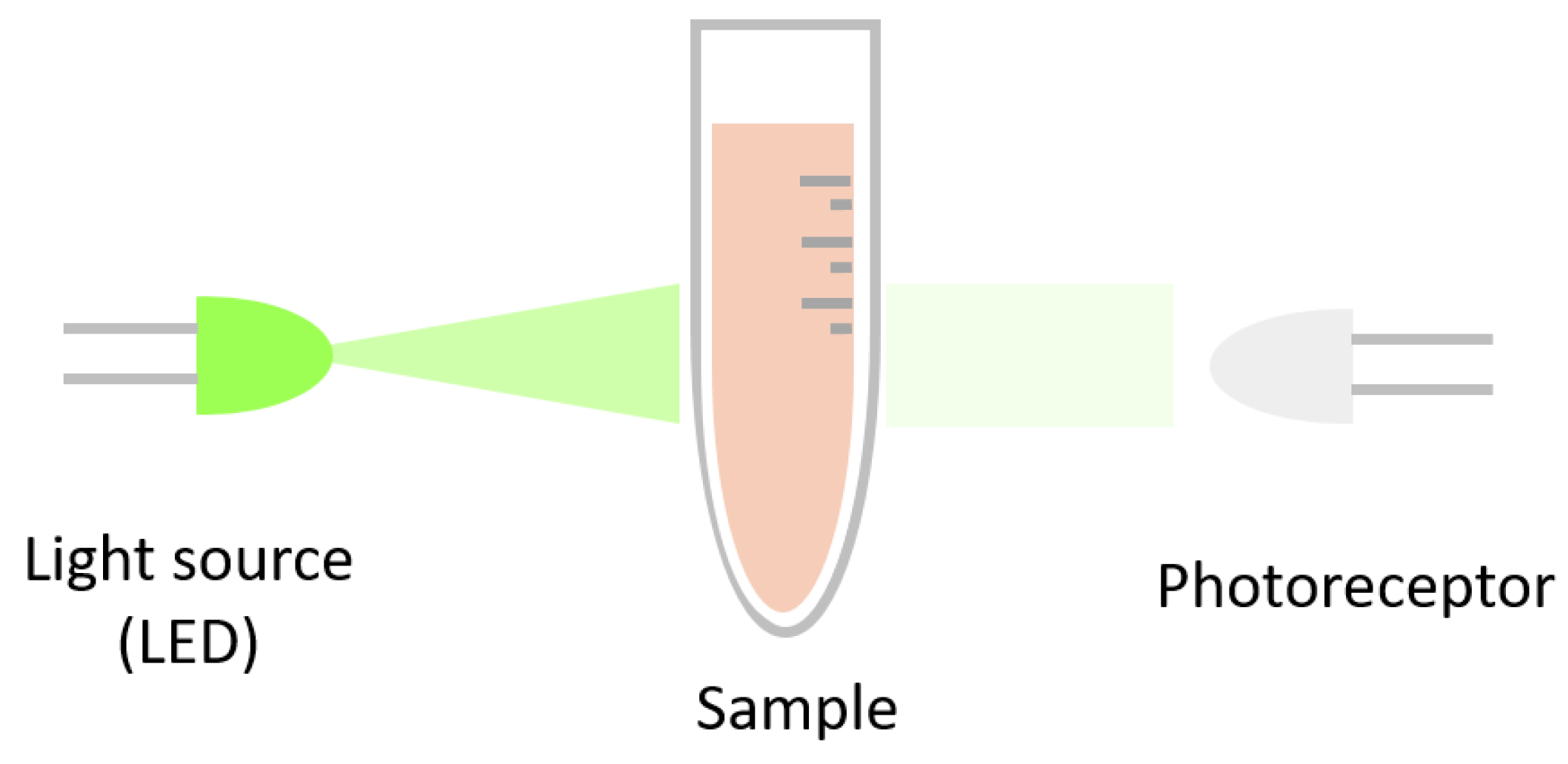
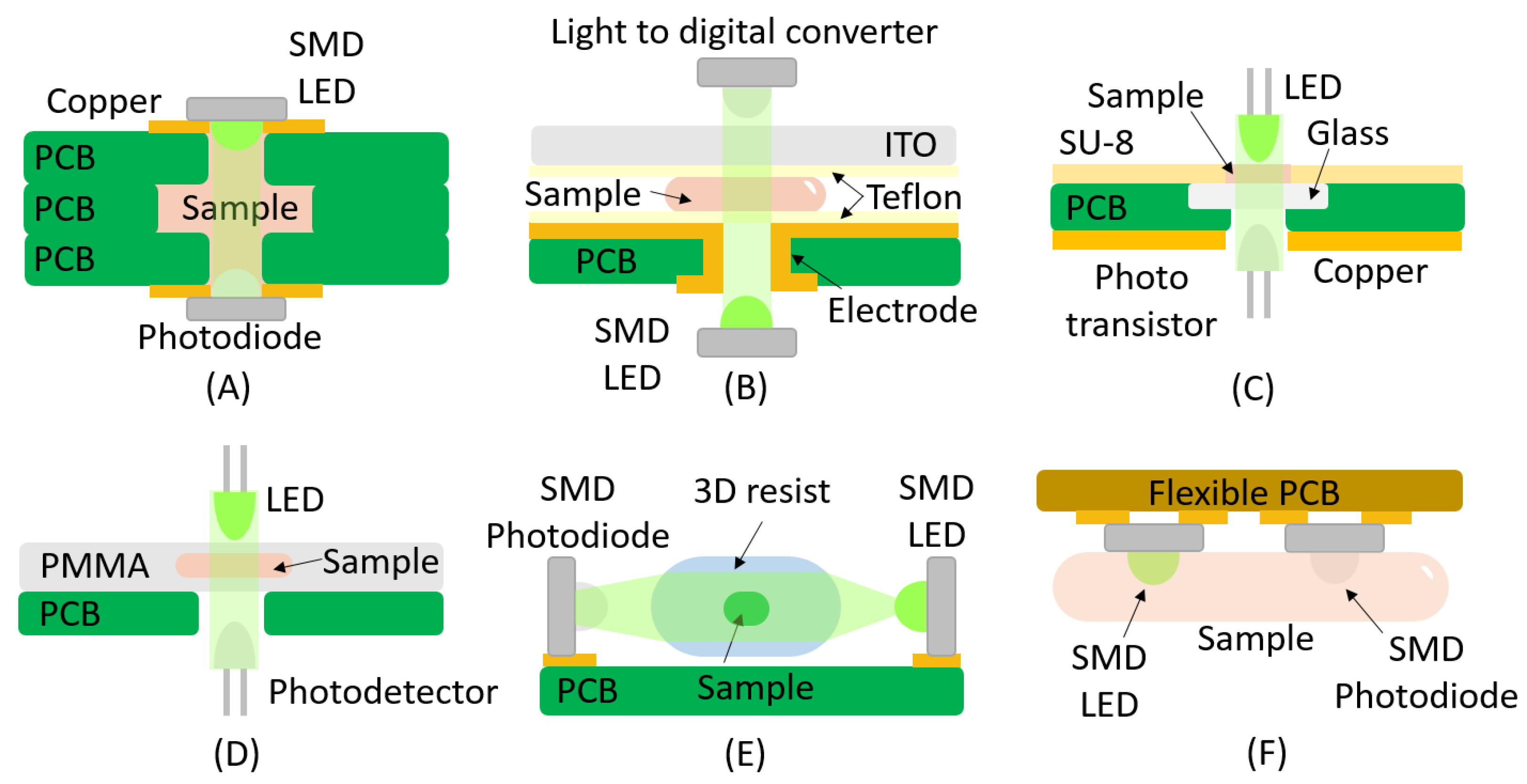
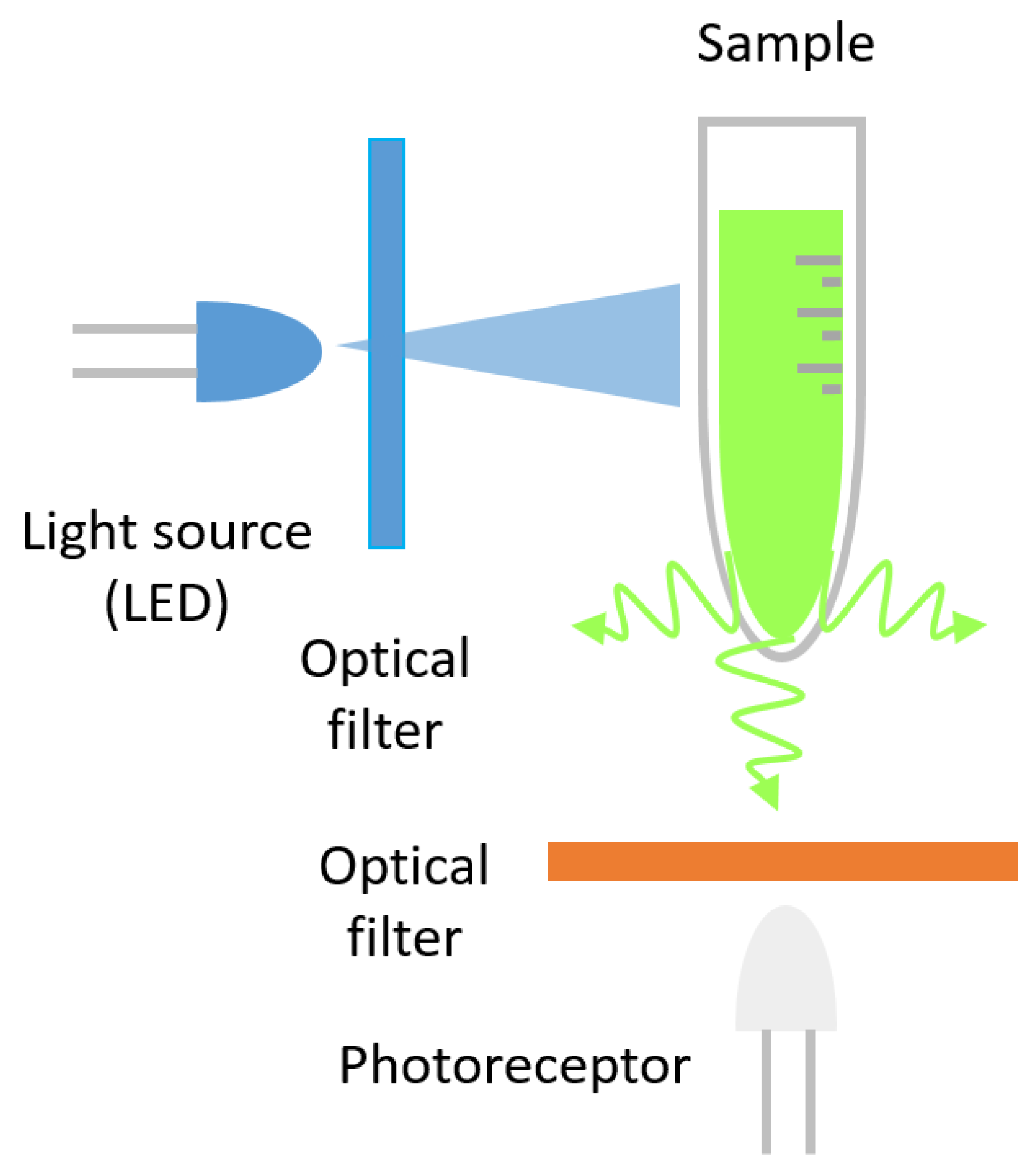
2. Absorbance
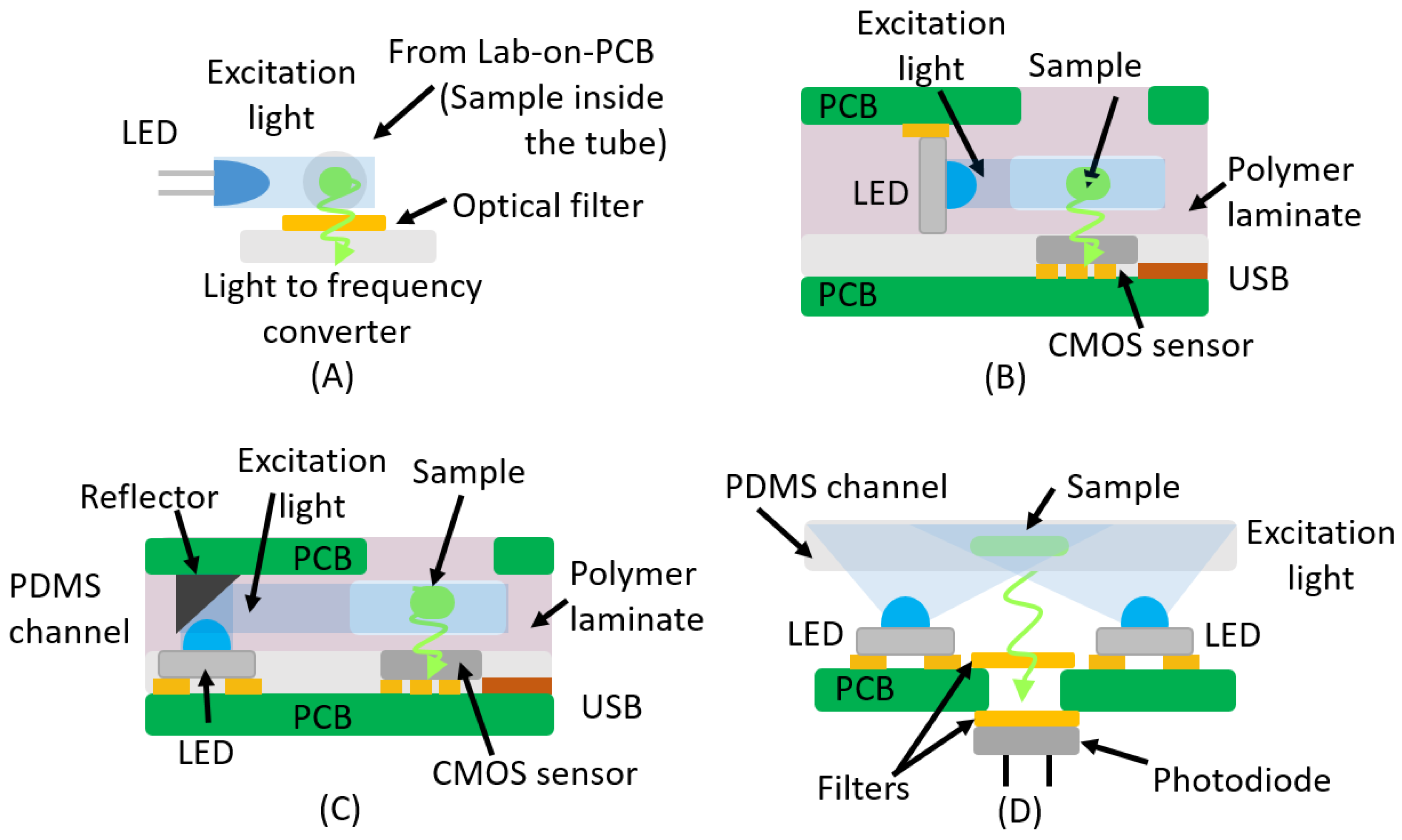
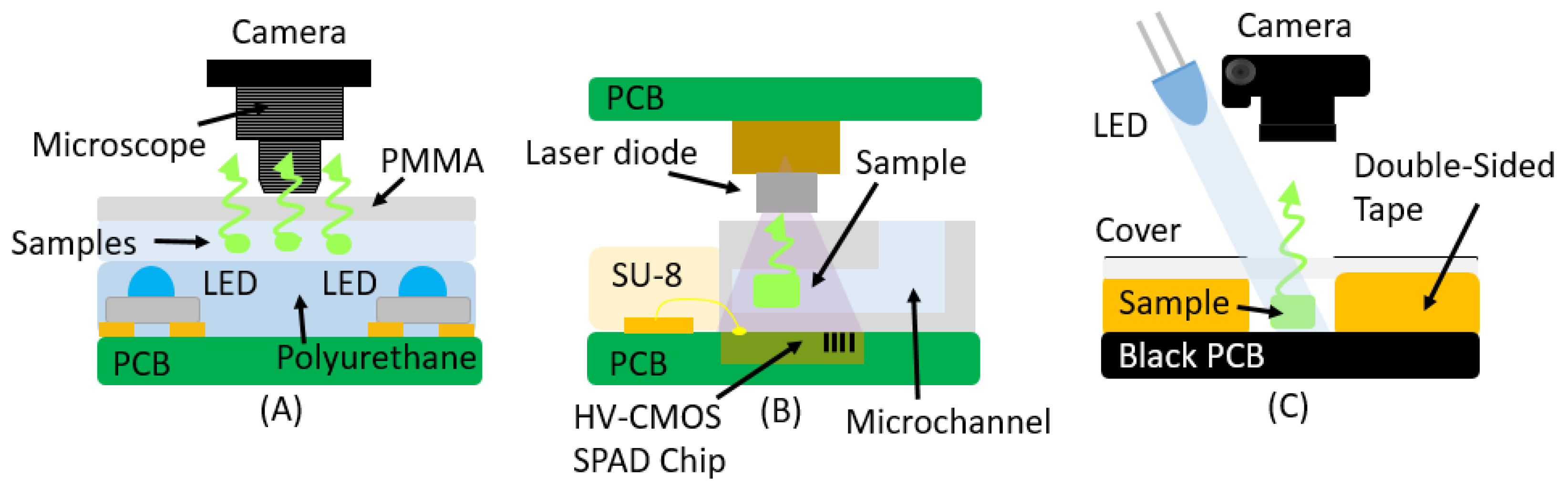
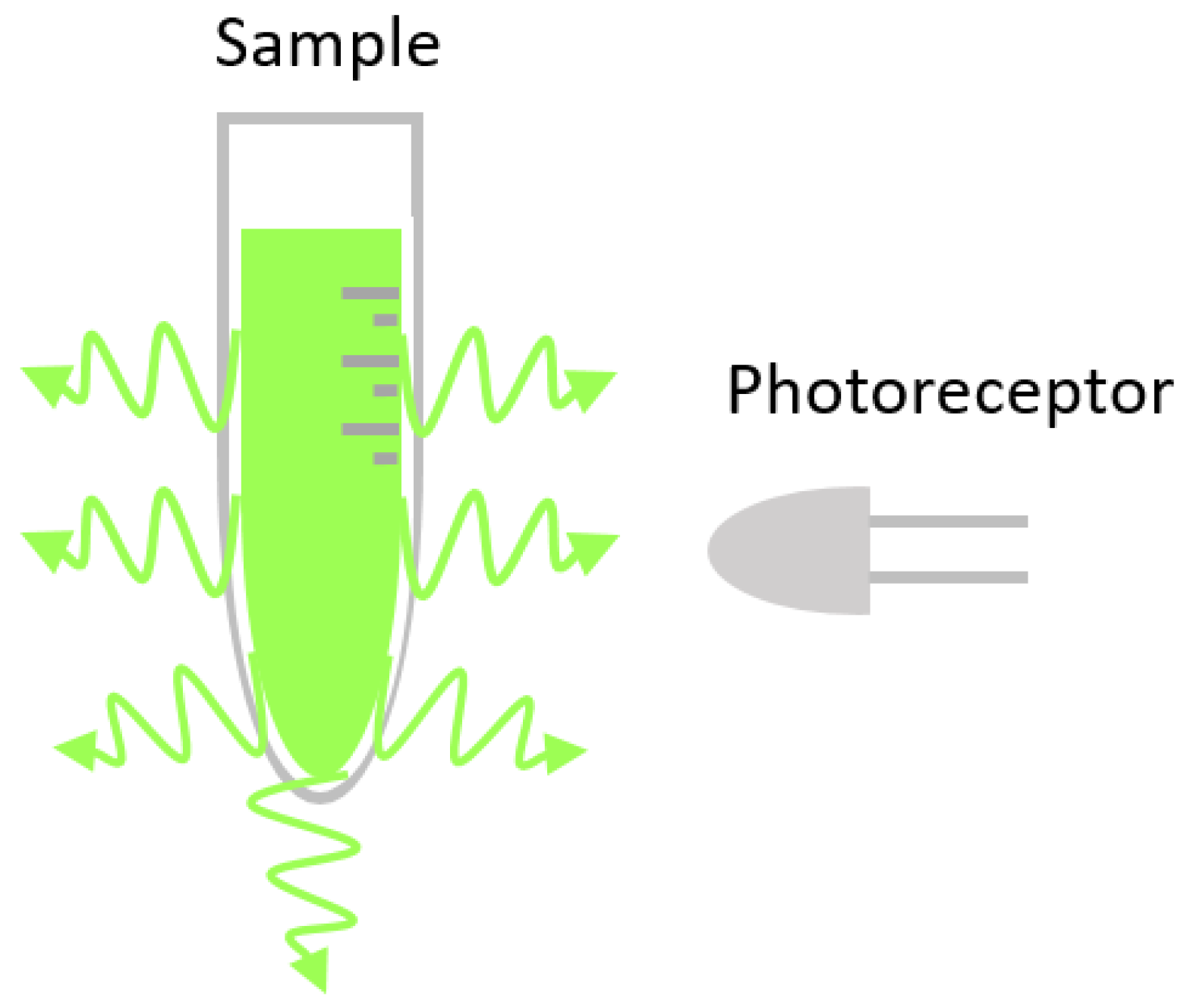
3. Fluorescence
4. Chemiluminescence
5. Other PCB-Based Methods
6. Discussion
7. Conclusions
Author Contributions
Funding
Data Availability Statement
Acknowledgments
Conflicts of Interest
References
- Perdigones, F.; Quero, J.M. Printed Circuit Boards: The Layers’ Functions for Electronic and Biomedical Engineering. Micromachines 2022, 13, 460. [Google Scholar] [CrossRef] [PubMed]
- Abgrall, P.; Gue, A. Lab-on-chip technologies: Making a microfluidic network and coupling it into a complete microsystem—A review. J. Micromech. Microeng. 2007, 17, R15. [Google Scholar] [CrossRef]
- Zhao, W.; Tian, S.; Huang, L.; Liu, K.; Dong, L. The review of Lab-on-PCB for biomedical application. Electrophoresis 2020, 41, 1433–1445. [Google Scholar] [CrossRef] [PubMed]
- Abbasi, R.; Hu, X.; Zhang, A.; Dummer, I.; Wachsmann-Hogiu, S. Optical Image Sensors for Smart Analytical Chemiluminescence Biosensors. Bioengineering 2024, 11, 912. [Google Scholar] [CrossRef]
- Van Ngoc, H.; Quyen, T.L.; Vinayaka, A.C.; Bang, D.D.; Wolff, A. Point-of-care system for rapid real-time detection of SARS-CoV-2 virus based on commercially available Arduino platforms. Front. Bioeng. Biotechnol. 2022, 10, 917573. [Google Scholar] [CrossRef]
- Kumar, A.; Nath, P.; Das, N.; Chatterjee, M.; Roy, P.; Satapathi, S. A 3D printing assisted microfluidic absorbance-based measurement system for biological assay. Meas. Sci. Technol. 2024, 35, 086007. [Google Scholar] [CrossRef]
- Zamboni, R.; Zaltron, A.; Izzo, E.; Bottaro, G.; Ferraro, D.; Sada, C. Opto-microfluidic system for absorbance measurements in lithium niobate device applied to ph measurements. Sensors 2020, 20, 5366. [Google Scholar] [CrossRef]
- Liao, Z.; Zhang, Y.; Li, Y.; Miao, Y.; Gao, S.; Lin, F.; Deng, Y.; Geng, L. Microfluidic chip coupled with optical biosensors for simultaneous detection of multiple analytes: A review. Biosens. Bioelectron. 2019, 126, 697–706. [Google Scholar] [CrossRef]
- Estevez, M.C.; Alvarez, M.; Lechuga, L.M. Integrated optical devices for lab-on-a-chip biosensing applications. Laser Photonics Rev. 2012, 6, 463–487. [Google Scholar] [CrossRef]
- Jokerst, N.M.; Luan, L.; Palit, S.; Royal, M.; Dhar, S.; Brooke, M.; Tyler, T., II. Progress in chip-scale photonic sensing. IEEE Trans. Biomed. Circuits Syst. 2009, 3, 202–211. [Google Scholar] [CrossRef]
- Gupta, S.; Ramesh, K.; Ahmed, S.; Kakkar, V. Lab-on-chip technology: A review on design trends and future scope in biomedical applications. Int. J. Bio-Sci. Bio-Technol 2016, 8, 311–322. [Google Scholar] [CrossRef]
- Blanco, F.J.; Agirregabiria, M.; Berganzo, J.; Mayora, K.; Elizalde, J.; Calle, A.; Domínguez, C.; Lechuga, L.M. Microfluidic-optical integrated CMOS compatible devices for label-free biochemical sensing. J. Micromech. Microeng. 2006, 16, 1006. [Google Scholar] [CrossRef]
- Senevirathna, B.; Lu, S.; Dandin, M.; Basile, J.; Smela, E.; Abshire, P. High resolution monitoring of chemotherapeutic agent potency in cancer cells using a CMOS capacitance biosensor. Biosens. Bioelectron. 2019, 142, 111501. [Google Scholar] [CrossRef] [PubMed]
- Jolly, P.; Rainbow, J.; Regoutz, A.; Estrela, P.; Moschou, D. A PNA-based Lab-on-PCB diagnostic platform for rapid and high sensitivity DNA quantification. Biosens. Bioelectron. 2019, 123, 244–250. [Google Scholar] [CrossRef]
- Cabello, M.; Mozo, M.; De la Cerda, B.; Aracil, C.; Diaz-Corrales, F.J.; Perdigones, F.; Valdes-Sanchez, L.; Relimpio, I.; Bhattacharya, S.S.; Quero, J.M. Electrostimulation in an autonomous culture lab-on-chip provides neuroprotection of a retinal explant from a retinitis pigmentosa mouse-model. Sens. Actuators B Chem. 2019, 288, 337–346. [Google Scholar] [CrossRef]
- Papamatthaiou, S.; Boxall-Clasby, J.; Douglas, E.J.; Jajesniak, P.; Peyret, H.; Mercer-Chalmers, J.; Kumar, V.K.; Lomonossoff, G.P.; Reboud, J.; Laabei, M.; et al. LoCKAmp: Lab-on-PCB technology for <3 min virus genetic detection. Lab Chip 2023, 23, 4400–4412. [Google Scholar]
- Anastasova, S.; Kassanos, P.; Yang, G.Z. Multi-parametric rigid and flexible, low-cost, disposable sensing platforms for biomedical applications. Biosens. Bioelectron. 2018, 102, 668–675. [Google Scholar] [CrossRef]
- Shamkhalichenar, H.; Bueche, C.J.; Choi, J.W. Printed circuit board (PCB) technology for electrochemical sensors and sensing platforms. Biosensors 2020, 10, 159. [Google Scholar] [CrossRef]
- Tseng, H.Y.; Adamik, V.; Parsons, J.; Lan, S.S.; Malfesi, S.; Lum, J.; Shannon, L.; Gray, B. Development of an electrochemical biosensor array for quantitative polymerase chain reaction utilizing three-metal printed circuit board technology. Sens. Actuators B Chem. 2014, 204, 459–466. [Google Scholar] [CrossRef]
- Nandakumar, V.; Bishop, D.; Alonas, E.; LaBelle, J.; Joshi, L.; Alford, T.L. A low-cost electrochemical biosensor for rapid bacterial detection. IEEE Sens. J. 2010, 11, 210–216. [Google Scholar] [CrossRef]
- Sánchez, J.A.; Henry, O.; Joda, H.; Solnestam, B.W.; Kvastad, L.; Johansson, E.; Akan, P.; Lundeberg, J.; Lladach, N.; Ramakrishnan, D.; et al. Multiplex PCB-based electrochemical detection of cancer biomarkers using MLPA-barcode approach. Biosens. Bioelectron. 2016, 82, 224–232. [Google Scholar] [CrossRef] [PubMed]
- Moschou, D.; Greathead, L.; Pantelidis, P.; Kelleher, P.; Morgan, H.; Prodromakis, T. Amperometric IFN-γ immunosensors with commercially fabricated PCB sensing electrodes. Biosens. Bioelectron. 2016, 86, 805–810. [Google Scholar] [CrossRef] [PubMed]
- Pu, Z.; Wang, R.; Wu, J.; Yu, H.; Xu, K.; Li, D. A flexible electrochemical glucose sensor with composite nanostructured surface of the working electrode. Sens. Actuators B Chem. 2016, 230, 801–809. [Google Scholar] [CrossRef]
- Damiati, S.; Søpstad, S.; Peacock, M.; Akhtar, A.S.; Pinto, I.; Soares, R.R.; Russom, A. Flex printed circuit board implemented graphene-based DNA sensor for detection of SARS-CoV-2. IEEE Sens. J. 2021, 21, 13060–13067. [Google Scholar] [CrossRef]
- Dutta, G.; Regoutz, A.; Moschou, D. Commercially fabricated printed circuit board sensing electrodes for biomarker electrochemical detection: The importance of electrode surface characteristics in sensor performance. Proceedings 2018, 2, 741. [Google Scholar] [CrossRef]
- Swinehart, D.F. The beer-lambert law. J. Chem. Educ. 1962, 39, 333. [Google Scholar] [CrossRef]
- Onorato, P.; Gratton, L.M.; Polesello, M.; Salmoiraghi, A.; Oss, S. The Beer Lambert law measurement made easy. Phys. Educ. 2018, 53, 035033. [Google Scholar] [CrossRef]
- Mayerhöfer, T.G.; Popp, J. Beer’s Law–why absorbance depends (almost) linearly on concentration. ChemPhysChem 2019, 20, 511–515. [Google Scholar] [CrossRef]
- Liang, Z.; Chiem, N.; Ocvirk, G.; Tang, T.; Fluri, K.; Harrison, D.J. Microfabrication of a planar absorbance and fluorescence cell for integrated capillary electrophoresis devices. Anal. Chem. 1996, 68, 1040–1046. [Google Scholar] [CrossRef]
- Gassmann, S.; Schleifer, T.; Schuette, H. Deployable Lab-on-a-Chip Sensor for Colorimetric Measurements. Micromachines 2023, 14, 2102. [Google Scholar] [CrossRef]
- Thiha, A.; Ibrahim, F. A colorimetric enzyme-linked immunosorbent assay (ELISA) detection platform for a point-of-care dengue detection system on a lab-on-compact-disc. Sensors 2015, 15, 11431–11441. [Google Scholar] [CrossRef] [PubMed]
- Jung, D.G.; Jung, D.; Kong, S.H. A lab-on-a-chip-based non-invasive optical sensor for measuring glucose in saliva. Sensors 2017, 17, 2607. [Google Scholar] [CrossRef] [PubMed]
- Läritz, C.; Pagel, L. A microfluidic pH-regulation system based on printed circuit board technology. Sens. Actuators A Phys. 2000, 84, 230–235. [Google Scholar] [CrossRef]
- Gaßmann, S.; Ibendorf, I.; Pagel, L. Realization of a flow injection analysis in PCB technology. Sens. Actuators A Phys. 2007, 133, 231–235. [Google Scholar] [CrossRef]
- Gu, Z.; Wu, M.L.; Yan, B.Y.; Wang, H.F.; Kong, C. Integrated digital microfluidic platform for colorimetric sensing of nitrite. ACS Omega 2020, 5, 11196–11201. [Google Scholar] [CrossRef]
- Flores, G.; Perdigones, F.; Aracil, C.; Cabello, M.; Quero, J. Microfluidic platform with absorbance sensor for glucose detection. In Proceedings of the 2015 10th Spanish Conference on Electron Devices (CDE), Madrid, Spain, 11–13 February 2015; pp. 1–4. [Google Scholar]
- Perdigones, F.; Urbano-Gámez, J.D.; Cabello, M.; Esteban-Pérez, A.; Quintero, A.; Díaz-Campillejo, Á.; Quero, J.M. Lab-on-PCB With Pre-Stored Reagents at Low Temperature and Automatic Microfluidic Handling. J. Microelectromech. Syst. 2022, 31, 912–917. [Google Scholar] [CrossRef]
- Medrano Trujillo, J.I. Fabricación de Circuitos Microfluídicos sobre Sustrato PCB Empleando Impresora 3D SLA. Master’s Thesis, Universidad de Sevilla, Sevilla, Spain, 2024. [Google Scholar]
- Yuen, J.D.; Shriver-Lake, L.C.; Walper, S.A.; Zabetakis, D.; Breger, J.C.; Stenger, D.A. Microbial nanocellulose printed circuit boards for medical sensing. Sensors 2020, 20, 2047. [Google Scholar] [CrossRef]
- Young, M. Principles and technique of fluorescence microscopy. J. Cell Sci. 1961, 3, 419–449. [Google Scholar] [CrossRef]
- Lakowicz, J.R. Principles of Fluorescence Spectroscopy; Springer: Berlin/Heidelberg, Germany, 2006. [Google Scholar]
- Itagaki, H. Chapter 3—Fluorescence Spectroscopy. In Experimental Methods in Polymer Science; Tanaka, T., Ed.; Polymers, Interfaces and Biomaterials; Academic Press: Boston, MA, USA, 2000; pp. 155–260. [Google Scholar] [CrossRef]
- Walczak, R. Fluorescence detection by miniaturized instrumentation based on non-cooled CCD minicamera and dedicated for lab-on-a-chip applications. Biochip J. 2011, 5, 271–279. [Google Scholar] [CrossRef]
- Choi, G.; Prince, T.; Miao, J.; Cui, L.; Guan, W. Sample-to-answer palm-sized nucleic acid testing device towards low-cost malaria mass screening. Biosens. Bioelectron. 2018, 115, 83–90. [Google Scholar] [CrossRef]
- Gupta, P.; Mohan, A.; Mishra, A.; Nair, A.; Chowdhury, N.; Balekai, D.; Rai, K.; Prabhakar, A.; Saiyed, T. Multiplexed fluorescence and scatter detection with single cell resolution using on-chip fiber optics for droplet microfluidic applications. Microsyst. Nanoeng. 2024, 10, 35. [Google Scholar] [CrossRef] [PubMed]
- Pokrzywnicka, A.; Śniadek, P.; Walczak, R. Glass microprism matrix for fluorescence excitation in lab-on-a-chip platforms. J. Micromech. Microeng. 2021, 31, 125009. [Google Scholar] [CrossRef]
- Papamatthaiou, S.; Boxall-Clasby, J.; Kumar, V.K.; Di Lorenzo, M.; Reboud, J.; Cooper, J.M.; Estrela, P.; Kasprzyk-Hordern, B.; Moschou, D. Lab-on-pcb device for handheld, rapid, molecular sars-cov-2 diagnostic in wastewater. In Proceedings of the 26th International Conference on Miniaturized Systems for Chemistry and Life Sciences, MicroTAS 2022, Hangzhou, China, 23–27 October 2022; Chemical and Biological Microsystems Society: Cambridge, MA, USA, 2022; pp. 642–643. [Google Scholar]
- Babikian, S.; Li, G.; Bachman, M. Portable micro-fluidic-opto-electronic printed circuit board for isotachophoresis applications. In Proc. MicroTAS 2015; Curran Associates, Inc.: New York, NY, USA, 2015; pp. 1293–1295. [Google Scholar]
- Babikian, S.; Li, G.; Bachman, M. A digital signal processing-assisted microfluidic PCB for on-chip fluorescence detection. IEEE Trans. Compon. Packag. Manuf. Technol. 2017, 7, 846–854. [Google Scholar] [CrossRef]
- Babikian, S.; Soriano, B.; Li, G.; Bachman, M. Laminate materials for microfluidic PCBs. Int. Symp. Microelectron. 2012, 2012, 000162–000168. [Google Scholar] [CrossRef]
- Shin, Y.H.; Barnett, J.Z.; Song, E.; Gutierrez-Wing, M.T.; Rusch, K.A.; Choi, J.W. A portable fluorescent sensor for on-site detection of microalgae. Microelectron. Eng. 2015, 144, 6–11. [Google Scholar] [CrossRef]
- Wu, L.L.; Babikian, S.; Li, G.P.; Bachman, M. Microfluidic printed circuit boards. In Proceedings of the 2011 IEEE 61st Electronic Components and Technology Conference (ECTC), Lake Buena Vista, FL, USA, 31 May–3 June 2011; pp. 1576–1581. [Google Scholar]
- Canals, J.; Franch, N.; Alonso, O.; Vilà, A.; Diéguez, A. A point-of-care device for molecular diagnosis based on CMOS SPAD detectors with integrated microfluidics. Sensors 2019, 19, 445. [Google Scholar] [CrossRef]
- Hwang, J.S.; Kim, Y.S.; Song, H.J.; Kim, J.D.; Park, C.Y. Fluorescence detection test by black printed circuit board based microfluidic channel for polymerase chain reaction. Technol. Health Care 2016, 24, S139–S146. [Google Scholar] [CrossRef]
- Baeyens, W.; Schulman, S.; Calokerinos, A.; Zhao, Y.; Campana, A.M.G.; Nakashima, K.; De Keukeleire, D. Chemiluminescence-based detection: Principles and analytical applications in flowing streams and in immunoassays. J. Pharm. Biomed. Anal. 1998, 17, 941–953. [Google Scholar] [CrossRef]
- Miyawa, J.H.; Schulman, S.G. Luminescence Spectroscopy. In Handbook of Pharmaceutical Analysis; CRC Press: Boca Raton, FL, USA, 2001; pp. 446–485. [Google Scholar]
- Syed, A.J.; Anderson, J.C. Applications of bioluminescence in biotechnology and beyond. Chem. Soc. Rev. 2021, 50, 5668–5705. [Google Scholar] [CrossRef]
- Meng, C.; Knežević, S.; Du, F.; Guan, Y.; Kanoufi, F.; Sojic, N.; Xu, G. Recent advances in electrochemiluminescence imaging analysis. EScience 2022, 2, 591–605. [Google Scholar] [CrossRef]
- Chen, R.; McKeever, S.W. Theory of Thermoluminescence and Related Phenomena; World Scientific: Singapore, 1997. [Google Scholar]
- Canaparo, R.; Foglietta, F.; Giuntini, F.; Francovich, A.; Serpe, L. The bright side of sound: Perspectives on the biomedical application of sonoluminescence. Photochem. Photobiol. Sci. 2020, 19, 1114–1121. [Google Scholar] [CrossRef] [PubMed]
- Harvey, E.N. Sonoluminescence and sonic chemiluminescence. J. Am. Chem. Soc. 1939, 61, 2392–2398. [Google Scholar] [CrossRef]
- Gus’ kov, A.; Nekrasova, L.; Gornakova, A.; Shikunova, I. Crystallochemiluminescence of solutions. Crystallogr. Rep. 2014, 59, 758–761. [Google Scholar] [CrossRef]
- Klein, J.S.; Sun, C.; Pratx, G. Radioluminescence in biomedicine: Physics, applications, and models. Phys. Med. Biol. 2019, 64, 04TR01. [Google Scholar] [CrossRef]
- Dong, Z.; Du, F.; Hanif, S.; Tian, Y.; Xu, G. Development of chemiluminescent systems and devices for analytical applications. Chem. Commun. 2024, 60, 11837–11848. [Google Scholar] [CrossRef]
- Nascetti, A.; Mirasoli, M.; Marchegiani, E.; Zangheri, M.; Costantini, F.; Porchetta, A.; Iannascoli, L.; Lovecchio, N.; Caputo, D.; de Cesare, G.; et al. Integrated chemiluminescence-based lab-on-chip for detection of life markers in extraterrestrial environments. Biosens. Bioelectron. 2019, 123, 195–203. [Google Scholar] [CrossRef]
- Daniel, R.; Almog, R.; Ron, A.; Belkin, S.; Diamand, Y.S. Modeling and measurement of a whole-cell bioluminescent biosensor based on a single photon avalanche diode. Biosens. Bioelectron. 2008, 24, 882–887. [Google Scholar] [CrossRef]
- Roda, A.; Mirasoli, M.; Dolci, L.S.; Buragina, A.; Bonvicini, F.; Simoni, P.; Guardigli, M. Portable device based on chemiluminescence lensless imaging for personalized diagnostics through multiplex bioanalysis. Anal. Chem. 2011, 83, 3178–3185. [Google Scholar] [CrossRef]
- Abbasi, R.; Liu, J.; Suarasan, S.; Wachsmann-Hogiu, S. SE-ECL on CMOS: A miniaturized electrochemiluminescence biosensor. Lab Chip 2022, 22, 994–1005. [Google Scholar] [CrossRef]
- Jin, K.; Hu, C.; Hu, S.; Hu, C.; Li, J.; Ma, H. “One-to-three” droplet generation in digital microfluidics for parallel chemiluminescence immunoassays. Lab Chip 2021, 21, 2892–2900. [Google Scholar] [CrossRef]
- Zou, F.; Ruan, Q.; Lin, X.; Zhang, M.; Song, Y.; Zhou, L.; Zhu, Z.; Lin, S.; Wang, W.; Yang, C.J. Rapid, real-time chemiluminescent detection of DNA mutation based on digital microfluidics and pyrosequencing. Biosens. Bioelectron. 2019, 126, 551–557. [Google Scholar] [CrossRef] [PubMed]
- Evans, R.; Luan, L.; Jokerst, N.M.; Fair, R.B. Optical detection heterogeneously integrated with a coplanar digital microfluidic lab-on-a-chip platform. In Proceedings of the 2007 IEEE SENSORS, Atlanta, GA, USA, 28–31 October 2007; pp. 423–426. [Google Scholar]
- Luan, L.; Evans, R.D.; Jokerst, N.M.; Fair, R.B. Integrated optical sensor in a digital microfluidic platform. IEEE Sens. J. 2008, 8, 628–635. [Google Scholar] [CrossRef]
- Pittet, P.; Lu, G.N.; Galvan, J.M.; Ferrigno, R.; Blum, L.J.; Leca-Bouvier, B. PCB-based integration of electrochemiluminescence detection for microfluidic systems. Analyst 2007, 132, 409–411. [Google Scholar] [CrossRef] [PubMed]
- Pittet, P.; Lu, G.N.; Galvan, J.M.; Ferrigno, R.; Blum, L.J.; Leca-Bouvier, B.D. PCB technology-based electrochemiluminescence microfluidic device for low-cost portable analytical systems. IEEE Sens. J. 2008, 8, 565–571. [Google Scholar] [CrossRef]
- Delgado, S.M.T.; Kinahan, D.J.; Sandoval, F.S.; Julius, L.A.N.; Kilcawley, N.A.; Ducrée, J.; Mager, D. Fully automated chemiluminescence detection using an electrified-Lab-on-a-Disc (eLoaD) platform. Lab Chip 2016, 16, 4002–4011. [Google Scholar] [CrossRef]
- Bamiedakis, N.; Hutter, T.; Penty, R.V.; White, I.H.; Elliott, S.R. PCB-integrated optical waveguide sensors: An ammonia gas sensor. J. Light. Technol. 2013, 31, 1628–1635. [Google Scholar] [CrossRef]
- Chandrappan, J.; Kuruveettil, H.; Wei, T.C.; Liang, C.T.W.; Ramana, P.V.; Suzuki, K.; Shioda, T.; Lau, J. Development of Performance Characterization Methods for Optoelectronic Circuit Boards. In Proceedings of the 2008 10th Electronics Packaging Technology Conference, Singapore, 9–12 December 2008; pp. 1108–1113. [Google Scholar]
- Chang, C.; Chang, C.; Lau, J.H.; Chang, A.; Tang, T.; Chiang, S.; Lee, M.; Tseng, T.; Wei, T.C.; Shiah, L.L.; et al. Fabrication of fully embedded board-level optical interconnects and optoelectronic printed circuit boards. In Proceedings of the 2009 11th Electronics Packaging Technology Conference, Singapore, 9–11 December 2009; pp. 973–976. [Google Scholar]
- Hartwig, H.; Sergeeva, E.; Thomas, N.; Hohlfeld, D. Precision laser direct writing of polymer optical waveguides and optofluidic systems. In DGaO Proceedings; Deutsche Gesellschaft für angewandte Optik e.V.: Ilmenau, Germany, 2016. [Google Scholar]
- Immonen, M.P.; Karppinen, M.; Kivilahti, J.K. Investigation of environmental reliability of optical polymer waveguides embedded on printed circuit boards. Circuit World 2007, 33, 9–19. [Google Scholar] [CrossRef]
- Kopetz, S.; Cai, D.; Rabe, E.; Neyer, A. PDMS-based optical waveguide layer for integration in electrical–optical circuit boards. AEU-Int. J. Electron. Commun. 2007, 61, 163–167. [Google Scholar] [CrossRef]
- Sergeeva, E.; Hartwig, H.; Hohlfeld, D. Optofluidic cuvettes with integrated polymer waveguides for fluid analysis on printed circuit boards. In Proceedings of the MikroSystemTechnik 2017 Congress, Munich, Germany, 23–25 October 2017; pp. 1–4. [Google Scholar]
- Wang, D.S.; Fan, S.K. Microfluidic surface plasmon resonance sensors: From principles to point-of-care applications. Sensors 2016, 16, 1175. [Google Scholar] [CrossRef]
- Liedberg, B.; Nylander, C.; Lundström, I. Biosensing with surface plasmon resonance—How it all started. Biosens. Bioelectron. 1995, 10, i–ix. [Google Scholar] [CrossRef]
- Suzuki, H.; Sugimoto, M.; Matsui, Y.; Kondoh, J. Effects of gold film thickness on spectrum profile and sensitivity of a multimode-optical-fiber SPR sensor. Sens. Actuators B Chem. 2008, 132, 26–33. [Google Scholar] [CrossRef]
- Lopez, G.A.; Estevez, M.C.; Soler, M.; Lechuga, L.M. Recent advances in nanoplasmonic biosensors: Applications and lab-on-a-chip integration. Nanophotonics 2017, 6, 123–136. [Google Scholar] [CrossRef]
- Hiep, H.M.; Nakayama, T.; Saito, M.; Yamamura, S.; Takamura, Y.; Tamiya, E. A microfluidic chip based on localized surface plasmon resonance for real-time monitoring of antigen–antibody reactions. Jpn. J. Appl. Phys. 2008, 47, 1337. [Google Scholar] [CrossRef]
- Mayer, K.M.; Hafner, J.H. Localized surface plasmon resonance sensors. Chem. Rev. 2011, 111, 3828–3857. [Google Scholar] [CrossRef]
- Kazuma, E.; Tatsuma, T. Localized surface plasmon resonance sensors based on wavelength-tunable spectral dips. Nanoscale 2014, 6, 2397–2405. [Google Scholar] [CrossRef]
- Huang, C.; Bonroy, K.; Reekmans, G.; Laureyn, W.; Verhaegen, K.; De Vlaminck, I.; Lagae, L.; Borghs, G. Localized surface plasmon resonance biosensor integrated with microfluidic chip. Biomed. Microdevices 2009, 11, 893–901. [Google Scholar] [CrossRef]
- Ouellet, E.; Lausted, C.; Lin, T.; Yang, C.W.T.; Hood, L.; Lagally, E.T. Parallel microfluidic surface plasmon resonance imaging arrays. Lab Chip 2010, 10, 581–588. [Google Scholar] [CrossRef]
- Obreja, P.; Cristea, D.; Kusko, M.; Dinescu, A. Polymer-based chips for surface plasmon resonance sensors. J. Opt. A Pure Appl. Opt. 2008, 10, 064010. [Google Scholar] [CrossRef]
- Teran, D.H.S.; Piñón, M.V.; Luque, A.; López, R.R.; Camacho-León, S. On the calibration of an optical, high-speed, multiphase microfluidic sensor with droplet counting applications in Lab-on-PCB devices. IEEE Sens. J. 2022, 22, 9509–9520. [Google Scholar] [CrossRef]
- Urbano-Gámez, J.D.; Perdigones, F.; Quero, J.M. Semi-Automatic Lab-on-PCB System for Agarose Gel Preparation and Electrophoresis for Biomedical Applications. Micromachines 2021, 12, 1071. [Google Scholar] [CrossRef]
- Do, M.T.; Nguyen, T.T.N.; Li, Q.; Benisty, H.; Ledoux-Rak, I.; Lai, N.D. Submicrometer 3D structures fabrication enabled by one-photon absorption direct laser writing. Opt. Express 2013, 21, 20964–20973. [Google Scholar] [CrossRef] [PubMed]
- Piruska, A.; Nikcevic, I.; Lee, S.H.; Ahn, C.; Heineman, W.R.; Limbach, P.A.; Seliskar, C.J. The autofluorescence of plastic materials and chips measured under laser irradiation. Lab Chip 2005, 5, 1348–1354. [Google Scholar] [CrossRef] [PubMed]
- Rondot, N.; Yan, S.; Mager, D.; Kulinsky, L. A low-cost printed circuit board-based centrifugal microfluidic platform for dielectrophoresis. Microsyst. Nanoeng. 2025, 11, 23. [Google Scholar] [CrossRef] [PubMed]


| Absorbance | ||||
|---|---|---|---|---|
| Excitation | Detection | Integrated | Characteristic | Reference |
| LED | Photodiode | Yes | SMD | [33,34] |
| LED | Photodiode | No | SMD | [35] |
| LED | Phototransistor | No | THT | [36] |
| LED | Photodetector | No | PCB Hole | [37] |
| LED | Photodiode | Yes | SMD Vertical/Lens | [38] |
| LED | Phototransistor | Yes | Flexible | [39] |
| Fluorescence | ||||
| Excitation | Detection | Integrated | Characteristic | Reference |
| LED | Light-to-frequency | No | THT LED | [16,47] |
| LED | CMOS Sensor | Yes | SMD/Reflector | [49,50] |
| LED | CMOS Sensor | Yes | SMD Vertical | [48] |
| LED | Photodiode | Yes | SMD/THT Perpendicular | [51] |
| LED | Inverted Microscope | Yes | Window | [52] |
| Laser diode | HV-CMOS SPAD | Yes | Embedded | [53] |
| LED | DSLR Camera | No | Black Solder Mask/White Silk | [54] |
| Chemiluminiscence | ||||
| Excitation | Detection | Integrated | Characteristic | Reference |
| N.A. | PMT | No | - | [69,70] |
| N.A. | InGaAs MSM detector | Yes | Teflon AF | [71,72] |
| N.A. | PMT | No | Optical Fiber | [73] |
| N.A. | PMT/CMOS BDJ | No | Optical Fiber | [74] |
| N.A. | SiPM | Yes | Modular | [75] |
| Other Methods | ||||
| Excitation | Detection | Integrated | Characteristic | Reference |
| Laser diode | AlGaAs/GaAs photodiodes | Yes | Polymer waveguides | [76] |
| LED | Photodiode | Yes | Polymer waveguides | [79] |
| Lamp | LDR | No | PCB Hole | [94] |
| LED | LDR | No | - | [93] |
Disclaimer/Publisher’s Note: The statements, opinions and data contained in all publications are solely those of the individual author(s) and contributor(s) and not of MDPI and/or the editor(s). MDPI and/or the editor(s) disclaim responsibility for any injury to people or property resulting from any ideas, methods, instructions or products referred to in the content. |
© 2025 by the authors. Licensee MDPI, Basel, Switzerland. This article is an open access article distributed under the terms and conditions of the Creative Commons Attribution (CC BY) license (https://creativecommons.org/licenses/by/4.0/).
Share and Cite
Perdigones, F.; Giménez-Gómez, P.; Muñoz-Berbel, X.; Aracil, C. Optical Detection Techniques for Biomedical Sensing: A Review of Printed Circuit Board (PCB)-Based Lab-on-Chip Systems. Micromachines 2025, 16, 564. https://doi.org/10.3390/mi16050564
Perdigones F, Giménez-Gómez P, Muñoz-Berbel X, Aracil C. Optical Detection Techniques for Biomedical Sensing: A Review of Printed Circuit Board (PCB)-Based Lab-on-Chip Systems. Micromachines. 2025; 16(5):564. https://doi.org/10.3390/mi16050564
Chicago/Turabian StylePerdigones, Francisco, Pablo Giménez-Gómez, Xavier Muñoz-Berbel, and Carmen Aracil. 2025. "Optical Detection Techniques for Biomedical Sensing: A Review of Printed Circuit Board (PCB)-Based Lab-on-Chip Systems" Micromachines 16, no. 5: 564. https://doi.org/10.3390/mi16050564
APA StylePerdigones, F., Giménez-Gómez, P., Muñoz-Berbel, X., & Aracil, C. (2025). Optical Detection Techniques for Biomedical Sensing: A Review of Printed Circuit Board (PCB)-Based Lab-on-Chip Systems. Micromachines, 16(5), 564. https://doi.org/10.3390/mi16050564