
Low Temperature Characteristics of Ge-on-Si Waveguide Photodetectors: A Combined Simulation and Experimental Study

 , , , and
Abstract
1. Introduction
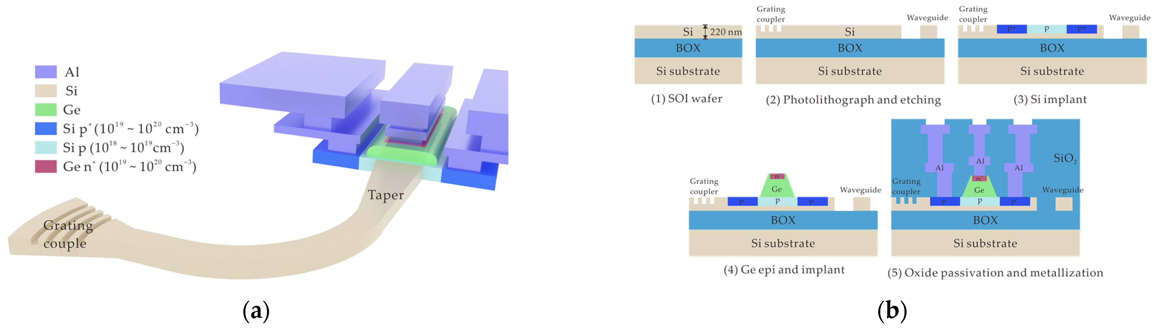
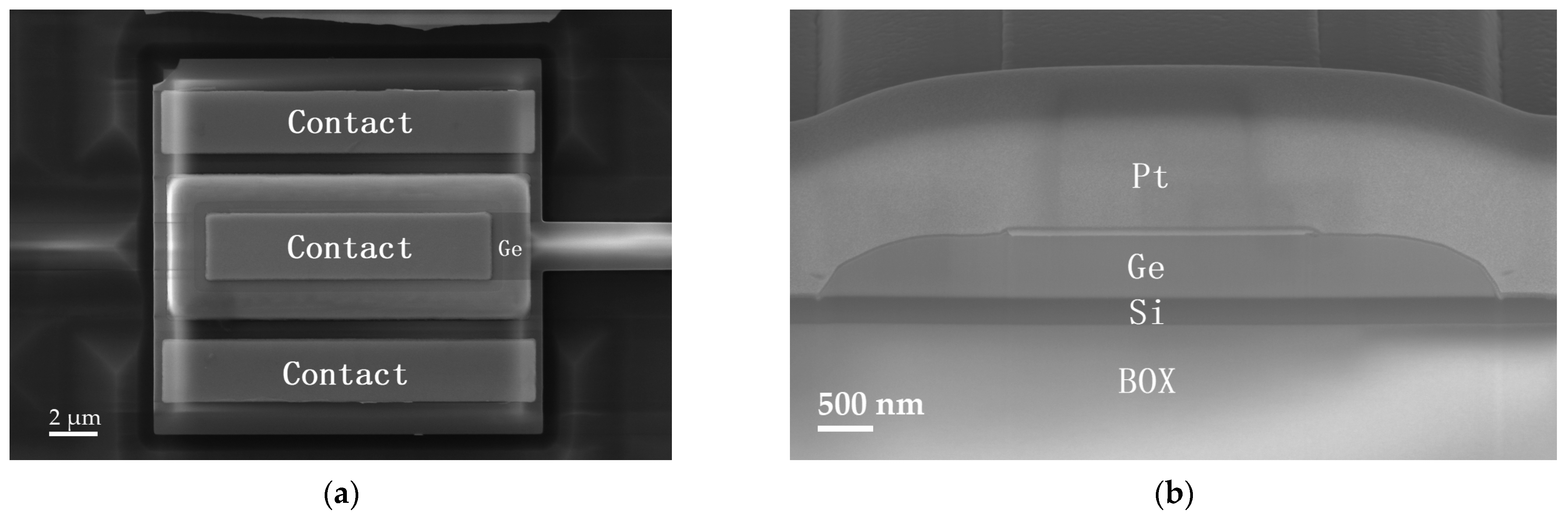
2. Device Structure
3. Results and Discussion
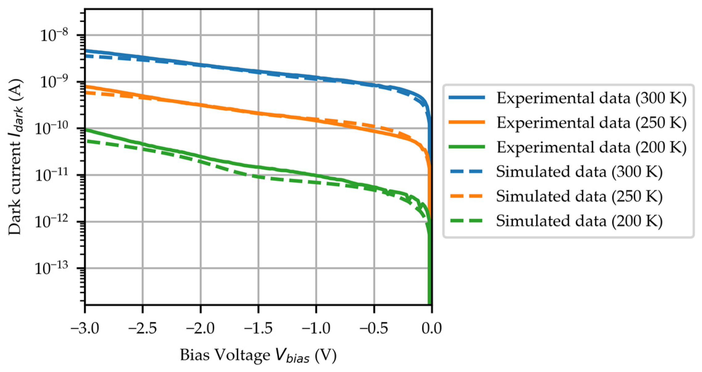
3.1. Dark Current Characteristics and the Simulation Model
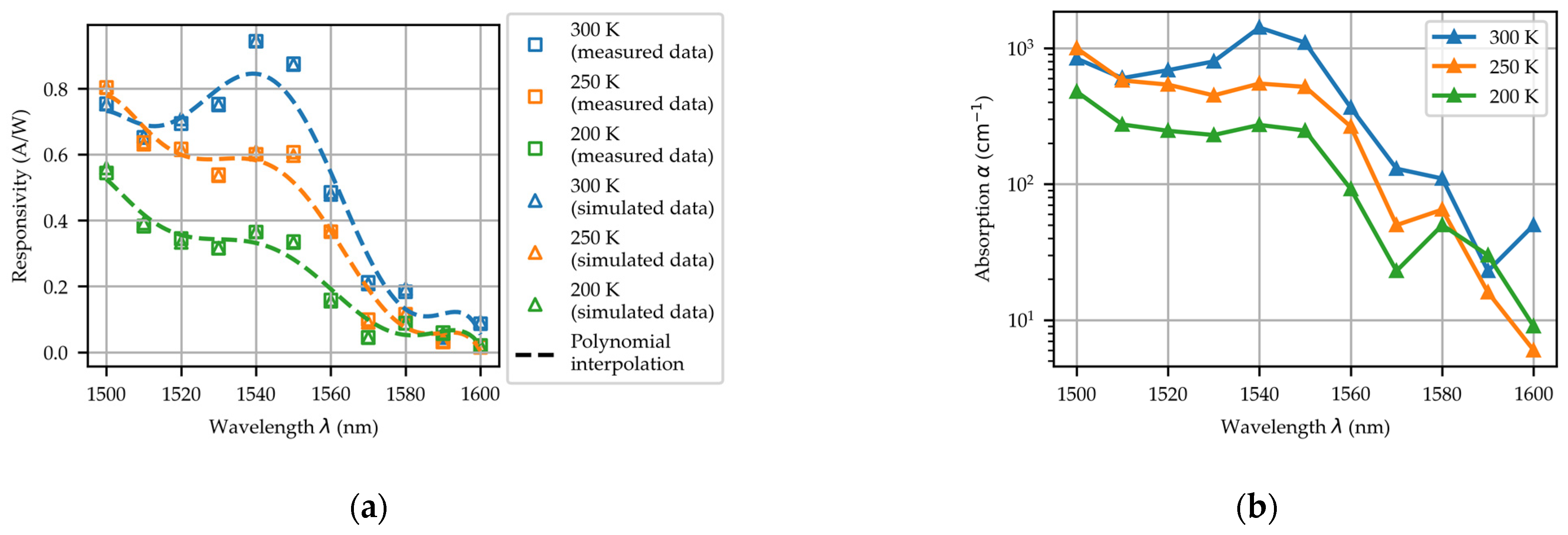
3.2. Photo-Response Characteristics and the Simulation Model
4. Conclusions
Author Contributions
Funding
Data Availability Statement
Conflicts of Interest
References
- Ben Yoo, S.J.; Proietti, R.; Grani, P. Photonics in Data Centers. In Optical Switching in Next Generation Data Centers; Testa, F., Pavesi, L., Eds.; Springer: Cham, Switzerland, 2018; pp. 3–21. [Google Scholar]
- Chaintoutis, C.; Shariati, B.; Bogris, A.; Dijk, P.V.; Roeloffzen, C.G.H.; Bourderionnet, J.; Tomkos, I.; Syvridis, D. Free Space Intra-Datacenter Interconnects Based on 2d Optical Beam Steering Enabled by Photonic Integrated Circuits. Photonics 2018, 5, 21. [Google Scholar] [CrossRef]
- Sun, C.; Wade, M.T.; Lee, Y.; Orcutt, J.S.; Alloatti, L.; Georgas, M.S.; Waterman, A.S.; Shainline, J.M.; Avizienis, R.R.; Lin, S.; et al. Single-Chip Microprocessor That Communicates Directly Using Light. Nature 2015, 528, 534–538. [Google Scholar] [CrossRef] [PubMed]
- Ning, S.; Zhu, H.; Feng, C.; Gu, J.; Jiang, Z.; Ying, Z.; Midkiff, J.; Jain, S.; Hlaing, M.H.; Pan, D.Z.; et al. Photonic-Electronic Integrated Circuits for High-Performance Computing and Ai Accelerators. J. Light. Technol. 2024, 42, 7834–7859. [Google Scholar] [CrossRef]
- Lim, A.E.J.; Song, J.; Fang, Q.; Li, C.; Tu, X.; Duan, N.; Chen, K.K.; Tern, R.P.C.; Liow, T.Y. Review of Silicon Photonics Foundry Efforts. IEEE J. Sel. Top. Quantum Electron. 2014, 20, 405–416. [Google Scholar] [CrossRef]
- Siew, S.Y.; Li, B.; Gao, F.; Zheng, H.Y.; Zhang, W.; Guo, P.; Xie, S.W.; Song, A.; Dong, B.; Luo, L.W.; et al. Review of Silicon Photonics Technology and Platform Development. J. Light. Technol. 2021, 39, 4374–4389. [Google Scholar] [CrossRef]
- Saha, N.; Brunetti, G.; di Toma, A.; Armenise, M.N.; Ciminelli, C. Silicon Photonic Filters: A Pathway from Basics to Applications. Adv. Photonics Res. 2024, 5, 2300343. [Google Scholar] [CrossRef]
- Zhou, Z. Recent Development in Photonic Integration. In Proceedings of the 2nd International Academic Conference on Optics and Photonics (IACOP 2024), Haikou, China, 19 February 2025. [Google Scholar]
- Amanti, F.; Andrini, G.; Armani, F.; Barbato, F.; Bellani, V.; Bonaiuto, V.; Cammarata, S.; Campostrini, M.; Dao, T.H.; De Matteis, F.; et al. Integrated Photonic Passive Building Blocks on Silicon-on-Insulator Platform. Photonics 2024, 11, 494. [Google Scholar] [CrossRef]
- Vitali, V.; Domínguez Bucio, T.; Lacava, C.; Marchetti, R.; Mastronardi, L.; Rutirawut, T.; Churchill, G.; Faneca, J.; Gates, J.C.; Gardes, F.; et al. High-Efficiency Reflector-Less Dual-Level Silicon Photonic Grating Coupler. Photon. Res. 2023, 11, 1275–1283. [Google Scholar] [CrossRef]
- Yi, Q.; Cheng, G.; Yan, Z.; Li, Q.; Xu, F.; Zou, Y.; Li, T.; Sun, Y.; Zou, Y.; Yu, Y.; et al. Silicon Mmi-Based Power Splitter for Multi-Band Operation at the 1.55 and 2 µm Wave Bands. Opt. Lett. 2023, 48, 1335–1338. [Google Scholar] [CrossRef]
- Bogaerts, W.; De Heyn, P.; Van Vaerenbergh, T.; De Vos, K.; Kumar Selvaraja, S.; Claes, T.; Dumon, P.; Bienstman, P.; Van Thourhout, D.; Baets, R. Silicon Microring Resonators. Laser Photonics Rev. 2012, 6, 47–73. [Google Scholar] [CrossRef]
- Lu, Z.; Yun, H.; Wang, Y.; Chen, Z.; Zhang, F.; Jaeger, N.A.F.; Chrostowski, L. Broadband Silicon Photonic Directional Coupler Using Asymmetric-Waveguide Based Phase Control. Opt. Express 2015, 23, 3795–3808. [Google Scholar] [CrossRef] [PubMed]
- Michel, J.; Liu, J.; Kimerling, L.C. High-Performance Ge-on-Si Photodetectors. Nat. Photonics 2010, 4, 527–534. [Google Scholar] [CrossRef]
- Zhao, X.; Wang, G.; Lin, H.; Du, Y.; Luo, X.; Kong, Z.; Su, J.; Li, J.; Xiong, W.; Miao, Y.; et al. High Performance P-I-N Photodetectors on Ge-on-Insulator Platform. Nanomaterials 2021, 11, 1125. [Google Scholar] [CrossRef] [PubMed]
- Ishikawa, Y.; Wada, K.; Cannon, D.D.; Liu, J.; Luan, H.-C.; Kimerling, L.C. Strain-Induced Band Gap Shrinkage in Ge Grown on Si Substrate. Appl. Phys. Lett. 2003, 82, 2044–2046. [Google Scholar] [CrossRef]
- Shi, Y.; Li, X.; Zou, M.; Yu, Y.; Zhang, X. 103 Ghz Germanium-on-Silicon Photodiode Enabled by an Optimized U-Shaped Electrode. Photonics Res. 2024, 12, 1–6. [Google Scholar] [CrossRef]
- Yin, D.; He, T.; Han, Q.; Lü, Q.; Zhang, Y.; Yang, X. High-Responsivity 40 Gbit/S Ingaas/Inp Pin Photodetectors Integrated on Silicon-on-Insulator Waveguide Circuits. J. Semicond. 2016, 37, 114006. [Google Scholar] [CrossRef]
- Chen, W.-Y.; Shi, X.-L.; Zou, J.; Chen, Z.-G. Thermoelectric Coolers for on-Chip Thermal Management: Materials, Design, and Optimization. Mater. Sci. Eng. R Rep. 2022, 151, 100700. [Google Scholar] [CrossRef]
- Bhan, R.K.; Dhar, V. Recent Infrared Detector Technologies, Applications, Trends and Development of Hgcdte Based Cooled Infrared Focal Plane Arrays and Their Characterization. Opto-Electron. Rev. 2019, 27, 174–193. [Google Scholar] [CrossRef]
- Xu, J.; Shi, W.; Wen, X.; Lu, H.; Li, M. Temperature-Dependent Anomalous Dispersion of Polycrystalline Germanium Film near Absorption Threshold. Mater. Chem. Phys. 2020, 243, 122562. [Google Scholar] [CrossRef]
- Bansal, R.; Jheng, Y.T.; Lee, K.C.; Wen, S.; Berencén, Y.; Cheng, H.H.; Chang, G.E. Temperature-Dependent Characteristics of Gesn Waveguide P-I-N Photodetectors: Step Towards Cryogenic Silicon Photonics. IEEE J. Sel. Top. Quantum Electron. 2025, 31, 8200212. [Google Scholar] [CrossRef]
- Bradley, L.J.; Horsfall, A.B.; Dyson, A. Modeling the Key Material Properties of Germanium for Device Simulation in Cryogenic Environments. IEEE Trans. Electron Devices 2020, 67, 4099–4104. [Google Scholar] [CrossRef]
- Bradley, L. Modelling the Cryogenic Properties of Germanium for Emerging Liquid Hydrogen Power Applications. Ph.D. Thesis, Newcastle University, Tyne and Wear, UK, 2020. [Google Scholar]
- Boukhatem, M.H. Carriers Temperature Dependence of Energy Band Gap for Germanium. Silicon 2016, 8, 309–312. [Google Scholar] [CrossRef]
- Hellings, G.; Eneman, G.; Krom, R.; Jaeger, B.D.; Mitard, J.; Keersgieter, A.D.; Hoffmann, T.; Meuris, M.; Meyer, K.D. Electrical Tcad Simulations of a Germanium Pmosfet Technology. IEEE Trans. Electron Devices 2010, 57, 2539–2546. [Google Scholar] [CrossRef]
- Lautenschlager, P.; Allen, P.B.; Cardona, M. Temperature Dependence of Band Gaps in Si and Ge. Phys. Rev. B 1985, 31, 2163–2171. [Google Scholar] [CrossRef]
- Závěctová, M.; Voríček, V. Temperature Dependence of the Absorption Edge of Amorphous Germanium. Phys. Status Solidi B-Basic Res. 1971, 48, 113–118. [Google Scholar] [CrossRef]
- Hurkx, G.A.M.; Klaassen, D.B.M.; Knuvers, M.P.G. A New Recombination Model for Device Simulation Including Tunneling. IEEE Trans. Electron Devices 1992, 39, 331–338. [Google Scholar] [CrossRef]
- Grove, A.S. Physics and Technology of Semiconductor Devices; Wiley: Singapore, 1967. [Google Scholar]
- Chen, H.; Verheyen, P.; De Heyn, P.; Lepage, G.; De Coster, J.; Balakrishnan, S.; Absil, P.; Roelkens, G.; Van Campenhout, J. Dark Current Analysis in High-Speed Germanium P-I-N Waveguide Photodetectors. J. Appl. Phys. 2016, 119, 213105. [Google Scholar] [CrossRef]
- Arora, N.D.; Hauser, J.R.; Roulston, D.J. Electron and Hole Mobilities in Silicon as a Function of Concentration and Temperature. IEEE Trans. Electron Devices 1982, 29, 292–295. [Google Scholar] [CrossRef]
- Klaassen, D.B.M. A Unified Mobility Model for Device Simulation. In Proceedings of the International Technical Digest on Electron Devices, San Francisco, CA, USA, 9–12 December 1990. [Google Scholar]
- Caughey, D.M.; Thomas, R.E. Carrier Mobilities in Silicon Empirically Related to Doping and Field. Proc. IEEE 1967, 55, 2192–2193. [Google Scholar] [CrossRef]
- Li, H.H. Refractive Index of Silicon and Germanium and Its Wavelength and Temperature Derivatives. J. Phys. Chem. Ref. Data 1980, 9, 561–658. [Google Scholar] [CrossRef]
- Douglas, B.L.; Bradley, J.F. Temperature-Dependent Absolute Refractive Index Measurements of Synthetic Fused Silica. In Proceedings of the Optomechanical Technologies for Astronomy, Orlando, FL, USA, 6 July 2006. [Google Scholar]
- Frey, B.J.; Leviton, D.B.; Madison, T.J. Temperature-Dependent Refractive Index of Silicon and Germanium. In Proceedings of the Optomechanical Technologies for Astronomy, Orlando, FL, USA, 6 July 2006. [Google Scholar]


Disclaimer/Publisher’s Note: The statements, opinions and data contained in all publications are solely those of the individual author(s) and contributor(s) and not of MDPI and/or the editor(s). MDPI and/or the editor(s) disclaim responsibility for any injury to people or property resulting from any ideas, methods, instructions or products referred to in the content. |
© 2025 by the authors. Licensee MDPI, Basel, Switzerland. This article is an open access article distributed under the terms and conditions of the Creative Commons Attribution (CC BY) license (https://creativecommons.org/licenses/by/4.0/).
Share and Cite
Liu, J.; Li, Z.; Liu, X.; Yan, W.; Zhao, X.; Zheng, S.; Qiu, Y.; Zhong, Q.; Dong, Y.; Hu, T. Low Temperature Characteristics of Ge-on-Si Waveguide Photodetectors: A Combined Simulation and Experimental Study. Micromachines 2025, 16, 542. https://doi.org/10.3390/mi16050542
Liu J, Li Z, Liu X, Yan W, Zhao X, Zheng S, Qiu Y, Zhong Q, Dong Y, Hu T. Low Temperature Characteristics of Ge-on-Si Waveguide Photodetectors: A Combined Simulation and Experimental Study. Micromachines. 2025; 16(5):542. https://doi.org/10.3390/mi16050542
Chicago/Turabian StyleLiu, Jingchuan, Zhenyu Li, Xiaofei Liu, Wentao Yan, Xingyan Zhao, Shaonan Zheng, Yang Qiu, Qize Zhong, Yuan Dong, and Ting Hu. 2025. "Low Temperature Characteristics of Ge-on-Si Waveguide Photodetectors: A Combined Simulation and Experimental Study" Micromachines 16, no. 5: 542. https://doi.org/10.3390/mi16050542
APA StyleLiu, J., Li, Z., Liu, X., Yan, W., Zhao, X., Zheng, S., Qiu, Y., Zhong, Q., Dong, Y., & Hu, T. (2025). Low Temperature Characteristics of Ge-on-Si Waveguide Photodetectors: A Combined Simulation and Experimental Study. Micromachines, 16(5), 542. https://doi.org/10.3390/mi16050542