
Modeling of Multi-Cell HBT Device Based on Device Structure


Abstract
1. Introduction
2. Methods for Device Model Construction, Extraction, and Optimization
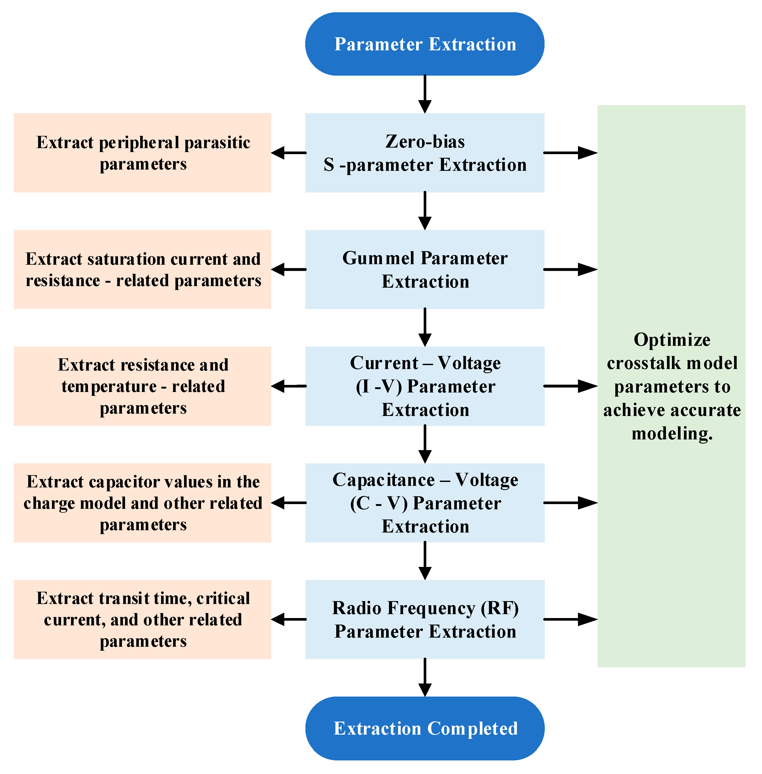
2.1. Model Parameter Extraction Process
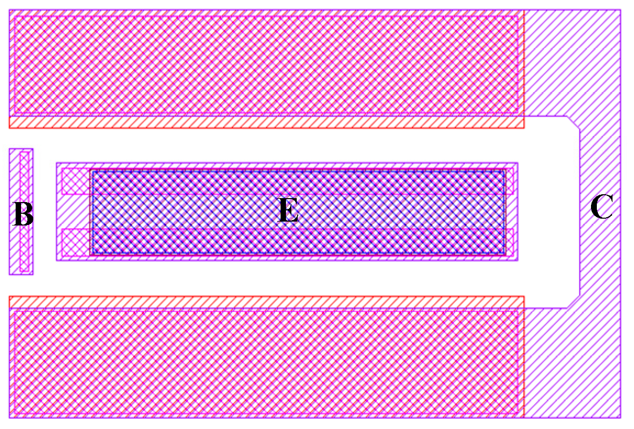
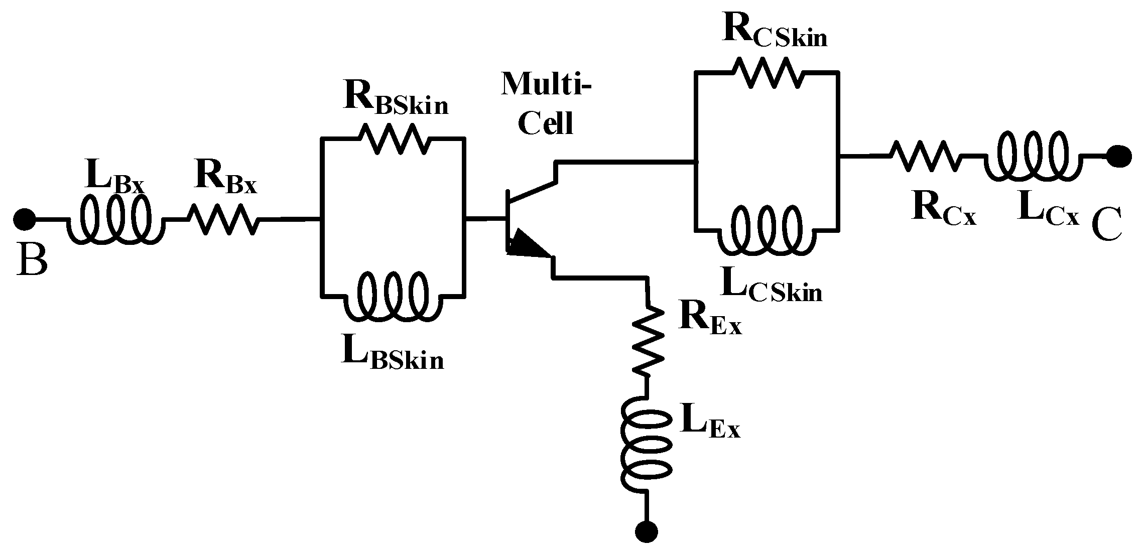
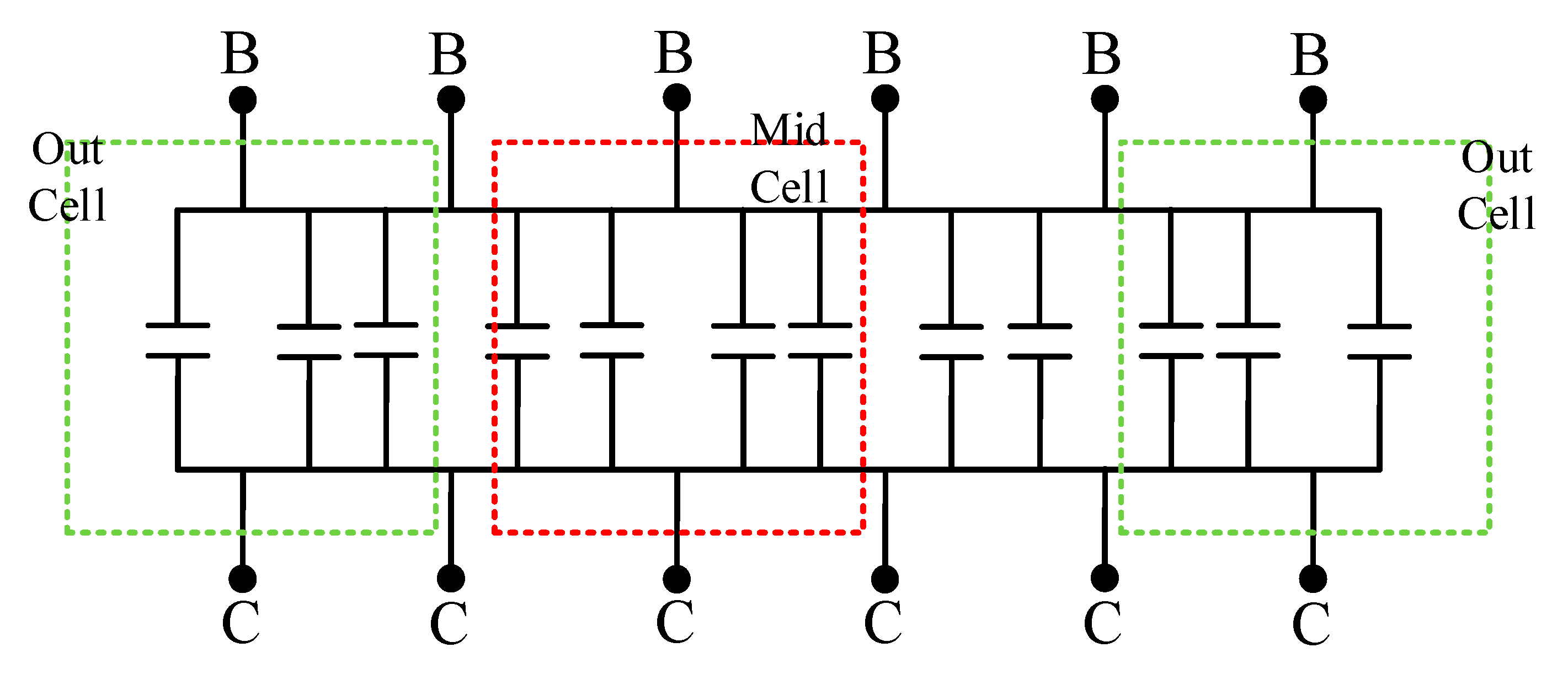
2.2. Peripheral Parasitic Extraction for a Multi-Cell Device
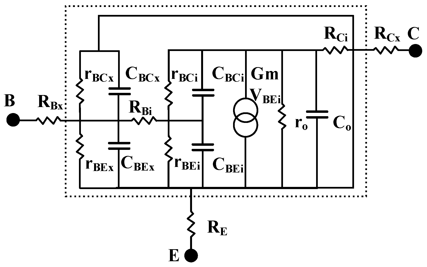
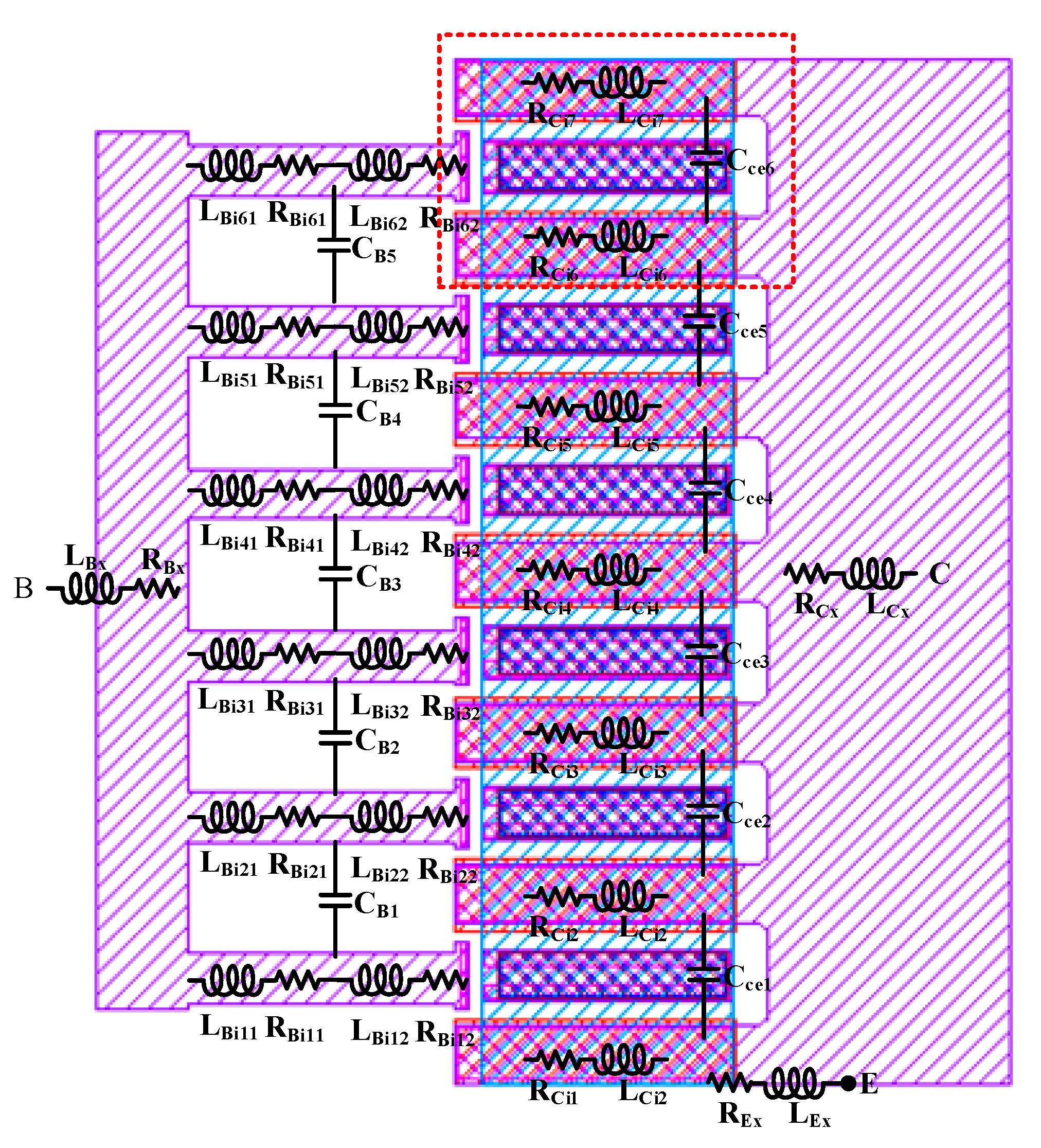
2.3. Model Parameter Extraction and Optimization for a Multi-Cell Device
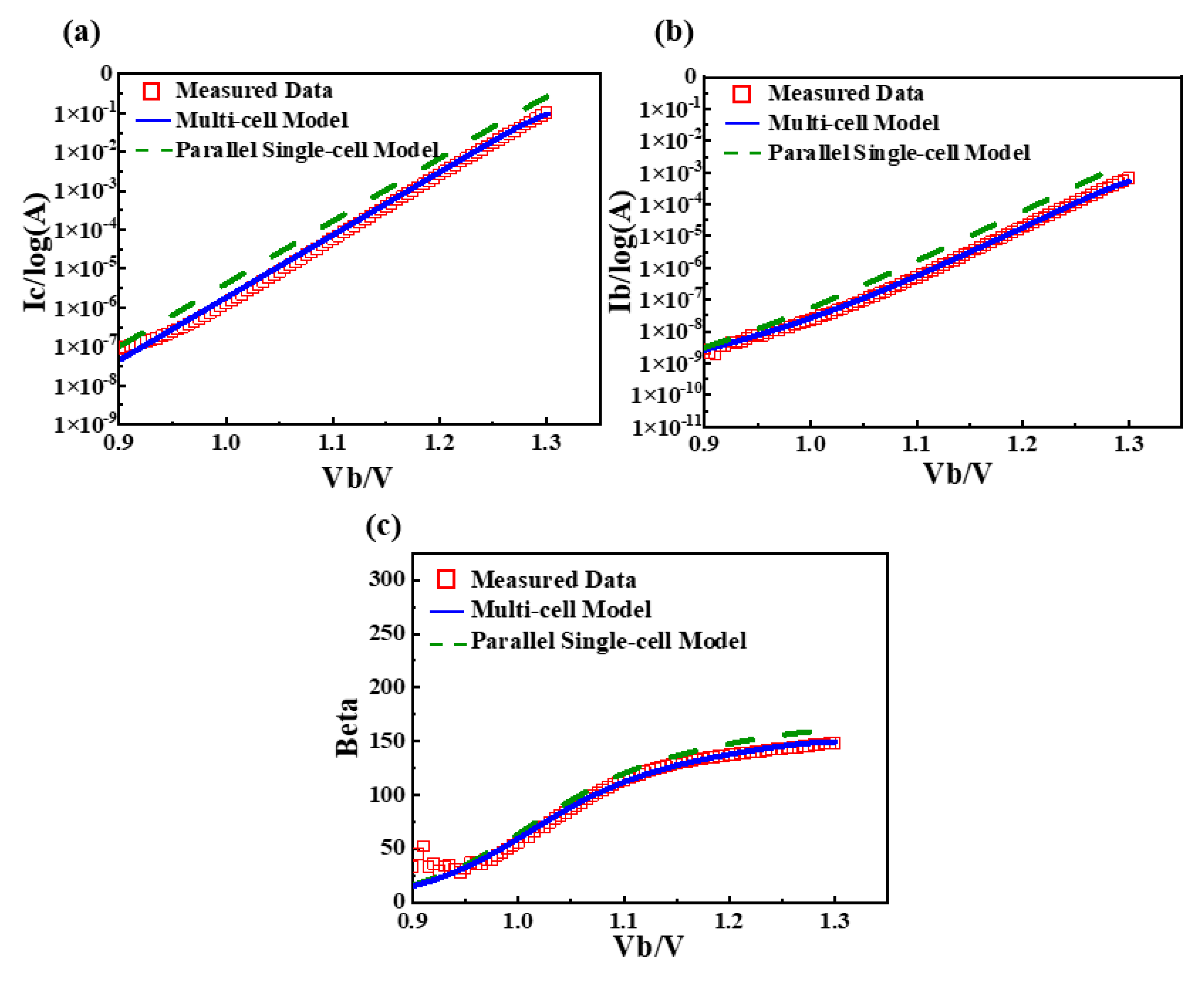
- Gummel parameter extraction
- 2.
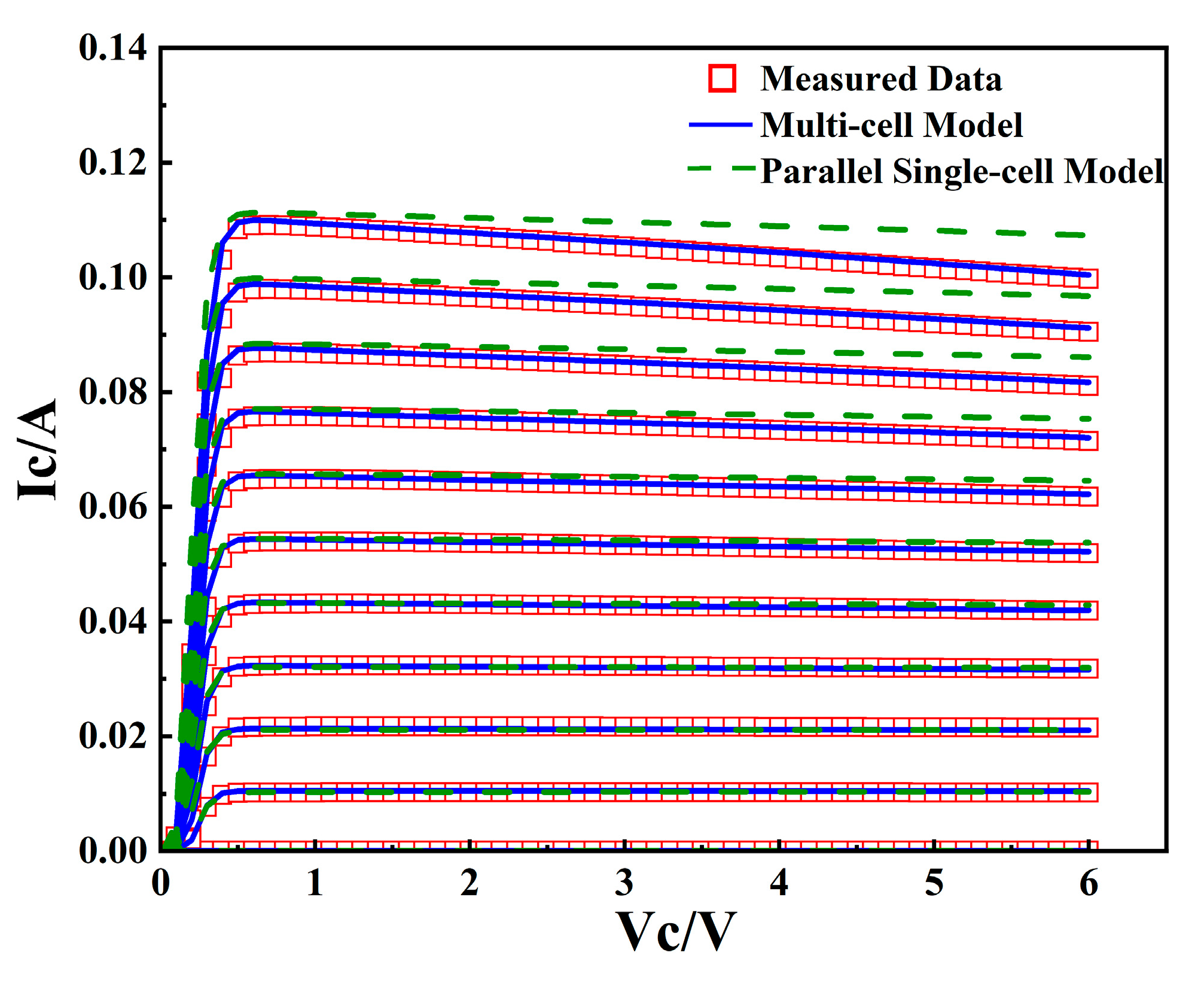
- Current-voltage parameter extraction
- 3.
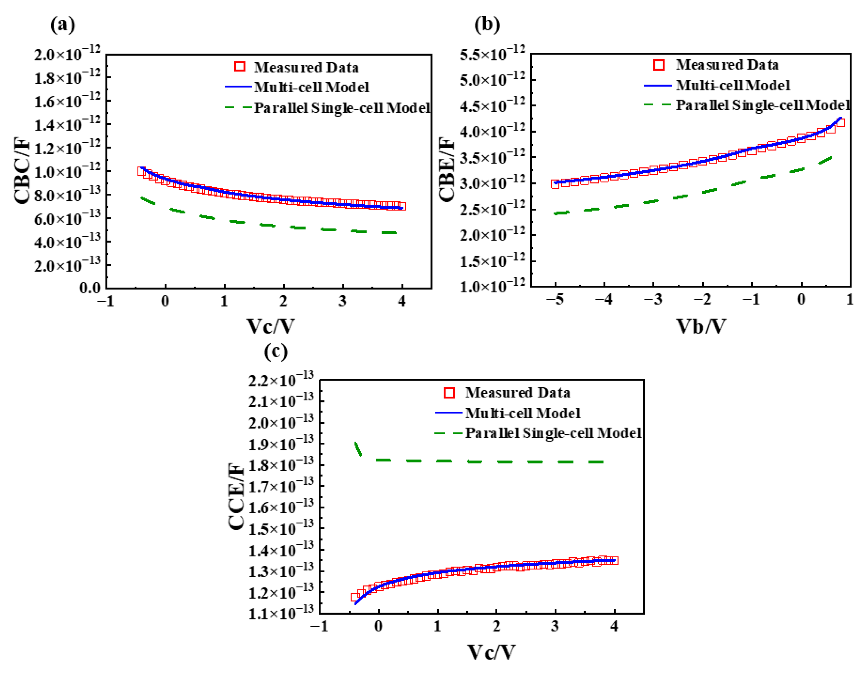
- Capacitance-voltage parameter extraction
- 4.
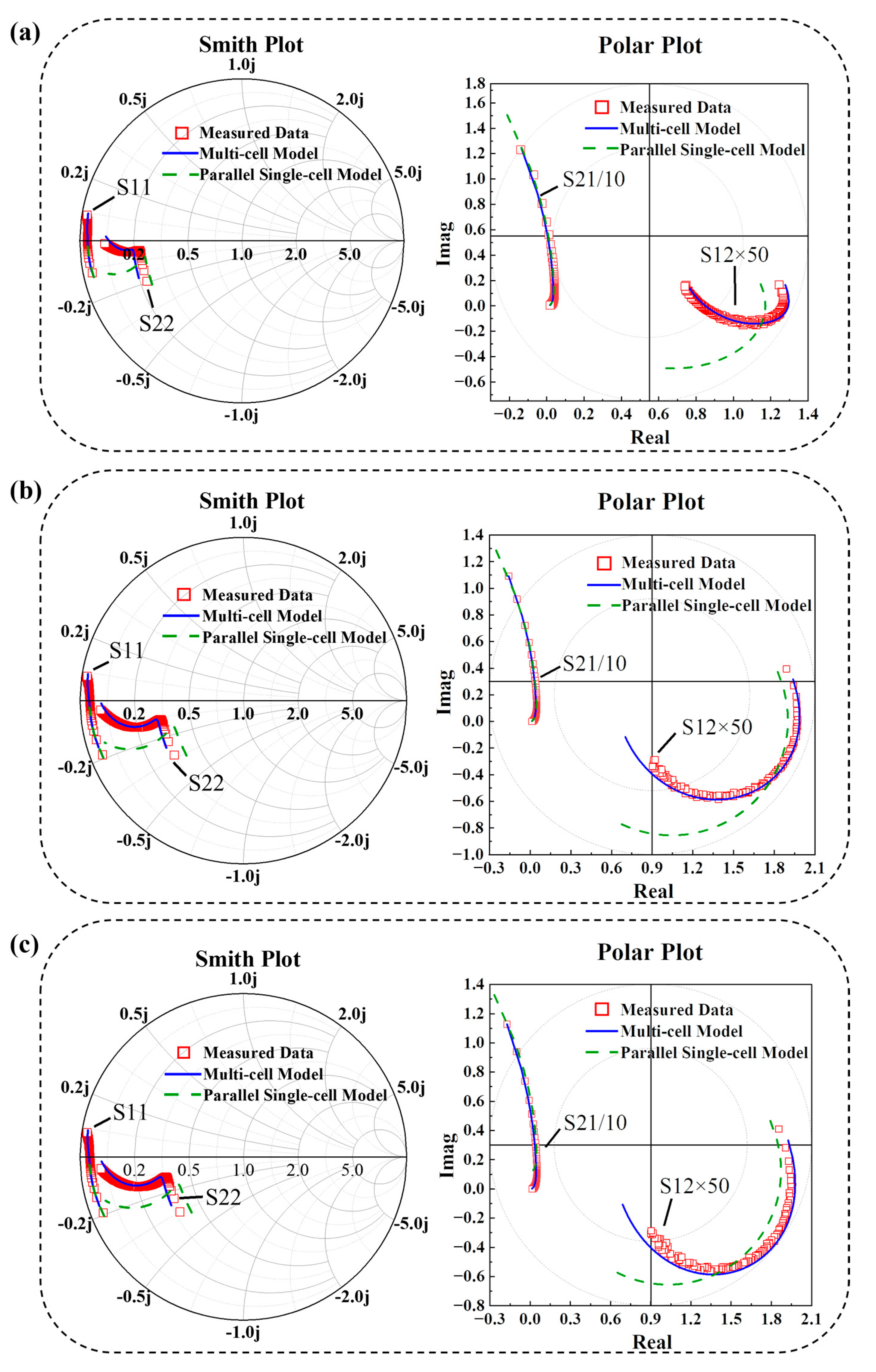
- RF parameter extraction
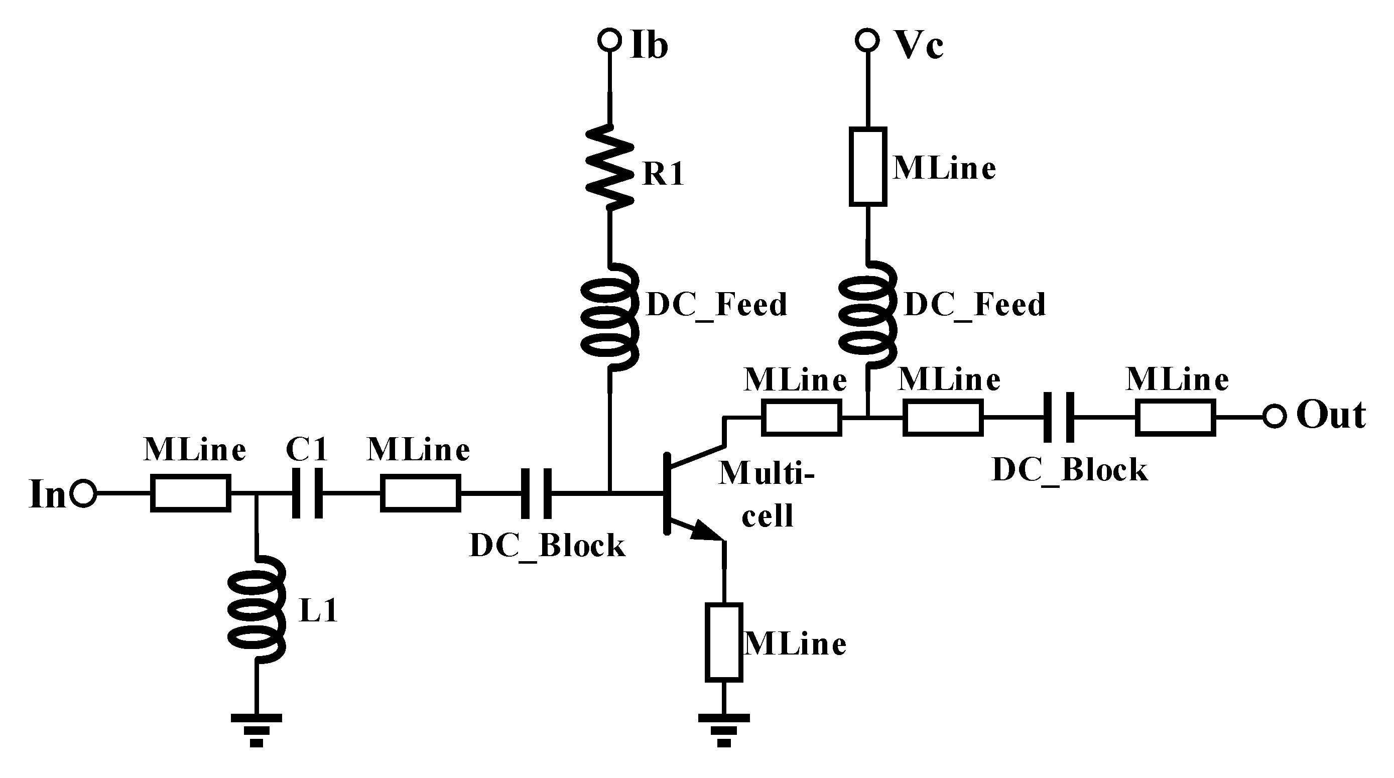
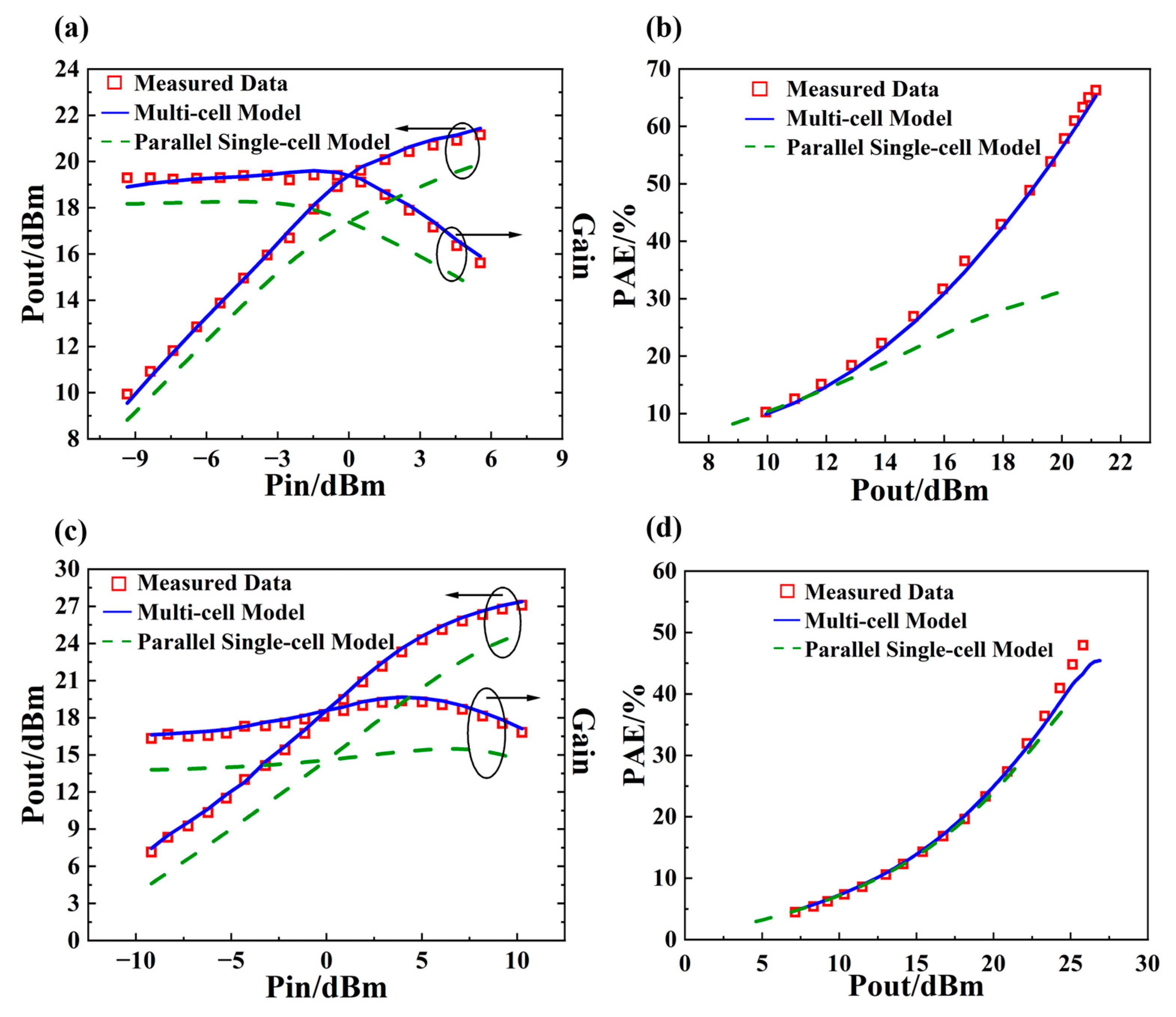
2.4. Multi-Cell Large-Signal Verification
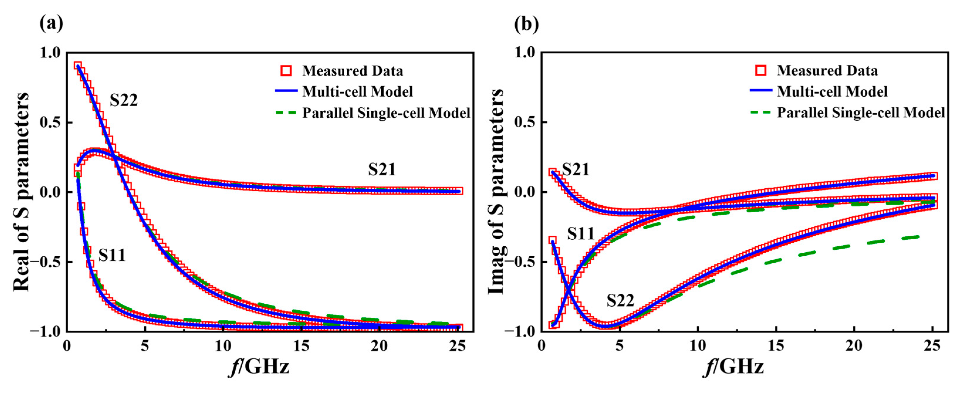
3. Experiment and Results
4. Conclusions
Author Contributions
Funding
Data Availability Statement
Acknowledgments
Conflicts of Interest
References
- Alizadeh, A.; Rowell, P.V.; Griffith, Z.; Urteaga, M.E.; Rodwell, M.J.W. A 78-mW 220-GHz Power Amplifier with Peak 18.4% PAE in 250-Nm InP HBT Technology. IEEE Trans. Microw. Theory Tech. 2024, 72, 5789–5798. [Google Scholar] [CrossRef]
- Griffith, Z.; Urteaga, M.; Rowell, P. A 220-GHz Power Amplifier With 60-mW Pout and 23.5% PAE in 130-Nm InP HBT. IEEE Microw. Wirel. Technol. Lett. 2024, 34, 431–434. [Google Scholar] [CrossRef]
- Nguyen, N.L.K.; Cui, C.; Nguyen, D.P.; Stameroff, A.N.; Pham, A.-V. A 7–115-GHz Distributed Amplifier with 24-dBm Output Power Using Quadruple-Stacked HBT in InP. IEEE Microw. Wirel. Technol. Lett. 2023, 33, 715–718. [Google Scholar] [CrossRef]
- Liu, W.L.; Yi, C.P.; Zhang, H.S.; Wang, Y.C.; Zhou, J.D.; Shi, C.Z.; Yang, S.H.; Lu, Y.; Deng, J.Y.; Ma, X.H.; et al. High Linear and Temperature Insensitive GaAs Power Amplifier Operating at 3.3–3.6 GHz Using a Multi-Feedback Branch Bias Circuit. IEEE Microw. Wirel. Technol. Lett. 2023, 33, 331–334. [Google Scholar] [CrossRef]
- Griffith, Z.; Urteaga, M.; Rowell, P.; Tran, L. A 150–175-GHz 30-dB S21 Power Amplifier with 125-mW Pout and 16.2% PAE Using InP HBT. IEEE Microw. Wirel. Compon. Lett. 2022, 32, 559–562. [Google Scholar] [CrossRef]
- Wan, C.; Zhang, H.; Zhao, Y.; Zeng, M.; Dong, J.; Li, L.; Wang, K. A Broadband SiGe HBT Cascode Power Amplifier Achieving Watt-Level Peak Output Power With 38.6% PAE and 90.9% Large-Signal Fractional Bandwidth. IEEE Trans. Circuits Syst. II 2022, 69, 4734–4738. [Google Scholar] [CrossRef]
- Radisic, V.; Scott, D.W.; Cavus, A.; Monier, C. 220-GHz High-Efficiency InP HBT Power Amplifiers. IEEE Trans. Microw. Theory Tech. 2014, 62, 3001–3005. [Google Scholar] [CrossRef]
- Lee, H.; Han, I.; Ju, I. A Highly Efficient, Linear Ka -Band SiGe HBT Cascode Power Amplifier with a Compact Lumped Element Coupled Line Impedance Inverting Balun. IEEE Trans. Microw. Theory Tech. 2024, 72, 5799–5808. [Google Scholar] [CrossRef]
- Wu, D.Y.; Chiu, Y.H.; Liu, Y.C.; Wu, C.Y.; Lour, W.S.; Wu, M.C. Monolithic Integration of GaAs-Based Darlington Cascode With Multifinger and Nonuniform Spacing Emitter. IEEE Trans. Electron Devices 2024, 71, 7358–7365. [Google Scholar] [CrossRef]
- Liu, M.; Ma, Z.; Ma, K.; Fu, H. A High-Power GaAs Amplifier with Coupled Bonding-Wires-Based Harmonic Control Output Matching Network. IEEE Microw. Wirel. Technol. Lett. 2023, 33, 1305–1308. [Google Scholar] [CrossRef]
- Chen, L.; Chen, L.; Zhu, H.; Gomez-Garcia, R.; Zhu, X. A Wideband Balanced Amplifier Using Edge-Coupled Quadrature Couplers in 0.13-Μm SiGe HBT Technology. IEEE Trans. Circuits Syst. I 2023, 70, 631–641. [Google Scholar] [CrossRef]
- Oh, H.; Shin, J.; Jeon, H.; Woo, Y.Y.; Hwang, K.C.; Lee, K.-Y.; Yang, Y. Broadband InGaP/GaAs HBT Doherty Power Amplifier IC Using Direct Interstage Power Division for Compact 5G NR Handset Module. IEEE Access 2023, 11, 25879–25892. [Google Scholar] [CrossRef]
- Zhou, Y.; Yu, P.P.; Gao, J.J. Radio-Frequency Modeling and Parameters Extraction of Multi-Cell MOSFET Device. J. Infrared Millim. Waves 2017, 36, 550–554. [Google Scholar] [CrossRef]
- Zhou, W.; Sun, L.; Liu, J.; Chen, Z.; Su, G.; Cheng, W.; Lu, H. Extraction and Verification of the Small-Signal Model for InP DHBTs in the 0.2–325 GHz Frequency Range. IEICE Electron. Express 2018, 15, 20180244. [Google Scholar] [CrossRef]
- Yang, X.; Sang, Q.; Wang, C.; Yu, M.; Zhao, Y. Development and Challenges of Reliability Modeling from Transistors to Circuits. IEEE J. Electron Devices Soc. 2023, 11, 179–189. [Google Scholar] [CrossRef]
- Wang, Z.; Xu, Z.; Liu, J.; Liu, J. Scalable AgilentHBT Model for GaAs HBTs. In Proceedings of the 2019 International Conference on Microwave and Millimeter Wave Technology (ICMMT), Guangzhou, China, 19–22 May 2019; pp. 1–3. [Google Scholar]
- Gonzalez-Teodoro, J.R.; Kindl, V.; Romero-Cadaval, E.; Asensi, R. Analysis of Skin Effect in Single Wire Resistance by Finite Element Methods. In Proceedings of the 2020 IEEE 14th International Conference on Compatibility, Power Electronics and Power Engineering (CPE-POWERENG), Setubal, Portugal, 8–10 July 2020; pp. 19–23. [Google Scholar]
- Gassab, O.; Xie, H.; Zhao, D.; Zhu, Y.; Du, S.; Xiao, D.; Yin, W.-Y. Efficient Modeling of Skin and Proximity Effects Over Ultrawide Frequency Range, Part I: Extraction of Transition Factors. IEEE Trans. Electromagn. Compat. 2024, 66, 1136–1152. [Google Scholar] [CrossRef]
- Zhang, A.; Zhang, Y.; Wang, B.; Gao, J. An approach to determine small-signal model parameters for InP HBT up to 110 GHz. Infrared Millim. Waves 2018, 37, 688–692. [Google Scholar] [CrossRef]
- Zhang, T.; Liu, J.; Xia, Y.; Zhang, Z. A Small Signal Model of the GaAs PHEMTs Considering the Skin Effect of Port Leads. Semicond. Technol. 2021, 46, 47–52. [Google Scholar] [CrossRef]
- Mangiavillano, C.; Kaineder, A.; Wagner, T.; Stelzer, A. A 240-GHz 4-TX 4-RX 2-D-MIMO FMCW Radar Transceiver in 130-Nm SiGe BiCMOS. IEEE Microw. Wirel. Technol. Lett. 2023, 33, 1239–1242. [Google Scholar] [CrossRef]
- Muller, M.; d’Alessandro, V.; Falk, S.; Weimer, C.; Jin, X.; Krattenmacher, M.; Kuthe, P.; Claus, M.; Schroter, M. Methods for Extracting the Temperature- and Power-Dependent Thermal Resistance for SiGe and III-V HBTs From DC Measurements: A Review and Comparison Across Technologies. IEEE Trans. Electron Devices 2022, 69, 4064–4074. [Google Scholar] [CrossRef]
- Gupta, A.; Nidhin, K.; Balanethiram, S.; Yadav, S.; Fregonese, S.; Zimmer, T.; Chakravorty, A. Optimizing Finger Spacing in Multifinger Bipolar Transistors for Minimal Electrothermal Coupling. IEEE Trans. Electron Devices 2022, 69, 6535–6540. [Google Scholar] [CrossRef]
- Gupta, A.; Nidhin, K.; Balanethiram, S.; D’Esposito, R.; Fregonese, S.; Zimmer, T.; Chakravorty, A. Extraction of True Finger Temperature from Measured Data in Multifinger Bipolar Transistors. IEEE Trans. Electron Devices 2021, 68, 1385–1388. [Google Scholar] [CrossRef]
- Luo, L.; Liu, J.; Wang, G.; Wu, Y. Small-Signal Modeling and Parameter Extraction Method for a Multigate GaAs pHEMT Switch. J. Semicond. 2020, 41, 032102. [Google Scholar] [CrossRef]


| Parameter | Values |
|---|---|
| RBx (Ω) | 0.119 |
| LBx (pH) | 27.86 |
| RCx (Ω) | 0.0158 |
| LCx (pH) | 30.9 |
| REx (Ω) | 0.0997 |
| LEx (pH) | 2.66 |
| CBn(n=1–5) (fF) | 0.158 |
| Ccen(n=1–6) (fF) | 21.8 |
| RBinm(n=1–6; m=1–2) (Ω) | 0.455 |
| LBinm(n=1–6; m=1–2) (pH) | 3.97 |
| RCin(n=2–5) (Ω) | 0.069 |
| LCin(n=2–5) (pH) | 18.82 |
| RCin(n=1; 6) (Ω) | 0.0345 |
| LCin(n=1; 6) (pH) | 9.41 |
| Model | S11 | S22 | S21 | S12 |
|---|---|---|---|---|
| Extracting external parasitic | 1.37% | 1.66% | 5.17% | 5.17% |
| Directly paralleling | 12.11% | 12.63% | 17.99% | 18.00% |
Disclaimer/Publisher’s Note: The statements, opinions and data contained in all publications are solely those of the individual author(s) and contributor(s) and not of MDPI and/or the editor(s). MDPI and/or the editor(s) disclaim responsibility for any injury to people or property resulting from any ideas, methods, instructions or products referred to in the content. |
© 2025 by the authors. Licensee MDPI, Basel, Switzerland. This article is an open access article distributed under the terms and conditions of the Creative Commons Attribution (CC BY) license (https://creativecommons.org/licenses/by/4.0/).
Share and Cite
Zhao, H.; Liu, J.; Rong, T.; Fan, S.; Chen, Z.; Wang, J. Modeling of Multi-Cell HBT Device Based on Device Structure. Micromachines 2025, 16, 433. https://doi.org/10.3390/mi16040433
Zhao H, Liu J, Rong T, Fan S, Chen Z, Wang J. Modeling of Multi-Cell HBT Device Based on Device Structure. Micromachines. 2025; 16(4):433. https://doi.org/10.3390/mi16040433
Chicago/Turabian StyleZhao, Haoyi, Jun Liu, Tao Rong, Shiyue Fan, Zhanfei Chen, and Junchao Wang. 2025. "Modeling of Multi-Cell HBT Device Based on Device Structure" Micromachines 16, no. 4: 433. https://doi.org/10.3390/mi16040433
APA StyleZhao, H., Liu, J., Rong, T., Fan, S., Chen, Z., & Wang, J. (2025). Modeling of Multi-Cell HBT Device Based on Device Structure. Micromachines, 16(4), 433. https://doi.org/10.3390/mi16040433