1. Introduction
Microfluidic chips (chips) represent a dynamic and continually advancing area of research that offers numerous advantages to both chemical and biological investigations. These include minimizing the quantity of samples and reagents required, shortening experimental durations, and facilitating the creation of in vivo-like conditions [
1]. The current technologies for fabricating microfluidic chips mainly include the LIGA technique [
2], photolithography [
3], laser ablation [
4], and 3D printing [
5], among others. At present, three-dimensional (3D) printing technology, also known as additive manufacturing technology, has the advantage of rapid prototyping to reduce costs and has become a crucial technique for rapidly prototyping microfluidic devices [
6]. Various 3D-printed technologies have been explored for the fabrication of microfluidic devices, including stereolithography (SLA) [
7], inkjet printing [
8], multi-jet printing [
9], and fused deposition modeling (FDM) [
10]. Khoo et al. proposed a rapid prototyping protocol to fabricate thermoplastic devices from an SLA 3D printing template through intermediate steps akin to those employed in soft lithography. This process was applied to the design of self-operating capillary circuits and is well suited for deployment in low-cost decentralized assays [
11].
Compared to whole 3D printing processing methods, fused deposition modeling (FDM) technology, with faster prototyping, shorter lead times for manufacturing, and lower production costs, has gained considerable attention. Fused deposition modeling (FDM) is an additive manufacturing technology commonly used for modeling, prototyping, and production applications. FDM works using an additive principle by laying down material in layers, and a plastic filament is unwound from a coil and supplies material to produce a part. PMMA, also known as acrylic glass or acrylic, is a transparent, lightweight, and durable thermoplastic with excellent optical clarity and weather resistance [
12]. Its application in microfluidic systems offers numerous advantages, including ease of fabrication, biocompatibility, and the ability to create complex, three-dimensional structures. Furthermore, the use of PMMA in microfluidic systems has been shown to provide excellent optical clarity, making it suitable for imaging and analysis applications.
Scientific research has demonstrated the feasibility and potential of 3D printing PMMA microfluidic chips. Urrios et al.’s study showed that PMMA-based microfluidic devices could be used for cell culture applications, with cells growing well within the devices [
13]. Bressan et al. presented a solvent bonding method of polymethyl methacrylate and acrylonitrile butadiene styrene (ABS) thermoplastic materials for the creation of optically detectable 3D-printed microfluidic devices [
14]. Kotz et al. demonstrated that using FDM, microfluidic chips with a minimum channel cross-section of ~300 µm can be printed and a variety of different channel geometries and mixer structures are shown. Researchers further demonstrate that protein patterns can be generated within previously printed microfluidic chips by employing a method of photobleaching [
15]. Thana et al. demonstrated that 3D printers with three-dimensional (3D) printing, computer numerical control (CNC) milling, and laser engraving technology were an effective strategy for creating microfluidic devices and an easier and more economical alternative to, for instance, conventional photolithography [
16]. Plastic microfluidic chips with engraved microchannel structures or micro-structured plastic molds for casting polydimethylsiloxane (PDMS) chips with microchannel imprints were produced. Akbari et al. discussed the microfabrication approaches used for creating inertial microchannels, including photolithography, xerography, laser cutting, micromachining, microwire technique, etching, hot embossing, 3D printing, and injection molding [
17]. The advantages and disadvantages of these methods were also discussed. Tsao et al. gave a short overview of polymer microfabrication methods for microfluidics and discussed current challenges and future opportunities for research in polymer microfluidics fabrication [
18]. Gyimah et al. evaluated the potential of the large-scale application of 3D-printed microfluidics [
19]. Cutuli et al. proposed a multi-objective polydimethylsiloxane (PDMS) micro-optofluidic (MoF) device suitably designed and manufactured through a 3D-printed-based master–slave approach [
20].
In conclusion, FDM 3D-printed technology with a layer-by-layer extrusion mechanism resulted in channel resolutions typically >200 μm, which struggled to meet the sub-200 μm requirements for advanced microfluidics applications. Surface roughness, caused by filament stacking, led to fluid leakage or inefficient flow control. While the FDM PMMA microfluidic chip faced challenges in resolution and material performance, its low cost and adaptability made it indispensable for research and niche applications. Through systematic optimization of FDM 3D-printed parameters, this work developed a low-cost fabrication process for PMMA microfluidic chips capable of producing 200 μm-scale channels. The optimized chips exhibited enhanced mechanical stability, reduced thermal deformation, and reliable fluidic performance, achieved by effectively mitigating clogging and leakage risks.
This paper presents the design and fabrication of FDM 3D-printed PMMA microfluidic devices for chemical reaction engineering. The FDM 3D-printed parameters are optimized through iterative experiments, and a single-step printing molding technique is developed. This integrated approach simplifies the fabrication workflow by eliminating the need for post-printing bonding processes. Firstly, numerical simulation is integrated with experimental trials to analyze thermal stress evolution during FDM 3D-printed PMMA, enabling the identification of critical printing parameters that mitigate warping and delamination through optimized thermomechanical control. Secondly, an L9(33) orthogonal experimental design is implemented to systematically optimize printing parameters, resulting in a significant reduction in the fabricated microchannel surface roughness. Thirdly, the microreactor structure is designed and fabricated via a single-step integrated 3D-printed process, utilizing optimized parameters to achieve monolithic construction with enhanced structural integrity. Finally, a set of chemical reactions between copper ions and ammonium hydroxide are conducted, resulting in a blue-colored copper hydroxide solution.
2. Materials and Methods
2.1. Three-Dimensional Printing Materials
In the experiment, PMMA as an organic polymer material was studied. The polymer substrate possessed characteristics of high transparency, excellent toughness and very good dimensional stability. The density of PMMA was 1.18 g/cm3, and the temperature of glass transition is 104 °C. The transmittance of PMMA was about 92% in infrared spectral range. PMMA was well-suited for 3D printing owing to its thermoplastic properties. The material was melted and extruded via fused deposition modeling (FDM) systems, enabling the fabrication of high-precision microfluidic architectures with intricate geometries. In this experiment, PMMA filament was purchased from Chinese shopping website.
2.2. FDM 3D Printing System
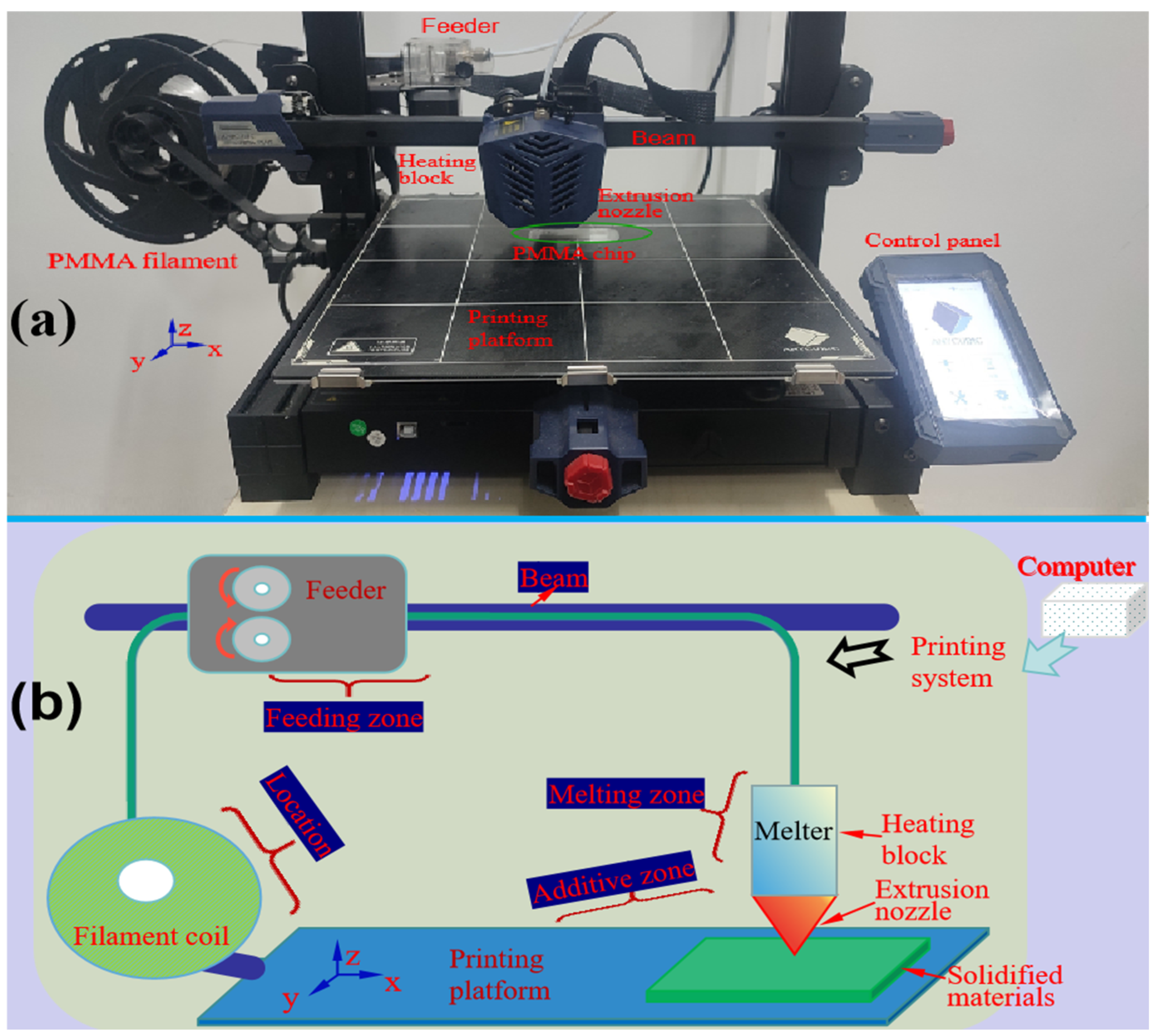
During the 3D printer printing the target parts, all designs were created using SolidWorks design software 2022 and exported as STL files in computer. In this research, the STL files were imported into JGcreat 4.8.6 for the slicing process. The microchannel structure was designed in SolidWorks software v2022 and then imported into slicing software for processing. The relevant machining parameters were set in the slicing software, which can automatically complete the trajectory data extraction, trajectory planning, simulation, and interference check. The FDM printer Anycubic Kobra Plus (Anycubic Technology, Shenzhen, China) was used for printing.
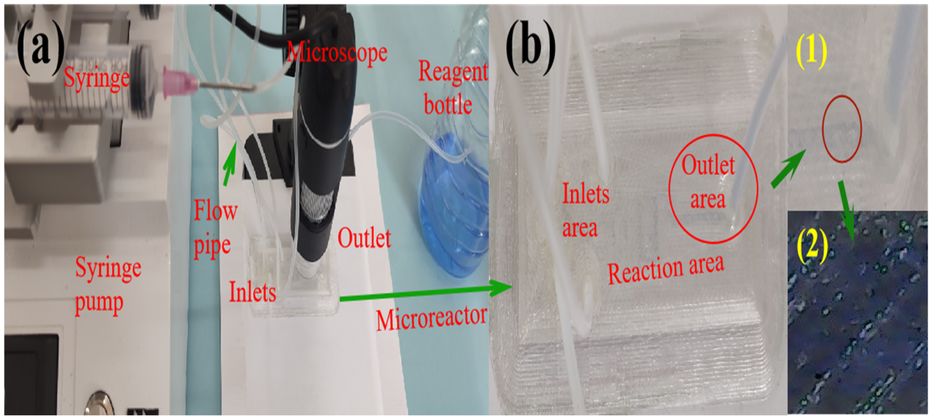
Figure 1a shows the structure diagram of FDM 3D-printed process.
Figure 1b shows the schematic diagram of FDM 3D-printed process. The 3D printer consisted of a location zone, a feeding zone, a melting zone and an additive manufacturing zone. A beam was mounted on a stabilizing frame that allowed movement along the
x-,
y-, and
z-axes. The positioning zone served to initially position the filament material, ensuring that it could enter the feeding zone accurately and smoothly. The feeding zone consisted of a drive gear and an idler pulley with an integrated bearing, where a precisely calibrated gap was maintained between the two components to ensure controlled filament traction. The melting zone consisted of an extrusion nozzle and a heating block with thermal insulation layer. Within the heating block, filaments were melted in a pressurized chamber via a piston-driven mechanism, which extrudes the molten material through the nozzle. The additive manufacturing zone included workbench and workpiece. The additive manufacturing process was performed on workbench, where molten filament was extruded from nozzle. The melt zone was mounted on a three-axis gantry system, which precisely controlled movement along the
x-,
y-, and
z-axes. The
z-direction determined the thickness of each printed layer. On the 3D printer, the control panel enabled functions to suspend, start, and stop the printing process.
2.3. Finite Element Analysis
During the preliminary phase of process development, FDM 3D printing of PMMA filament was simulated using COMSOL Multiphysics software v5.5, a finite element analysis software platform for multiphysics computational modeling. Heat transfer in solids interface was used to simulate heat transfer by conduction and convection. A solid model was active by default on the simulation domains. The temperature equation defined in the solid domains was governed by the differential form of Fourier’s law. There were two equations as calculative tools in the simulation.
The simulation was explained by the following Fourier Heat equations:
where
ρ represents density,
Cp stands for specific heat capacity,
T denotes temperature,
K is the thermal conductivity coefficient,
Q signifies heat flux, and
Qted is the thermoelastic effect.
In order to obtain a stable thermodynamic model, a point heat source was set with the equation.
where
ρ is the density of the heat-conducting medium and
c is the specific heat capacity of the heat-conducting medium.
This time-dependent study was supported in three dimensions, and PMMA material was used for the simulation process. To reduce computational load while ensuring accuracy, this simulation focused on a single-layer model featuring a cuboid of 0.1 mm and divided the finite element mesh into ultra-fine mesh elements.
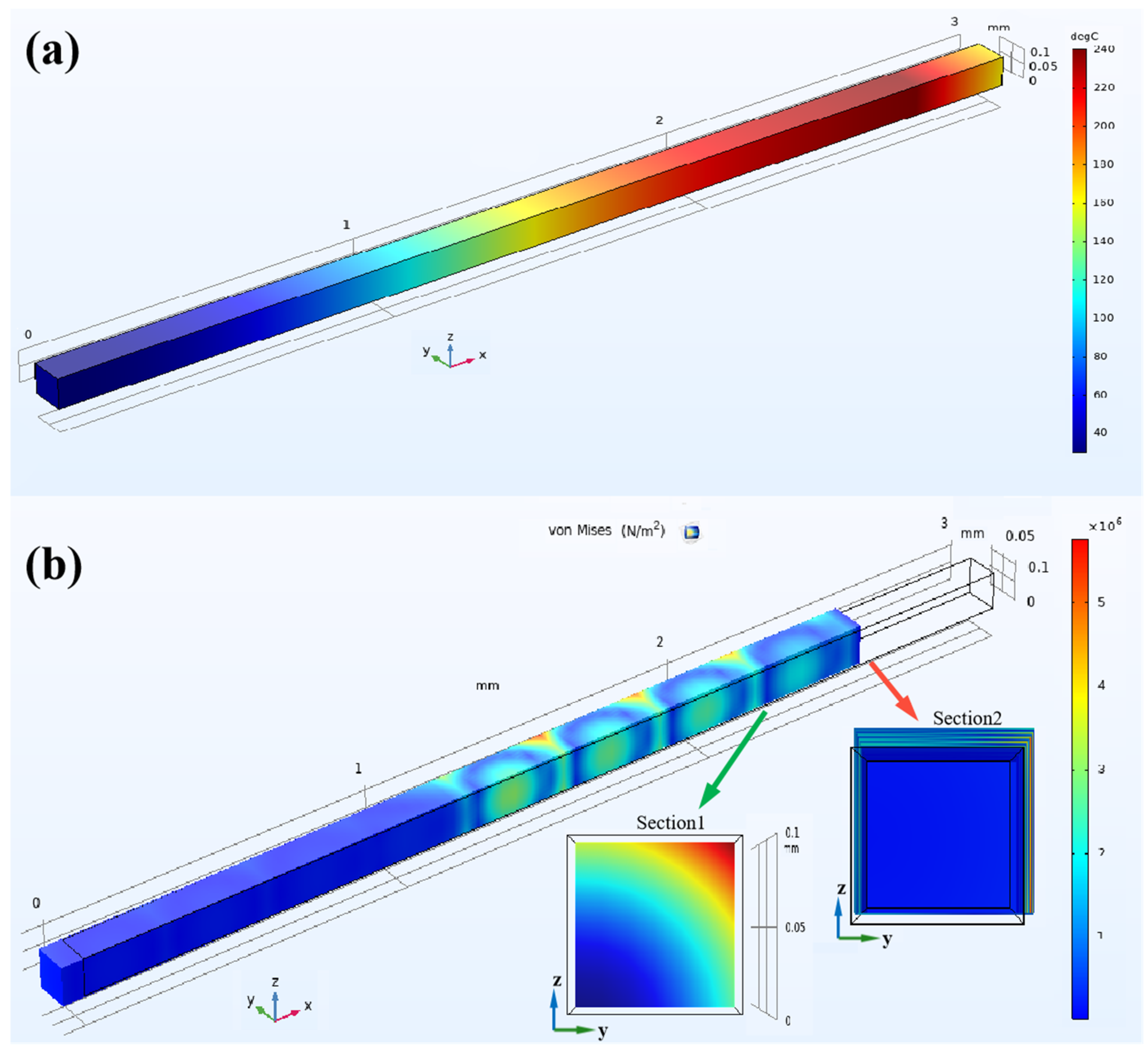
Figure 2 reflects the actual temperature and thermal stress distribution in the FDM 3D-printed PMMA process. The actual temperature distribution on the PMMA printed surface at 0.6 s is shown in
Figure 2a. In the diagram, the range from 0 mm to 3 mm represented the printing direction of the material. The high-temperature area moved along this printing direction, and the already printed sections rapidly cooled down to room temperature as printing progressed. During the layer-by-layer additive manufacturing process, heat accumulation occurred due to conductive thermal transfer between material layers, while non-uniform temperature gradients and differential thermal expansion induced residual stresses within the deposited structure.
Due to heat transfer, thermal stress arose on the surface of the printing layer, as illustrated in
Figure 2b. The color legend on the right indicated the distribution of the Von Mises stress, which arose from thermal conduction and heat accumulation during the additive manufacturing process. The thermal stress distribution analysis revealed the progressive evolution of internal stresses during the additive manufacturing process, with particular emphasis on scenarios characterized by minimal substrate adhesion. Temporal analysis revealed that residual thermal stresses in the initially deposited layer were observed to progressively diminish, while a tripartite stress concentration configuration developed within newly deposited layers during subsequent manufacturing phases. The green arrow pointed to the side view
Section 1, which not only delineated the directional stress gradient characteristics in the
zy-plane but also revealed the vector alignment between principal thermal stress concentrations and the resultant thermo-mechanical load vector. According to the cross-sectional analysis of the stress gradient, a gradual decrease in magnitude was observed from the upper right corner to the lower left corner of the
zy-plane, with the maximum stress concentration located in the upper right region. The red arrow highlighted
Section 2 in the side view aligned with the
x-axis. In this section, the black outline corresponded to the designed contour, whereas the numerically simulated contour deviated toward the
zy-plane, suggesting potential thermal–structural coupling effects.
2.4. Discussion of 3D Printing Parameter
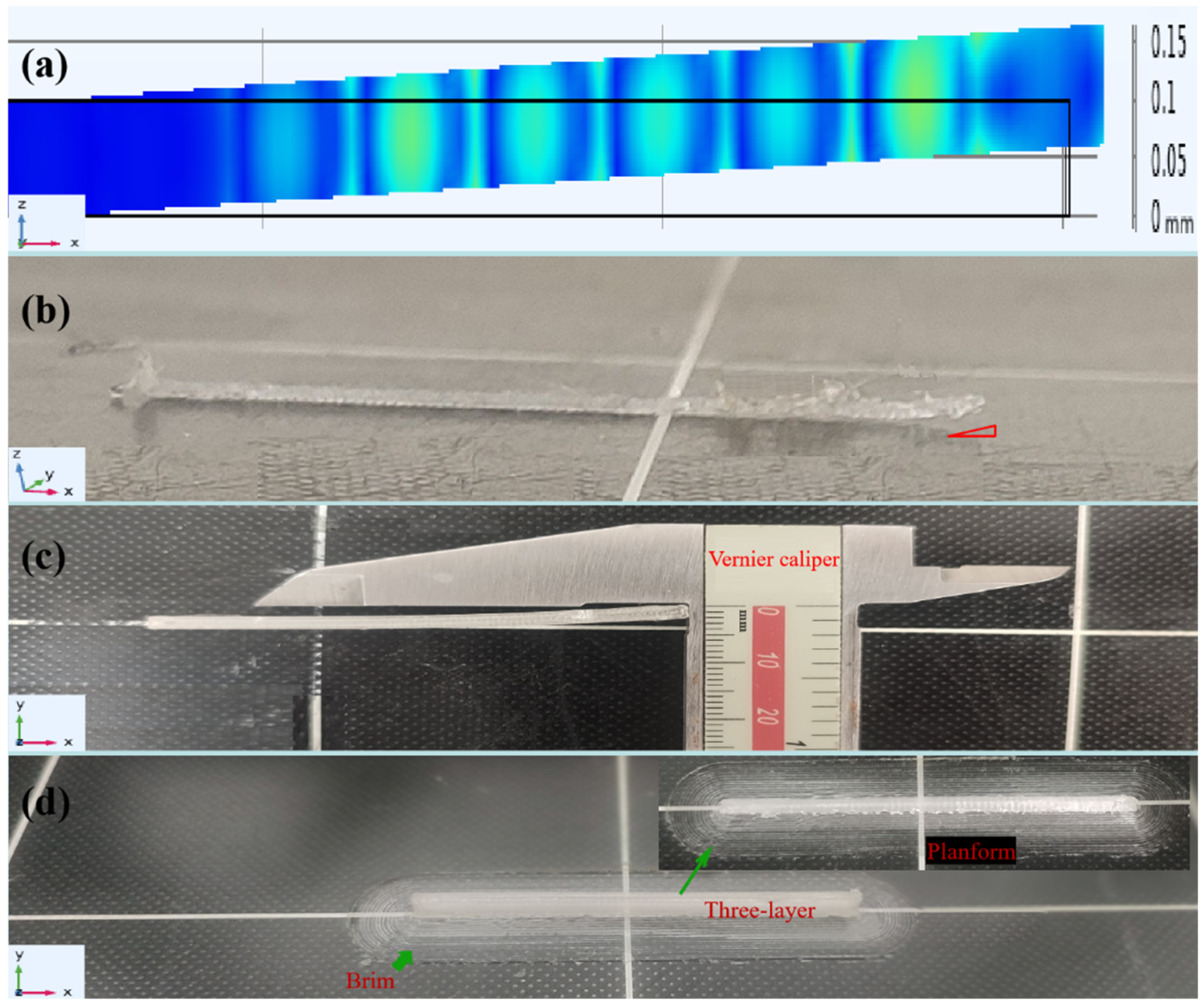
Figure 3 presents a comparative analysis of warping deformation along the
xz-axis in PMMA printed materials between experimental measurements and numerical simulations at matched spatial coordinates. The corresponding numerical simulations and experimental measurements under identical printing parameters are presented in
Figure 3a and
Figure 3b, respectively. Both figures exhibited similar
z-axis warping trends in the PMMA material, with deformation increasing progressively during printing.
Figure 3c illustrates the
y-axis warping deformation of PMMA material after three-layer deposition along a vertical build path. A vernier caliper with precision markings was used to quantify the maximum warping displacement as 0.2 mm, measured relative to the reference horizontal line on the printing platform. The observed deformation direction aligned quantitatively with the simulated thermal stress gradient vector field (
Figure 2b,
Section 1, green arrow), confirming the thermomechanical coupling effects during printing.
To mitigate warping and interlayer delamination, a single-factor experimental design was implemented to systematically identify critical process parameters.
Figure 3d shows the defect-free microstructure of the PMMA specimen achieved through the optimized printing strategy. Horizontal alignment of the PMMA structure along the bed's reference line was achieved through precise temperature control of the build platform. The experimental results showed the printing effect of PMMA material was optimal without warping and delamination issues when the printing platform temperature was set to 95 °C. Furthermore, the printing platform attachment type was also one of the key factors to enhance the stability of printed objects. Implementing a brim attachment type around the model base improved mechanical stability and reduced thermal contraction stresses. These discoveries were crucial for ensuring the accuracy and integrity of the printed parts.
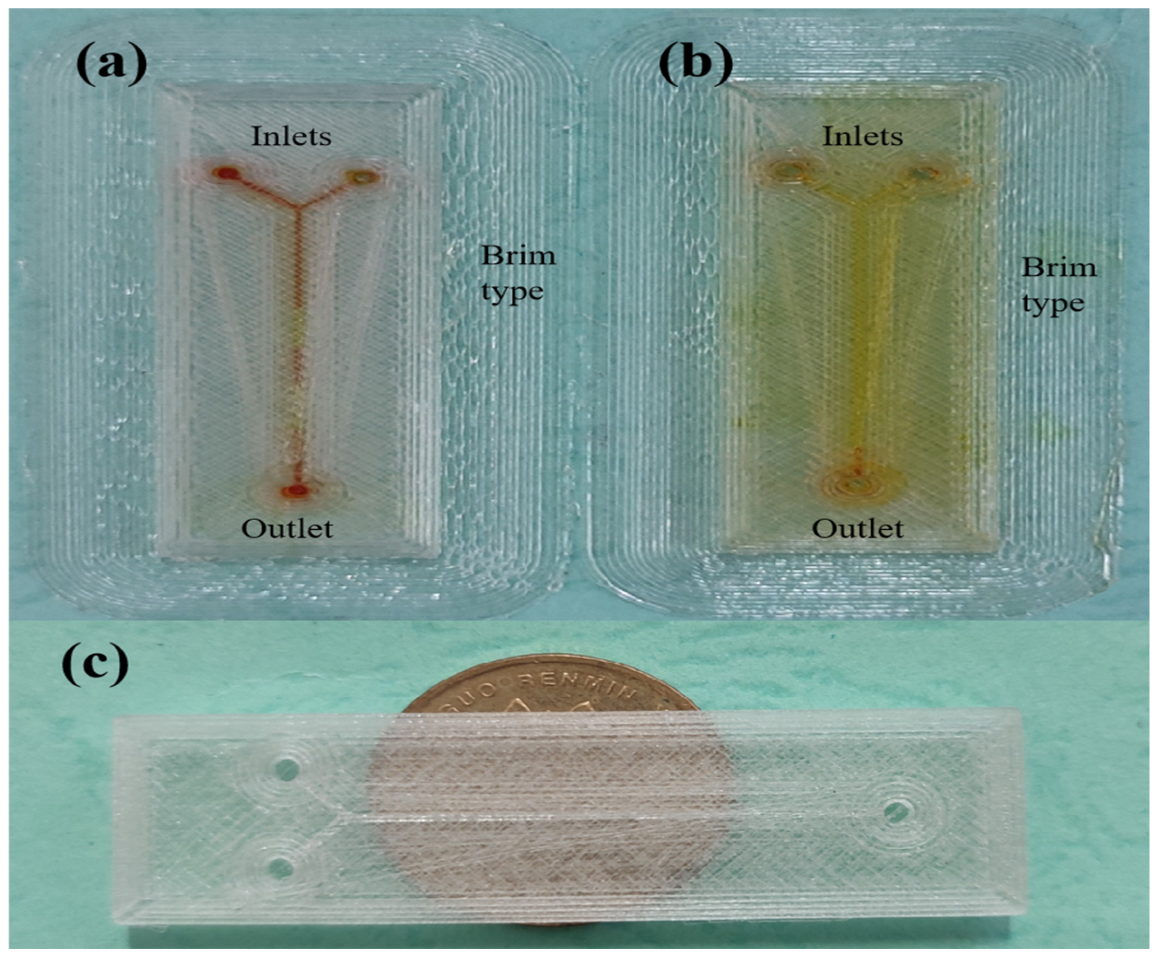
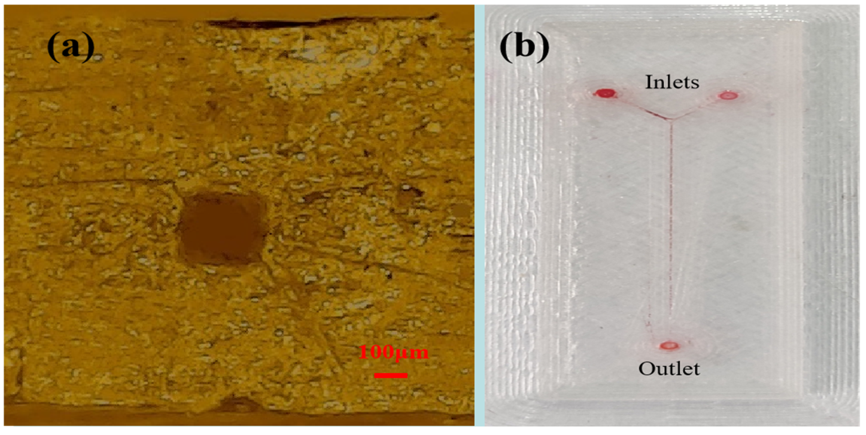
Figure 4 shows side leakage and transparency test results for samples produced through a single printing molding technique with different processing parameters. A single printing molding technique bypassed traditional chip bonding and streamlined fabrication processes. The sample microfluidic chip had dimensions of 50 mm in length, 2 mm in thickness, and 15 mm in width in this test. The cross-section of the designed microchannel was a square with a side length of 0.3 mm. This work ultimately revealed that while the infill pattern was a crucial factor in preventing leakage from the sealed chip during printing, other parameters, including nozzle extrusion temperature, layer height, and print platform temperature, also contributed to maintaining structural integrity. The gyroid, a triply periodic minimal surface (TPMS) structure, exhibited outstanding physical properties. Compared to other twelve structural patterns (e.g., triangular, square, and hexagonal), the structure could significantly enhance strength and increase specific surface area. Red or yellow ink was employed in this experiment owing to their high visual contrast under optical monitoring.
Figure 4a depicts the state of the chip without leakage, and
Figure 4b shows the state of the chip with leakage. During the printing process, an underlying layer was added for enhancing chip stability.
Figure 4c shows the optical transparency analysis of a microfluidic chip sample with a thickness of 2 mm alongside its surface morphological characterization. This was a comparison photograph between the microreactor and a fifty-cent yuan coin, which clearly showed the transparency of the 3D-printed PMMA microfluidic chip.
Based on the above discussion of experimental parameters and PMMA material properties, the parameters of the FDM 3D-printed process were as follows: a layer height of 0.1 mm, an infill of 100%, a printing speed of 30 mm/s, a nozzle temperature of 220 °C, a fill pattern of gyroid, a printing platform attachment type of brim, and a platform temperature of 95 °C. Printing parameter optimization enabled the fabrication of PMMA microchannels via 3D printing, achieving a minimum channel width of 200 μm. The thickness of the microfluidic chip was set to 1.5 mm to ensure clearer transparency. The channel cross-section with the size of 200 μm was a similar rectangle-shaped design, as shown in
Figure 5a. This minor deviation was observed and was attributed to the phase transition phenomenon involving melting and re-solidification of the materials. The printing material underwent shrinkage during the solidification process, which led to a dimension change of microchannels. At the micrometer scale, even minor changes of material flowability could result in discrepancies of cross-section between the design and the printed microchannel. Printing of channels with both width and height below 200 μm resulted in partial clogging and was therefore not further investigated.
Figure 5b shows that it did not leak and clog. Red ink was employed in this experiment owing to its high visual contrast under optical monitoring.
2.5. Roughness Analysis of Orthogonal Method
During FDM 3D printing of a PMMA microfluidic chip, anisotropic thermal expansion coefficients of PMMA during heating, extrusion, and cooling processes induced molecular chain orientation and cooling rate gradients. These factors led to non-uniform material shrinkage, causing dimensional deviation and blockage of microchannel cross-section. Additionally, the instantaneous temperature difference between the molten PMMA layer (upper) and the solidified layer (lower) during sequential deposition could reach 120 °C, generating an inhomogeneous thermal stress field. The rapid cooling-induced shrinkage of the upper layer imposed tensile stress on the underlying layers, resulting in interlayer delamination or microcrack formation, which compromised the mechanical stability of the chip. The thermo-mechanical coupling behavior during 3D printing PMMA was critical for improving microfluidic chip precision. Addressing these challenges requires an optimized processing parameter to balance manufacturing efficiency with functional reliability of the device.
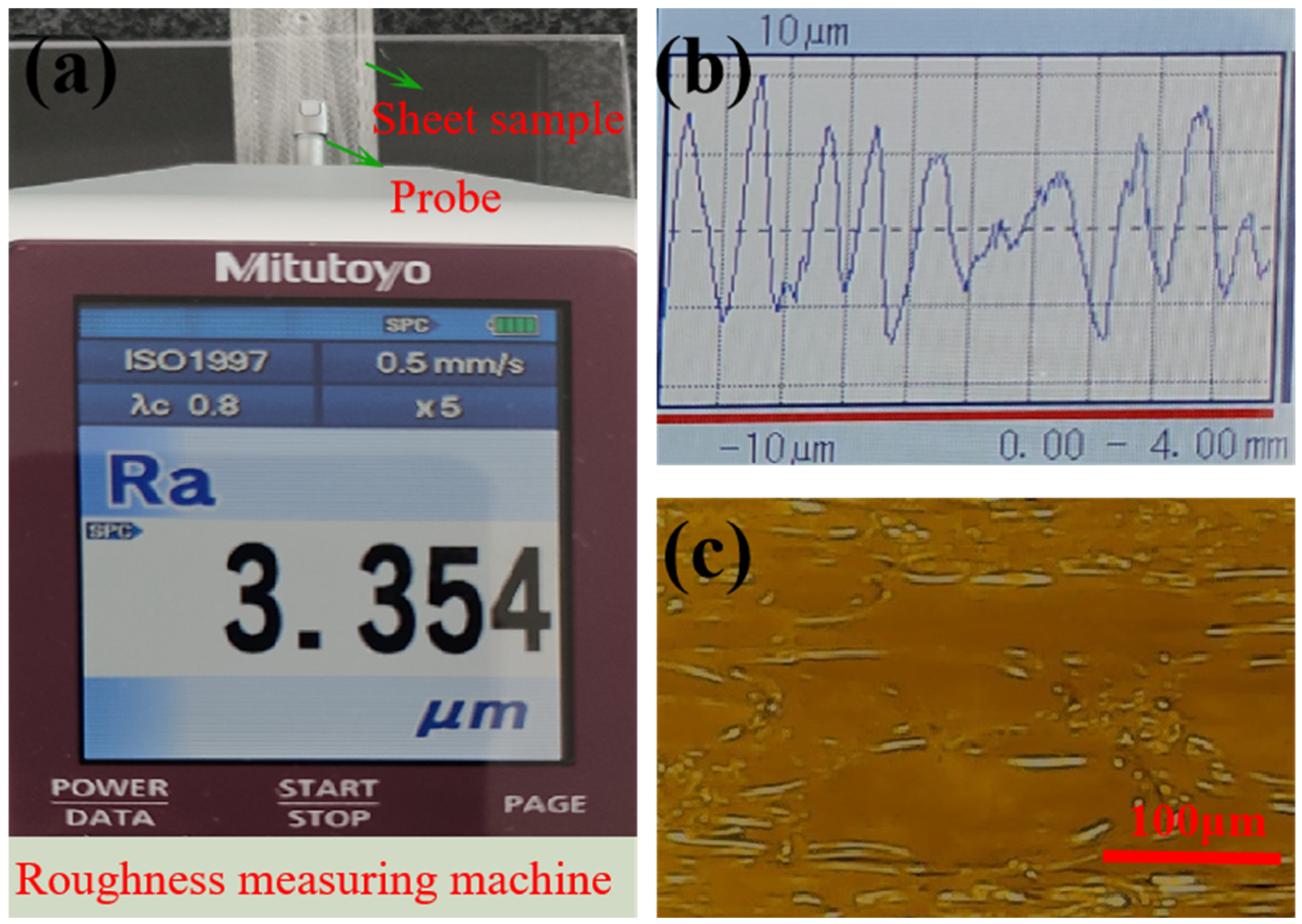
The impact of microchannel surface roughness on a microfluidic chip was multifaceted, encompassing flow speed, flow state, reaction efficiency, mixing effect, chip performance and stability, as well as detection results and accuracy. Therefore, during the design and fabrication of a microfluidic chip, it was necessary to strictly control the surface roughness to ensure that the performance and stability of the chip meet the practical application requirements. A set of experiments on the surface roughness of microchannels using a single 3D-printed technique were performed. In order to ensure the accuracy of measuring data, the printing PMMA microchannels were cleaned by the ultrasonic cleaning machine. After achieving the cleaning microchannel, ten measurement points were selected in each microchannel. The data of roughness were obtained by the roughness measuring machine with a probe.
Figure 6 shows the experimental system of measuring roughness and the micrograph of the PMMA microchannel profile. The roughness measuring machine selected is the SJ-210 of the Mitotoyo Company (Kawasaki City, Kanagawa Prefecture, Japan), and the testing standard is the international roughness measurement standard (ISO1997) [
21].
Figure 6a,b show the roughness value and roughness waviness of the microchannel profile using the roughness measuring machine. The roughness value (
Ra) was 3.354 μm. Due to the instability of the experiment, the experimental data have great volatility. The final data were the average of ten datasets.
Figure 6c shows the microchannel profile was not regular using metallographic microscopy.
For convenience, the optimal conditions were obtained by a few experiments using the orthogonal experiment method. The nozzle temperature, printing speed, and layer height are defined as the main factors to influence the microchannel profile in the experiment. A L9(3
3) 3D-printed orthogonal array experiment using orthogonal array experimental factors was performed. The orthogonal levels and factors were listed in
Table 1.
Table 2 showed the corresponding parameter of the experiment of each group and the factors response.
The average values of ten sets of microchannel roughness was obtained through microscopic testing and are summarized in
Table 2. The processing stability was defined as follows:
where S
imax was the maximum roughness of the microchannel profile and S
imin was the minimum roughness of the microchannel.
T1,
T2, and
T3 respectively indicated the average of factors in each level. The computational formula was defined as follows:
where
i is the number of levels and
l is the number of factors.
R represented the sensitivity of the various factors and was calculated by Equation (5).
where
Tmax and
Tmin showed maximum and minimum in the whole array, respectively.
In
Table 2, range
R represented the influencing results of all factors. The influence of maximum and minimum was nozzle temperature and layer height among all parameters, respectively.
In order to clearly express the effect of factors in
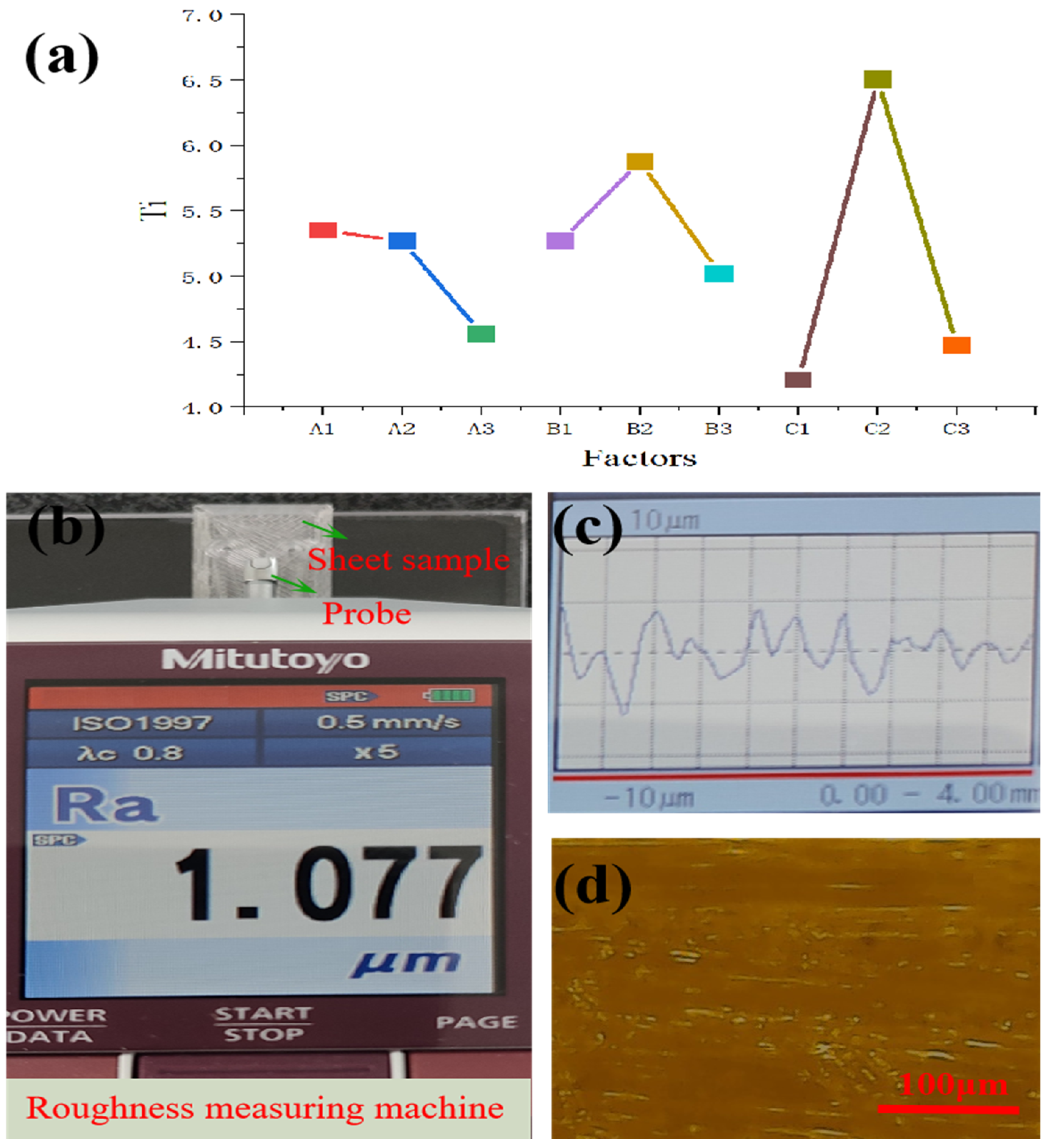
Table 2, a factor response figure was presented.
Figure 7a shows a factor response figure. In the figure, the line was steeper, and the influence of the factor was greater. The line representing layer height was close to the vertical, so it was the most sensitive factor for processing improvement. The level combination of better 3D-printed parameters in the experiment was A3B3C1. The layer height was 0.1 mm, the printing speed was 35 mm/s, and the nozzle temperature was 220 °C. According to the result,
Figure 7b and
Figure 7c, respectively, present the surface roughness value and waviness of PMMA microchannel fabricated with optimized 3D printing parameters in the measuring system. The roughness of the microchannel profile was 1.077 μm using the roughness measuring machine.
Figure 7d shows that the micrograph of the microchannel profile with optimized 3D-printed parameters was regular and smooth using metallographic microscopy.
4. Conclusions
A 3D-printing technique with the advantages of low cost, rapid prototyping, and the creation of complex structures has garnered significant attention for the manufacture of microfluidic devices. In this work, the processing technology of PMMA microfluidic chips using a commercial FDM 3D printer was investigated, and the chemical experiment was performed in a 3D-printed PMMA microreactor.
The finite element numerical analysis method was used to predict the change of thermal stress in the process of 3D-printed PMMA material. The results of numerical modeling showed that the printing platform temperature was one of the critical printing parameters for preventing warping and delamination in the experiment. The experimental results showed that the printing performance of the PMMA material was optimal, with no warping or delamination, when the platform temperature was set to 95 °C and the attachment type was configured as brim. This design effectively prevented the PMMA materials from moving or deforming during printing, thereby improving both print accuracy and success rate. During fabrication, a single-step 3D-printing technique was used to produce microfluidic chips exhibiting high optical clarity, with embedded channels featuring square cross-sections of 200 μm. The microchannel exhibited no clogging or leakage. Through orthogonal experiments, it was revealed that nozzle temperature is an important factor affecting the microchannel profile roughness. Optimized 3D-printed parameters were obtained to reduce the microchannel profile roughness to Ra1.077 μm.
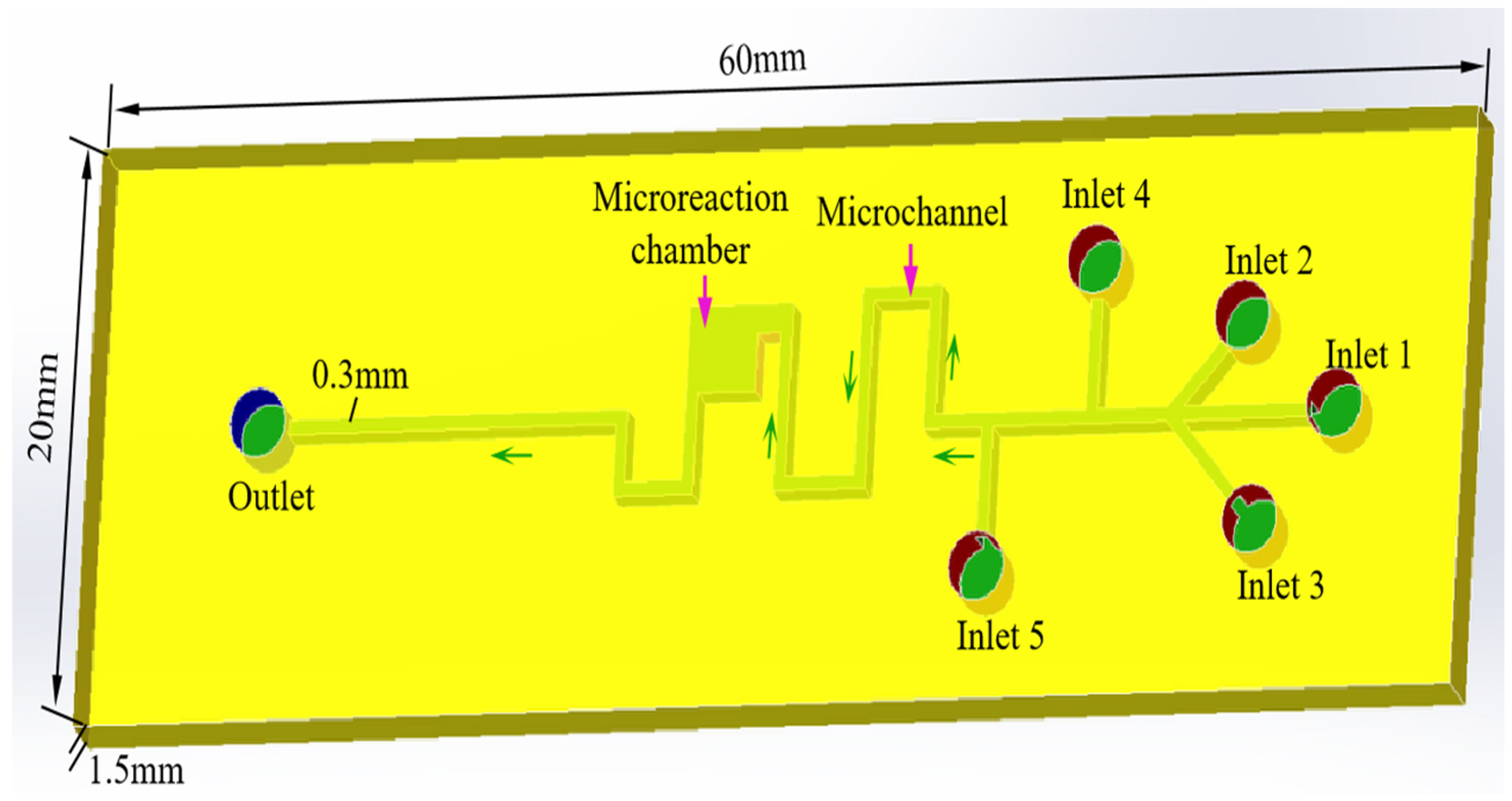
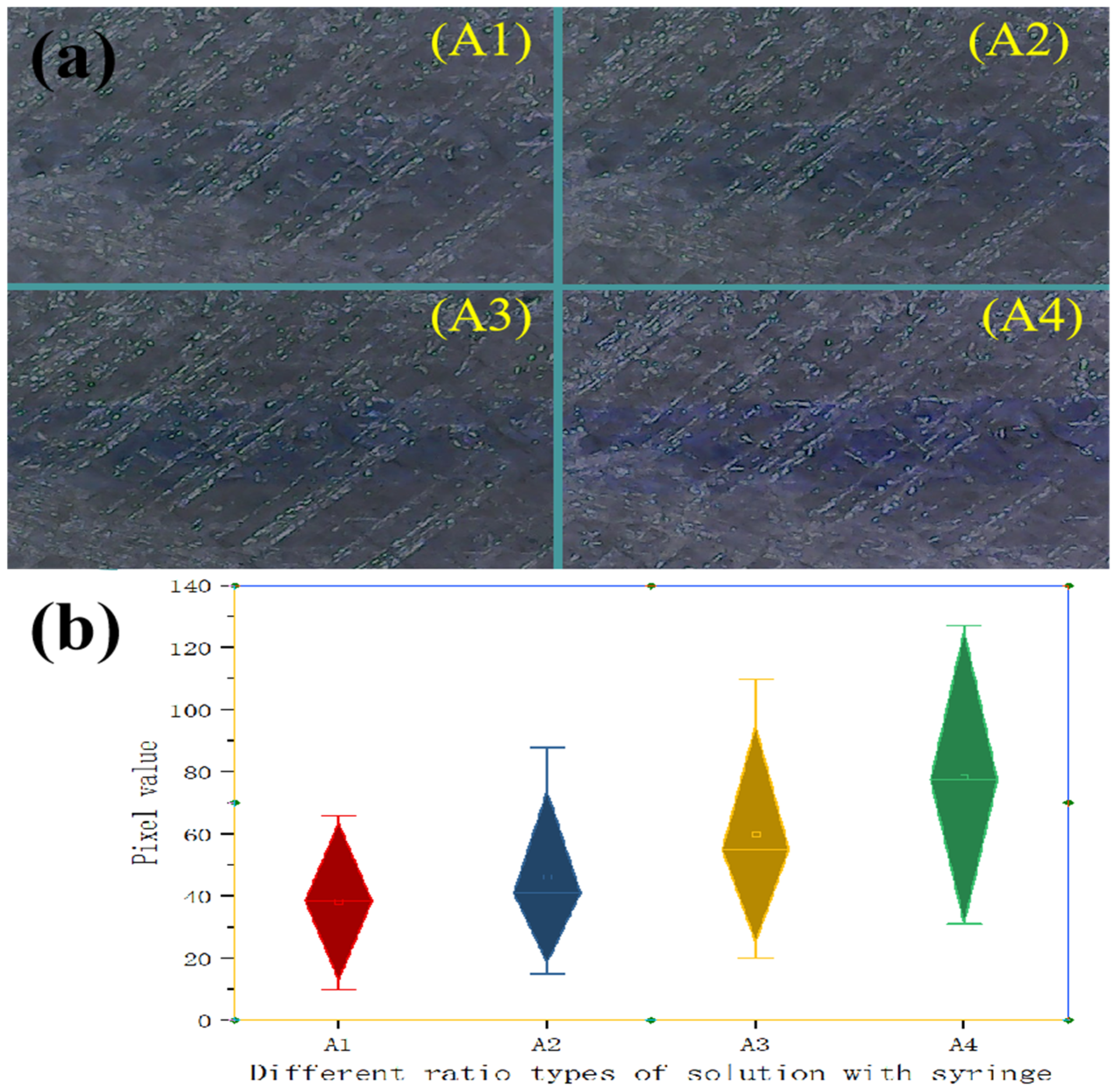
Excessive copper ions in water or food posed health risks to humans. A chemical reaction system based on microfluidic chips for copper ions and ammonium hydroxide has been designed and prepared using optimized 3D-printed parameters. To obtain copper hydroxide solutions with varying shades of blue, the microreactor was equipped with five inlets, each corresponding to a syringe. All syringes contained the same molar mass of sample solution. By adjusting the combination of ammonium hydroxide and copper ion solutions in five syringes, varying shades of blue in the copper hydroxide product were observed at the outlet. Ultimately, a box color data graph of copper hydroxide was presented. This work provided a convenient, inexpensive, and rapid method for future heavy metal detection in water. Future works will focus on integrating 3D-printed water quality detection chips with smartphones and promoting high-quality development of microfluidic chips.


