Abstract
In this work, the electrical properties of the Ga2O3 Schottky barrier diodes (SBDs) using W/Au as the Schottky metal were investigated. Due to the 450 °C post-anode annealing (PAA), the reduced oxygen vacancy defects on the β-Ga2O3 surface resulted in the improvement in the forward characteristics of the W/Au Ga2O3 Schottky diode, and the breakdown voltage was significantly enhanced, increasing by 56.25% from 400 V to 625 V after PAA treatment. Additionally, the temperature dependence of barrier heights and ideality factors was analyzed using the thermionic emission (TE) model combined with a Gaussian distribution of barrier heights. Post-annealing reduced the apparent barrier height standard deviation from 112 meV to 92 meV, indicating a decrease in barrier height fluctuations. And the modified Richardson constants calculated for the as-deposited and annealed samples were in close agreement with the theoretical value, demonstrating that the barrier inhomogeneity of the W/Au Ga2O3 SBDs can be accurately explained using the TE model with a Gaussian distribution of barrier heights.
1. Introduction
With the development of technology, there is a growing demand for higher operating voltages, ambient temperatures, and more efficient energy conversion. Materials such as BN, AlN, Ga2O3, and diamond, known for their wide bandgap, ultra-high breakdown voltage, and exceptional chemical and mechanical stability, have increasingly gained attention [1,2,3,4]. Among them, β-Ga2O3 is the only material that can be grown through the melt growth method [5], and high-quality β-Ga2O3 native bulk crystal substrates are available through single crystal growth. Currently, 4-inch β-Ga2O3 single crystal substrates have been commercially mass-produced [6]. In addition, β-Ga2O3 also boasts an extremely high critical breakdown field [7], a much smaller power loss [8] compared to silicon and gallium nitride [9], and higher electron saturation velocity [10], making it promising for use in the next generation of commercial power conversion and radio frequency electronic devices [11,12].
Various structures of β-Ga2O3 SBDs have been extensively investigated [13]. One of the primary design considerations for Schottky diodes is achieving homogeneous Schottky contacts to predict the diode’s electrical performance under varying temperatures and voltages [14]. However, Schottky contact inhomogeneity is commonly observed in β-Ga2O3. Similar to that in other semiconductors such as GaN and SiC [15,16,17], the Schottky contact inhomogeneity can lead to the strong temperature dependence of the Schottky barrier height (Фb) and the ideality factor, and the experimental Richardson constant is significantly lower than the theoretical value (A** = 41.1 A/cm2K2) [18]. The barrier height and ideality factor vary widely with temperature being sometimes attributed to large-density of surfaces states, resulting in Fermi-level pinning effect at metal/β-Ga2O3 interface [19]. The origin of large-density surface states is likely to be associated with surface contaminants and surface defects like grain boundaries, multiple phases, facets, vacancies, and different threading dislocations [20]. The large density states on the surface serve as the patch of low barrier height regions, resulting in bad device characteristics and barrier inhomogeneity in Schottky diodes [21]. In the past several decades, the barrier inhomogeneity has been extensively investigated, and many types of barrier height distribution functions have been proposed to describe the barrier inhomogeneity. So far, the barrier inhomogeneity of metals with high work function (such as Ni, Pt, Pd) on β-Ga2O3 SBDs has been explained on basis of thermionic emission theory [22,23,24]. However, the barrier inhomogeneity of metals with lower work function on β-Ga2O3 SBDs, like tungsten, has not yet been explored.
In this work, we report a detailed analysis on electrical characteristics and barrier inhomogeneity of vertical β-Ga2O3 SBDs using W/Au as the Schottky metal. The capacitance–voltage (C-V) characteristics, the forward current density–voltage (J-V) characteristics, and the reverse breakdown voltage (BV) were investigated. An improvement in the diode characteristics is observed in the W/Au Ga2O3 SBDs following PAA treatment. Furthermore, the barrier inhomogeneity was observed from the current–voltage (I-V) characteristics of the Schottky diodes at varied temperatures ranging from 300 K to 450 K. Based on the thermionic emission model combined with Gaussian distribution of barrier heights, the temperature dependence of barrier heights and ideality factors was explained, and the barrier height fluctuation was reduced after anode metal annealing. Meanwhile, the modified Richardson constants are close to the theoretical value, demonstrating that the barrier height distribution of the W/AuGa2O3 Schottky contacts is followed by Gaussian distribution.
2. Device Structure and Process
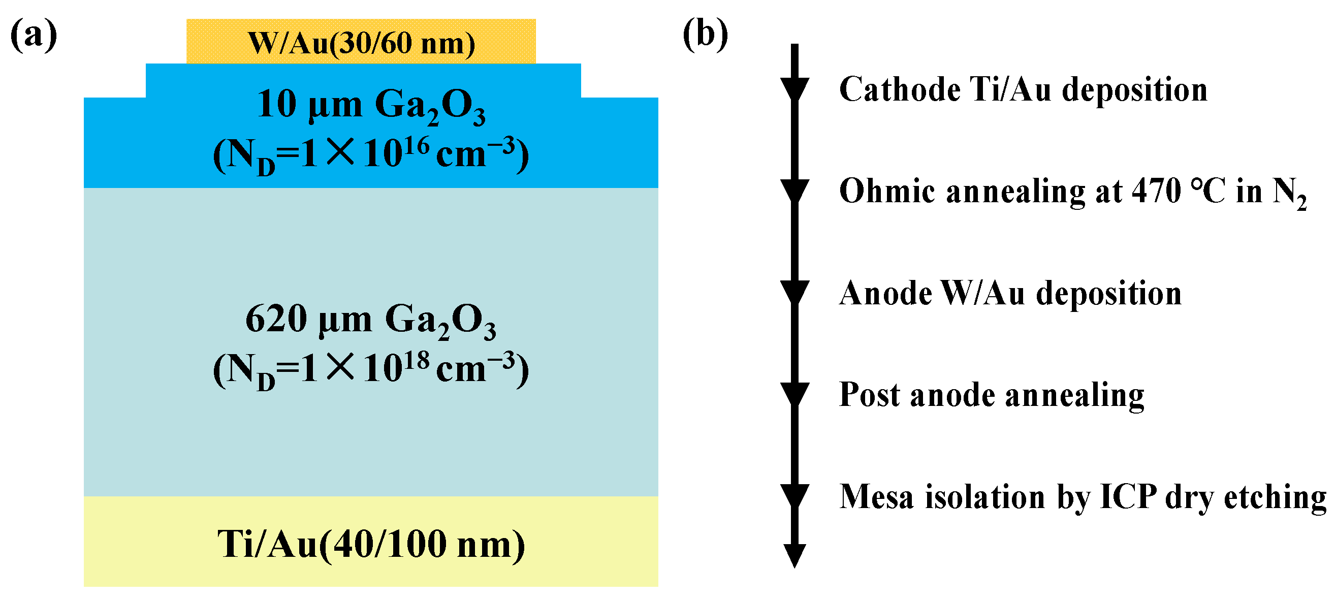
The schematic cross section structure of the fabricated Ga2O3 SBDs and the fabrication process are shown in Figure 1a and b, respectively. The substrate material was Sn-doped (n = 1 × 1018 cm−3) β-Ga2O3 single crystal substrates grown by the edge-defined film-fed growth method, then a 10-μm Si-doped (n = 1 × 1016 cm−3) epitaxial layer is grown by halide vapor phase epitaxy on top of β-Ga2O3 substrates. Prior to device fabrication, the wafer was cleaned with piranha solution and then soaked in dilute buffered oxide etch for 10 min to remove the surface residual contaminants. The full-area back cathode metal Ti/Au (40/100 nm) was deposited by electron-beam evaporation, followed by rapid annealing process at 470 °C in N2 for 60 s to form ohmic contacts. Then, the Schottky contacts were formed by the deposition of W/Au (30/60 nm), and 450 °C post-anode annealing for 2 min was performed in N2. Lastly, the mesa isolation was formed by inductively coupled plasma (ICP) dry etching with 1 μm depth. The C-V characteristics, the I-V measurement at varied temperatures ranging from 300 K to 450 K, and the reverse BV characteristics of the W/Au-Ga2O3 SBDs were taken with the Keysight B1505A semiconductor parameter analyzer, and the four-point probe testing method was used to reduce probe resistance.
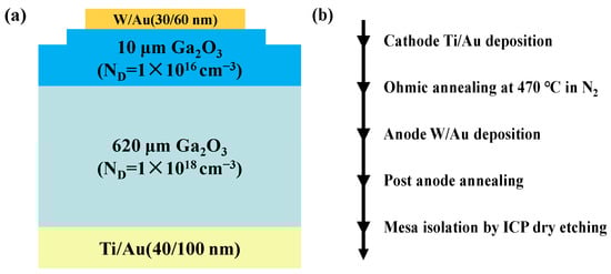
Figure 1.
(a) Schematic cross section structure of the fabricated W/Au Ga2O3 SBDs; (b) the fabrication process of the Ga2O3 SBDs.
3. Results and Discussion
Figure 2a shows the forward J-V characteristics of the W/Au Ga2O3 SBDs for the as-deposited sample and the sample with PAA. The barrier heights and ideality factors were extracted by fitting the linear regime of I-V curves using the thermionic emission model. After post-anode annealing, the barrier height increases from 0.85 eV to 0.88 eV and the ideality factor decreases from 1.21 to 1.14, respectively. In addition, as shown in Figure 2b, the breakdown voltage at the current density of 1 mA/cm2 increases by 56.25%, rising from 400 V to 625 V after the PAA treatment. On the surface of the Ga2O3 material, surface defects such as oxygen vacancies can lead to a large number of surface states, which can seriously affect the device characteristics [25]. The improvement of W/Au Ga2O3 diode characteristics after PAA treatment can be attributed to the reduction of surface defects, with further analysis shown below.
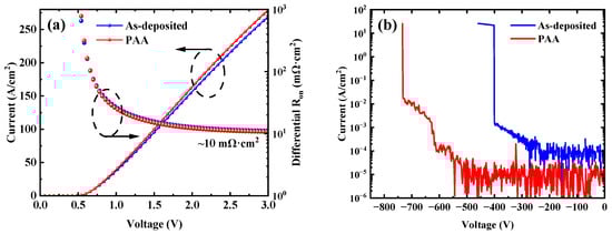
Figure 2.
(a) Forward J-V characteristics and (b) reverse BV characteristics of the W/Au Ga2O3 SBDs for the as-deposited sample and the sample with PAA.
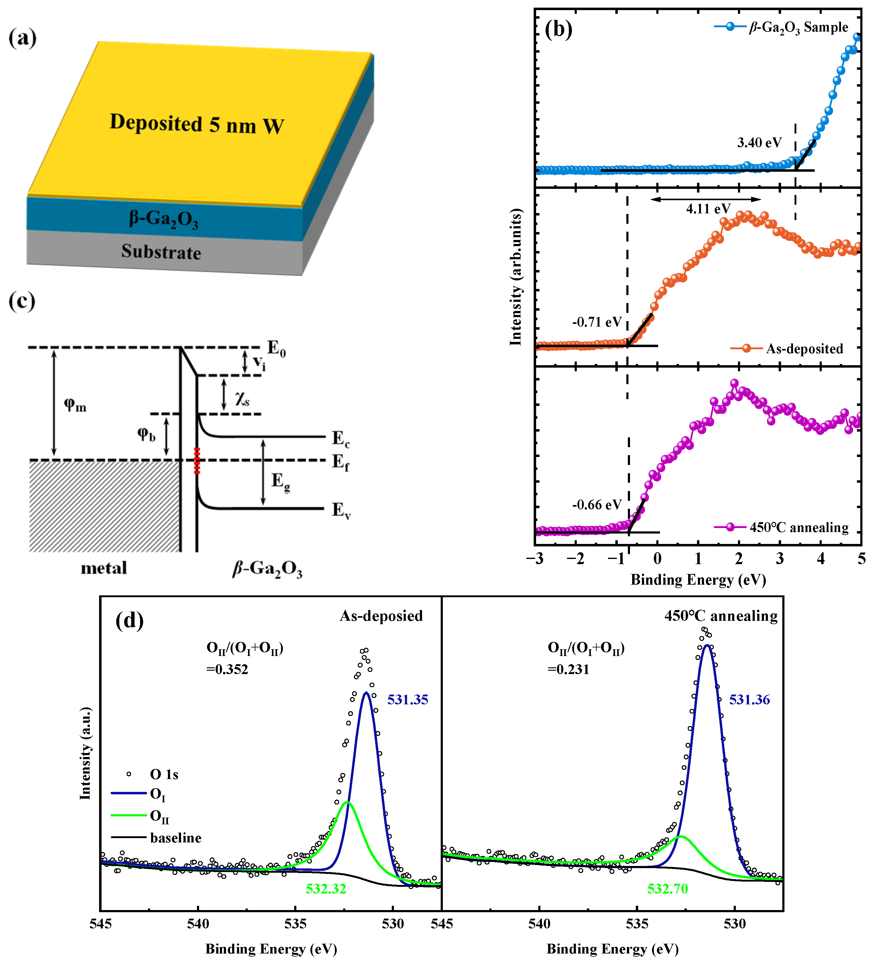
To investigate the improvement of W/Au Ga2O3 diode characteristics following PAA treatment, X-ray photoelectron spectroscopy (XPS) measurements were performed on the β-Ga2O3 samples. As shown in Figure 3a, a 5 nm thick W metal layer was deposited on the surface of the β-Ga2O3 sample. Prior to the XPS measurement, the W-deposited sample was etched with Ar+ plasma to enhance the accuracy of the results. Figure 3b presents the XPS valence band plots for the β-Ga2O3 sample, the as-deposited sample with the 5 nm W metal film, and the sample-deposited 5 nm W and with 450 °C annealing. According to Figure 3c, the barrier height (ϕb) of the metal contact with β-Ga2O3 can be expressed as ϕb = ϕm – χs – eVi, where the surface potential (Vi) is induced by the surface states located within the bandgap [26]. As illustrated in Figure 3b, the valence band maximum of the sample treated at 450 °C increases from −0.71 eV to −0.66 eV compared to the as-deposited sample. This difference indicates that the surface potential is reduced by about 0.05 eV after the 450 °C annealing, which is consistent with the increased barrier height extracted from the I-V characteristics. In addition, Figure 3d shows the O 1s core level spectra, which can be fitted into two peaks. The peaks around 531 eV (OI) and 533 eV (OII) are attributed to O2− ions and oxygen vacancies, respectively [27], and the proportion of OII represents the relative concentration of oxygen vacancies on the β-Ga2O3 surface. As shown in Figure 3d, the proportion of OII decreases from 35.2% to 23.1% after the 450 °C annealing treatment, indicating that the oxygen vacancies on the β-Ga2O3 surface are reduced. These oxygen vacancy defects act as surface states, whose reduction can lead to a decrease in the surface potential and an increase in the barrier height. At the same time, the oxygen vacancy defects and gallium–oxygen vacancy pairs are the origin of the donor-type defects and acceptor-type defects in the Ga2O3 material bandgap, respectively [28], where the reduction of oxygen vacancy defects on the β-Ga2O3 surface can also reduce the paths of electron assisted tunnelling through these defects [29], resulting in a decreased leakage current under reverse bias and an increased breakdown voltage.
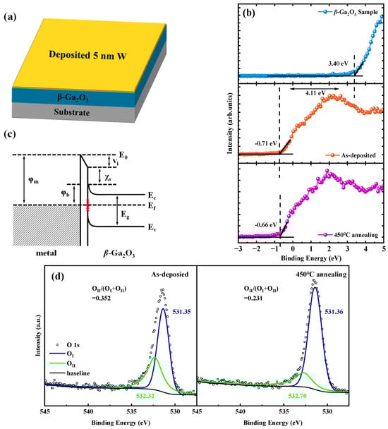
Figure 3.
(a) 5 nm thick W metal was deposited on the β-Ga2O3 sample surface; (b) XPS valence band plots for the β-Ga2O3 sample, as-deposited sample with 5 nm W metal film on Ga2O3, and the sample-deposited 5 nm W and annealed for 2 min at 450 °C in N2 atmosphere; (c) the barrier diagram of the metal in contact with β-Ga2O3; (d) the O 1s core level spectra for the sample-deposited 5 nm W and the sample-deposited 5 nm W with 450 °C annealing.
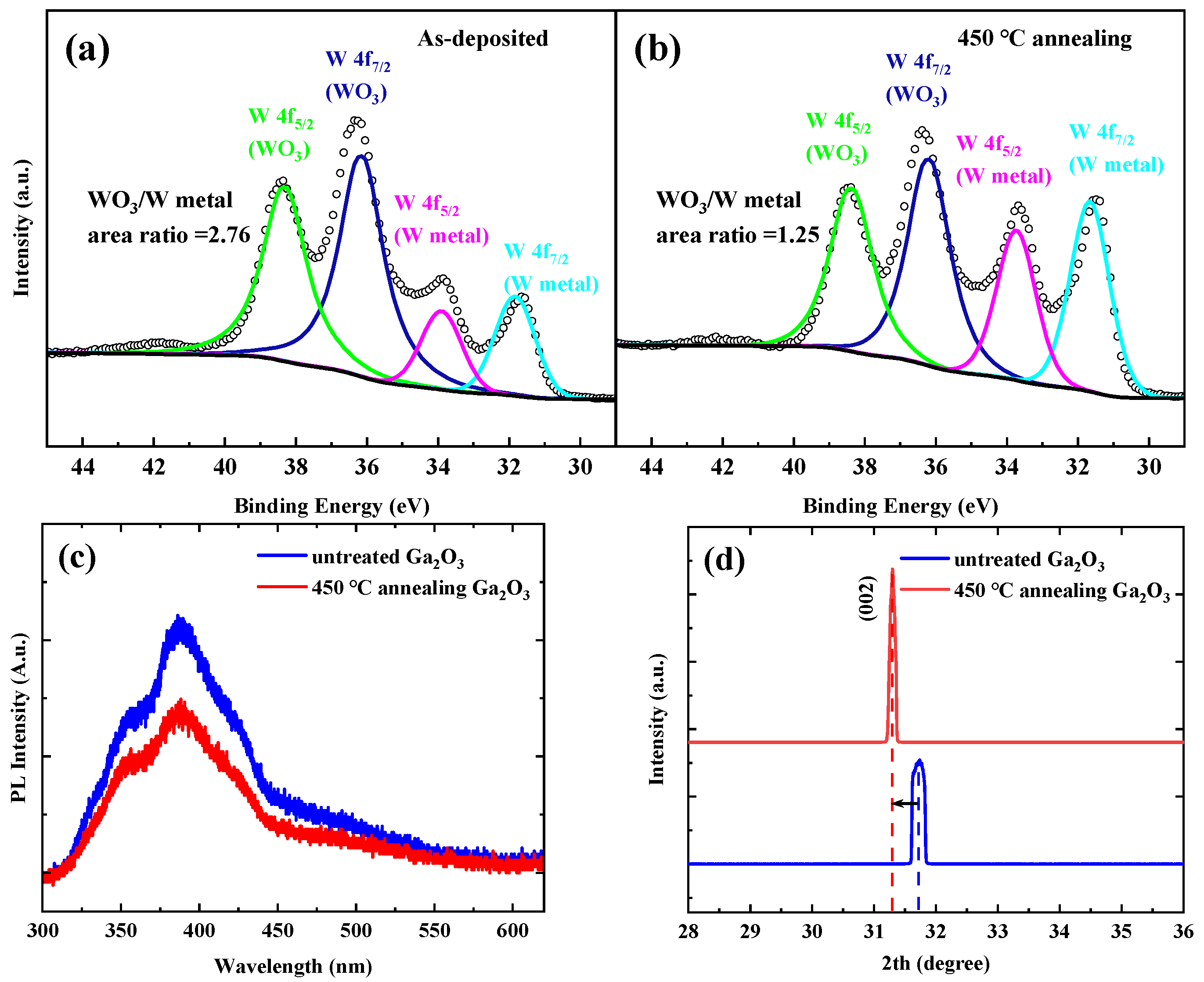
The reduction of oxygen vacancies on the β-Ga2O3 surface can be attributed to two aspects. On the one hand, the W metal has a low chemical affinity (i.e., lower oxide stability and no intermetallic compounds) with Ga2O3, so that WOx oxides are easily reduced to the W native metal during annealing [30]. Figure 4a and b show the W 4f spectra for the sample-deposited 5 nm W and the sample-deposited 5 nm W with 450 °C annealing. As shown in Figure 4a and Figure 4b, the peaks around 36.1 eV and 31.6 eV are attributed to WO3 and W metal, respectively. The W 4f core level spectra were deconvoluted using a doublet of two Gaussian peaks of equal width corresponding to the W 4f7/2 and W 4f5/2 spin-orbit components [31]. After annealing, the ratio of WO3 to W metal decreases from 2.76 to 1.25, indicating that WO3 oxides are partially reduced to the W native metal during annealing. Meanwhile, the excess oxygen atoms diffuse into the Ga2O3 material surface in the presence of pure nitrogen, thus reducing the surface oxygen vacancies. On the other hand, during the annealing process in nitrogen atmosphere, the oxygen atoms previously present in the Ga2O3 material interstitial positions have the probability to migrate to the correct position, which can also result in the reduction of oxygen vacancy and the improvement of Ga2O3 material crystal quality [32]. Figure 4c shows the PL spectra for the untreated Ga2O3 epitaxial material and the Ga2O3 epitaxial material with 450 °C annealing. As shown in Figure 4c, a significant emission peak at about 387 nm and a broad blue-green emission band are observed. In various Ga2O3 materials, the broad 350–620 nm emission band is common, and the origin can be ascribed to the emission recombination of electron and hole pairs between donor-type oxygen vacancy defects and acceptor-type gallium–oxygen vacancy pairs [28]. The PL emission intensity of the Ga2O3 epitaxial material decreases after annealing, demonstrating that the oxygen vacancies in the Ga2O3 material are reduced after annealing. Additionally, Figure 4d shows the XRD images for the untreated Ga2O3 epitaxial material and the Ga2O3 epitaxial material with 450 °C annealing in nitrogen atmosphere. The XRD results show that the intensity of the (002) diffraction peak (about 31.5°) is enhanced in the Ga2O3 epitaxial material with annealing. This indicates that the crystal quality of Ga2O3 epitaxial material is improved after annealing at 450 °C in N2 atmosphere, and the stress release leads to the location of the (002) peak shift [33]. These results are consistent with the previous conjectures.
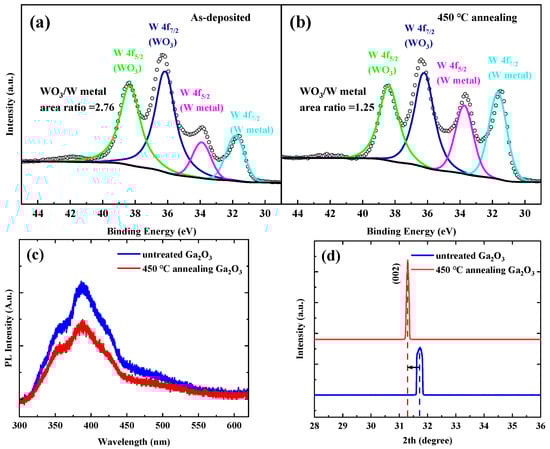
Figure 4.
The W 4f core level spectra for (a) the sample-deposited 5 nm W and (b) the sample-deposited 5 nm W with 450 °C annealing; (c) the PL spectra and (d) the 2th scan spectra for the untreated Ga2O3 epitaxial material and the Ga2O3 epitaxial material with 450 °C annealing.
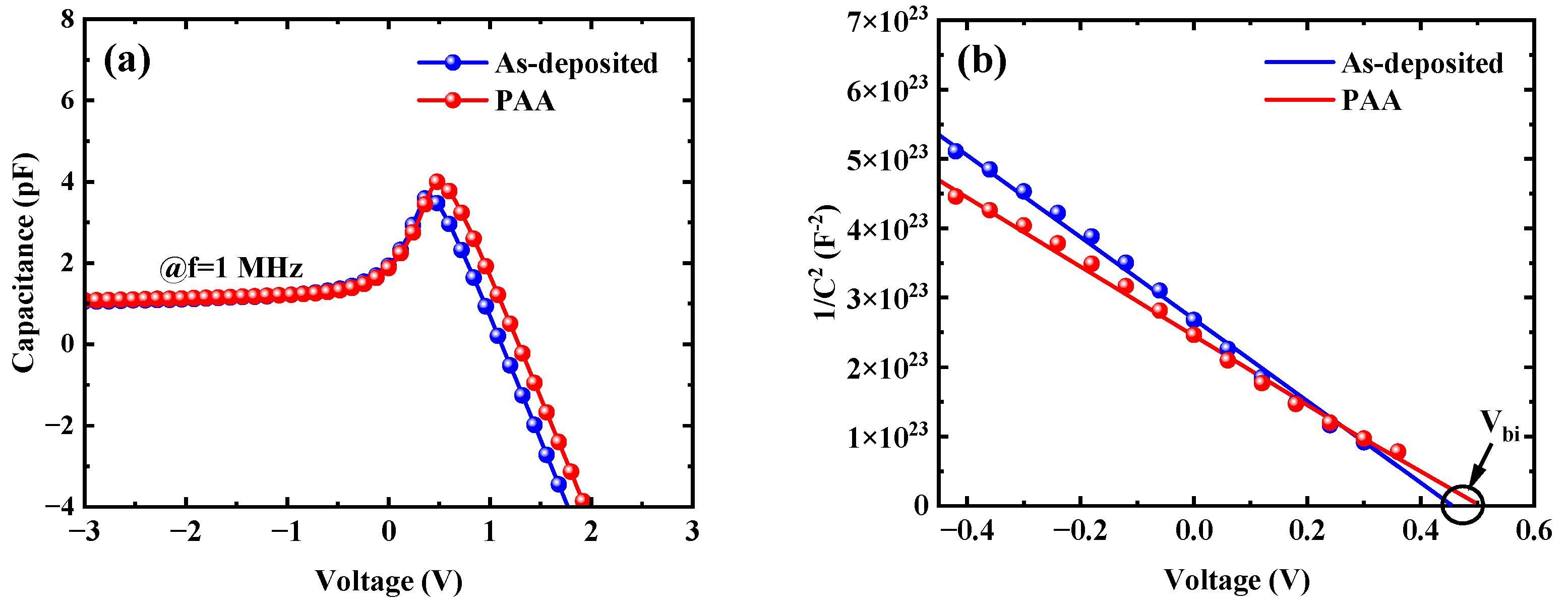
Figure 5a shows the C-V characteristics of the W/Au SBDs as a frequency of 1 MHz for the as-deposited sample and the sample with PAA, and it conforms to the typical behavior of vertical Schottky barrier diodes. As the anode voltage increases, majority carrier electrons accumulate gradually, leading to an increase of the capacitance [34]. Meanwhile, the capacitance 1/C2 versus applied voltage plots is shown in Figure 5b, and the relationship of the 1/C2-V is given by the following Equation [35]:
where C is the capacitance, A is the Schottky electrode area, εs is the dielectric constant of β-Ga2O3, ND is the effective carrier concentration, Фb is the effective barrier height, and Vn is the voltage corresponding to the difference between the conduction band edge (Ec) and the Fermi level (Ef) in the flat-band condition, which can be expressed as:
where Nc is the effective state density of the conduction band edge, which is given by:
where m* is the effective mass of electron, and h is the Planck constant. By combining Equations (1) and (2), the effective carrier concentration and barrier height can be calculated from the 1/C2-V plots as follows:
where Kc and Vbi are the slope of the 1/C2-V plots and the x-axis intercept of the 1/C2-V plots, respectively. As shown in Figure 5b, the calculated effective carrier concentrations are approximately 1.2 × 1015 cm−3, and the Фb,0 values obtained from C-V measurements are 0.72 eV for the as-deposited sample and 0.76 eV for the sample with PAA, where the calculated barrier heights are consistent with the results reported in the literature [36].
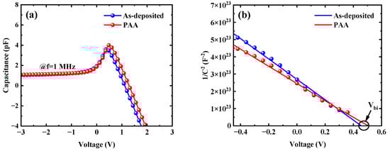
Figure 5.
(a) C-V characteristics and (b) 1/C2 versus voltage V plots for the as-deposited sample and the sample with 450 °C PAA.
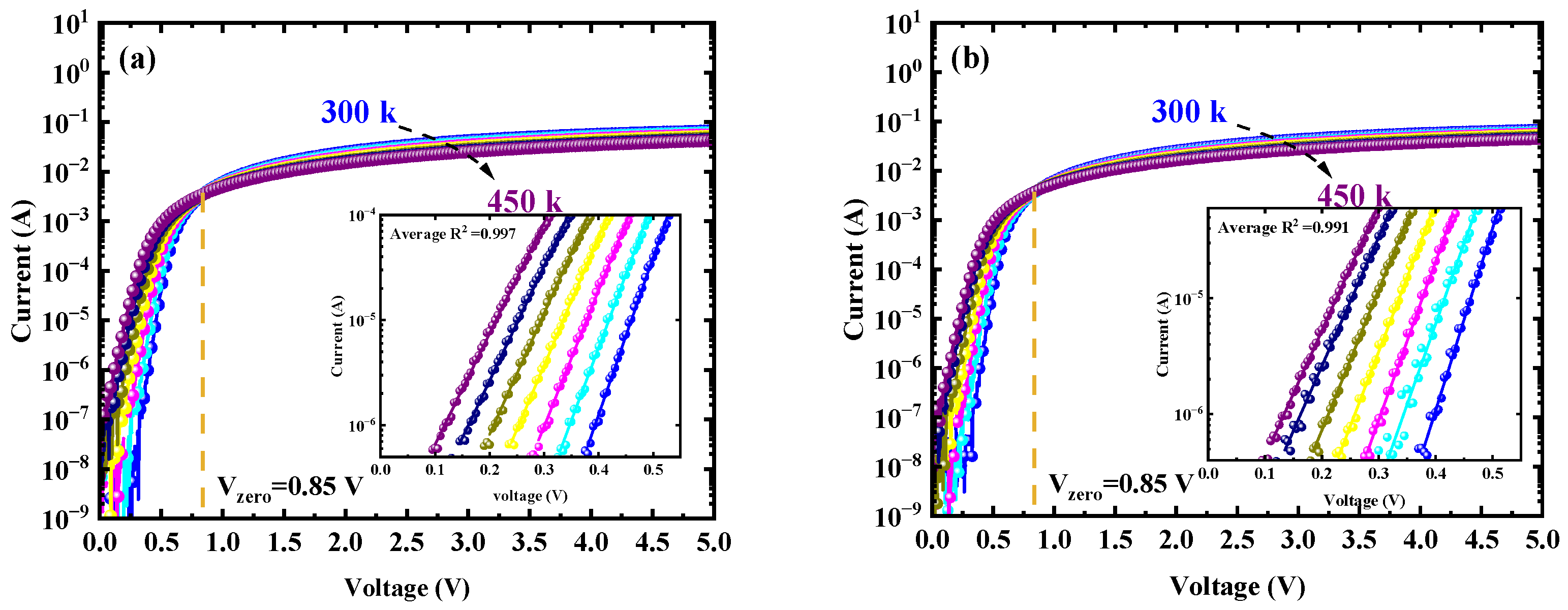
In order to investigate the barrier inhomogeneity of the W/Au Ga2O3 SBDs, the I-V characteristics of the Schottky diodes at varied temperatures ranging from 300 K to 450 K, as shown in Figure 6, were analyzed. A zero-crossing voltage Vzero was observed at 0.85 V in the as-deposited sample and the sample with PAA, which may be due to two different conduction mechanisms in the temperature dependence of the I-V characteristics [37]. When the forward voltage is below 0.85 V, electron thermionic emission is dominated between the W/Au metal and Ga2O3 contacts, with more electrons acquiring sufficient energy to overcome the Schottky barrier as the temperature rises, leading to an increase in current. Conversely, when the voltage exceeds 0.85 V, electron transport occurs within the drift layer, whereas the current is governed by the mobility of electrons in the drift layer. In this region, as the temperature rises, electron mobility decreases, resulting in a reduction in current.
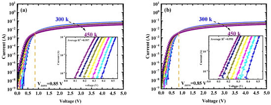
Figure 6.
The I-V characteristics of the W/Au Ga2O3 Schottky diodes at varied temperatures ranging from 300 K (blue) to 450 K (purple). (a) The as-deposited sample; (b) the sample with 450 °C PAA, and the inset is the linear region of the curves where a linear fit to the data is applied.
Based on the TE theory, the I-V characteristics are expressed by the following relationships [22,38]:
and
where A is the area of the Schottky contact, A** is the Richardson constant, with a theoretical value of 41.1 A/cm2K2 for β-Ga2O3, (calculated using m* = 0.34m0 from first-principles calculations), while k, q, T, and Is are the Boltzmann constant, electron charge, absolute temperature, and saturation current density, respectively. The Schottky barrier height qФb is the V-dependent Schottky barrier height and can be expressed as Фb = Фb,0 + βV, where β is the positive constant. Substituting this into Equation (6), the current can be rewritten as:
where η = 1/1 – β, and η is the ideality factor. When V > 3kq/T, Equation (8) simplifies to:
According to Equation (9), the saturation current density Is and the ideality factor η can be extracted from the slope and y-intercept y-intercept and slope of the ln(I)-V plots, respectively. In addition, the barrier height Фb was calculated from Equation (7). As shown in the inset of Figure 6, the barrier height was extracted by selecting a segment of the semi-logarithmic plot (approximately 0.1–0.5 V) within the linear region for linear fitting, from which the slope of the fitted Equation was determined. The obtained average goodness-of-fit metric R2 is very close to 1. Figure 7a shows the barrier height and ideality factor for the as-deposited sample and the sample with PAA as they were extracted at temperatures ranging from 300 K to 450 K. As the temperature increases, the barrier height increases and the ideality decreases, which is attributed to barrier inhomogeneities at the W/Au and Ga2O3 interface. The barrier inhomogeneities exhibited a strong temperature dependence process. At room temperature, carriers primarily cross regions with low barrier heights, often associated with defects at the W/Ga2O3 contact surface, resulting in a large ideality factor. However, as the temperature increased, the carriers gained sufficient energy to cross the higher barrier heights, leading to a smaller ideality factor. Furthermore, conventional Richardson’s plots ln(Is/T2) as a function of 1/kT were plotted for temperatures 300–450 K in Figure 7b. The barrier height qФb,0 and the Richardson constant A** were extracted from the slope and intercept of the linear fit, respectively. For the as-deposited sample, the calculated qФb,0 and A** are 0.69 eV and 0.082 A/cm2K2 respectively, while for the PAA-treated sample, these values are 0.76 eV and 0.481 A/cm2K2. The obtained Richardson constants are several orders of magnitude lower than the theoretical value of A** for β-Ga2O3. This discrepancy arises because the conventional Richardson plot assumes that the barrier height and ideality factor are temperature-independent, which is not valid in the presence of barrier inhomogeneities [25].
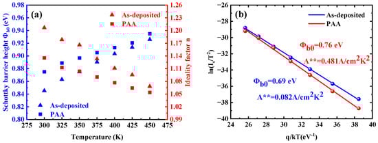
Figure 7.
(a) Extracted barrier height and ideality factor in W/Au Ga2O3 SBDs at temperatures 300–450 K and (b) the conventional Richardson’s plot ln(Is/T2) versus q/kT for the as-deposited sample and the sample with 450 °C PAA.
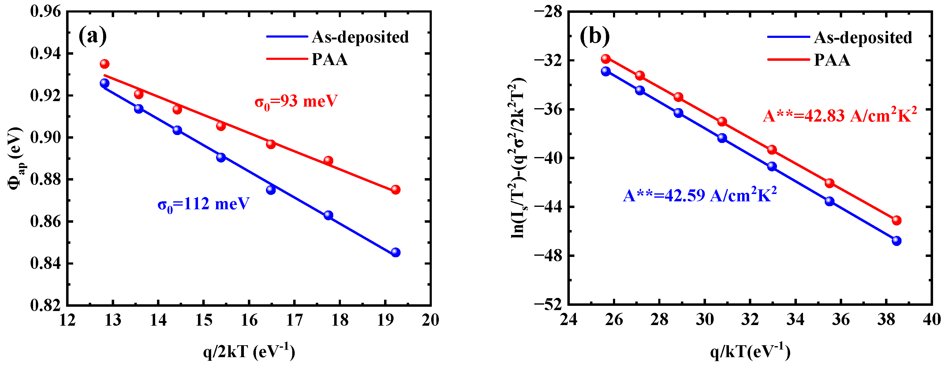
Thus, to explain the previously observed temperature dependence of barrier heights and ideality factors and the abnormal Richardson constants, barrier inhomogeneity was incorporated into the TE model in combination with a Gaussian distribution function for the barrier height, as expressed by the following Equation [39,40,41]:
where Фap is the apparent barrier height, Фb0 and σ0 are the mean barrier height and standard deviation, respectively. Figure 8a shows the Фap versus q/2kT plot, and the σ0 was determined with the slope of the fit line. The obtained σ0 values are 112 meV for the as-deposited sample and 92 meV for the sample with PAA. This reduction in σ0 after post-anode annealing is attributed to the reduction of oxygen vacancies, which serve as low-barrier height patches on the W/Ga2O3 contact surface, thereby decreasing fluctuations in the barrier height. Furthermore, a modified Richardson plot was derived using the following Equation:
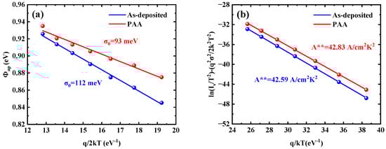
Figure 8.
(a) The Φap versus q/2kT plot and (b) the modified Richardson plot with the as-deposited sample and the sample with 450 °C PAA.
According to Equation (11), the modified Richardson plots are shown in Figure 8b. The modified Richardson constants were determined from the y-axis intercepts of the linear fits to the plots, yielding values of 42.59 A/cm2K2 for the as-deposited sample and 42.83 A/cm2K2 for the sample with PAA treatment. These values are close to the theoretical Richardson constant of 41.1 A/cm2K2. This result indicates that the barrier height of the W/Au-Ga2O3 Schottky contacts follows Gaussian distribution for both the as-deposited sample and the sample with PAA.
4. Conclusions
In conclusion, the electrical characteristics of β-Ga2O3 Schottky barrier diodes using W/Au as the Schottky metal were studied. Due to 450 °C post-anode annealing, the oxygen vacancy defects on the β-Ga2O3 surface were reduced, resulting in a decrease in the surface potential. The increase in barrier height and the reduction in leakage paths improved the characteristics of the W/Au-Ga2O3 SBDs, whereas the breakdown voltage increased by 56.25%, rising from 400 V to 625 V after PAA treatment. Additionally, the temperature dependence of barrier heights and ideality factors was observed over a temperature range of 300 K to 450 K, attributed to barrier inhomogeneity. The thermionic emission model combined with a Gaussian distribution of barrier heights was used to explain this temperature dependence. Post-annealing was found to reduce barrier height fluctuations from 112 meV to 92 meV. As evidenced by the modified Richardson constants of 42.59 A/cm2K2 for the as-deposited sample and 42.83 A/cm2K2 for the PAA-treated sample, both of which are very close to the theoretical Richardson constant for β-Ga2O3. These results demonstrate that the barrier inhomogeneity of W/Au-Ga2O3 SBDs can be effectively described using the TE model with a Gaussian distribution of barrier heights.
Author Contributions
Conceptualization, L.X. and T.Z.; methodology, L.X. and T.Z.; validation, T.Z., S.X. and J.Z.; formal analysis, L.X.; investigation, L.X.; resources, Y.H.; data curation, L.X.; writing—original draft preparation, L.X.; writing—review and editing, L.X., T.Z., S.X., H.S., H.T., Y.G. and X.L.; supervision, J.Z. and Y.H.; project administration, J.Z. and Y.H.; funding acquisition, T.Z., S.X., J.Z. and H.T. All authors have read and agreed to the published version of the manuscript.
Funding
This work was supported by the National Science Fund for Distinguished Young Scholars under Grant 61925404, National Key R & D Program of China under Grant 2022YFB3604400, National Natural Science Foundation of China under Grant 62104185, Grant 62074120, and Grant 62404167, Postdoctoral Fellowship Program of CPSF under Grant GZC20241306, and Natural Science Basic Research Program of Shaanxi Province under Grant 2023-JC-JQ-56.
Data Availability Statement
The original contributions presented in the study are included in the article, further inquiries can be directed to the corresponding author.
Conflicts of Interest
The authors declare no conflicts of interest.
References
- Cassabois, G.; Valvin, P.; Gil, B. Hexagonal boron nitride is an indirect bandgap semiconductor. Nat. Photonics 2016, 10, 262–266. [Google Scholar]
- Hickman, A.L.; Chaudhuri, R.; Bader, S.J.; Nomoto, K.; Li, L.; Hwang, J.C.M.; Grace Xing, H.; Jena, D. Next generation electronics on the ultrawide-bandgap aluminum nitride platform. Semicond. Sci. Technol. 2021, 36, 044001. [Google Scholar]
- Xie, L.; Xu, S.; Zhang, T.; Tao, H.; Su, H.; Gao, Y.; Liu, X.; Zhang, Y.; Zhang, J.; Hao, Y. Improved crystal quality of β-Ga2O3 on sapphire (0001) substrates by induced-nucleation technique and enhancement of Ga2O3 UV photodetectors performance. J. Alloys Compd. 2025, 1016, 178924. [Google Scholar]
- Sasama, Y.; Kageura, T.; Imura, M.; Watanabe, K.; Taniguchi, T.; Uchihashi, T.; Takahide, Y. High-mobility p-channel wide-bandgap transistors based on hydrogen-terminated diamond/hexagonal boron nitride heterostructures. Nat. Electron. 2022, 5, 37–44. [Google Scholar]
- Butenko, P.N.; Boiko, M.E.; Guzilova, L.I.; Krymov, V.M.; Shapenkov, S.V.; Sharkov, M.D.; Verbitskii, V.N.; Zarichny, A.A.; Nikolaev, V.I. Enhancing the perfection of bulk (100) β-Ga2O3 crystals grown by Czochralski method. J. Cryst. Growth 2024, 630, 127597. [Google Scholar]
- Sheoran, H.; Kumar, V.; Singh, R. A Comprehensive Review on Recent Developments in Ohmic and Schottky Contacts on Ga2O3 for Device Applications. ACS Appl. Electron. Mater. 2022, 4, 2589–2628. [Google Scholar]
- Ahmed, S.S.; Islam, A.E.; Dryden, D.M.; Liddy, K.J.; Hendricks, N.S.; Moser, N.A.; Chabak, K.D.; Green, A.J. Theoretical Power Figure-of-Merit in β-Ga2O3 Lateral Power Transistors Determined Using Physics-Based TCAD Simulation. IEEE Trans. Electron Devices 2024, 71, 5305–5312. [Google Scholar]
- Zhang, J.; Li, X.; Zhu, R.; Wang, K.; Zhang, B.; Zhang, C. Low loss and low EMI noise trench IGBT with shallow emitter trench controlled p-type dummy region. Chin. J. Electron. 2024, 33, 326–335. [Google Scholar]
- Liu, A.-C.; Hsieh, C.-H.; Langpoklakpam, C.; Singh, K.J.; Lee, W.-C.; Hsiao, Y.-K.; Horng, R.-H.; Kuo, H.-C.; Tu, C.-C. State-of-the-Art β-Ga2O3 Field-Effect Transistors for Power Electronics. ACS Omega 2022, 7, 36070–36091. [Google Scholar]
- Li, X.; Jiang, W.; Wang, Y.; Zhang, H.; Peng, C.; Zhang, X.; Liang, X.; Fu, W.; Zhang, Z.; Lei, Z.; et al. Single-event burnout in β-Ga2O3 Schottky barrier diode induced by high-energy proton. Appl. Phys. Lett. 2024, 125, 092101. [Google Scholar]
- Green, A.J.; Speck, J.; Xing, G.; Moens, P.; Allerstam, F.; Gumaelius, K.; Neyer, T.; Arias-Purdue, A.; Mehrotra, V.; Kuramata, A.; et al. β-Gallium oxide power electronics. APL Mater. 2022, 10, 029201. [Google Scholar] [CrossRef]
- Green, A.J.; Chabak, K.D.; Baldini, M.; Moser, N.; Gilbert, R.; Fitch, R.C.; Wagner, G.; Galazka, Z.; Mccandless, J.; Crespo, A.; et al. β-Ga2O3 MOSFETs for Radio Frequency Operation. IEEE Electron Device Lett. 2017, 38, 790–793. [Google Scholar] [CrossRef]
- Wong, M.H. A landscape of β-Ga2O3 Schottky power diodes. J. Semicond. 2023, 44, 091605. [Google Scholar] [CrossRef]
- Gammon, P.M.; Pérez-Tomás, A.; Shah, V.A.; Vavasour, O.; Donchev, E.; Pang, J.S.; Myronov, M.; Fisher, C.A.; Jennings, M.R.; Leadley, D.R.; et al. Modelling the inhomogeneous SiC Schottky interface. J. Appl. Phys. 2013, 114, 223704. [Google Scholar] [CrossRef]
- Splith, D.; Müller, S.; Schmidt, F.; von Wenckstern, H.; van Rensburg, J.J.; Meyer, W.E.; Grundmann, M. Determination of the mean and the homogeneous barrier height of Cu Schottky contacts on heteroepitaxial β-Ga2O3 thin films grown by pulsed laser deposition. Phys. Status Solidi A 2014, 211, 40–47. [Google Scholar] [CrossRef]
- Greco, G.; Giannazzo, F.; Fiorenza, P.; Di Franco, S.; Alberti, A.; Iucolano, F.; Cora, I.; Pecz, B.; Roccaforte, F. Barrier Inhomogeneity of Ni Schottky Contacts to Bulk GaN. Phys. Status Solidi A 2018, 215, 1700613. [Google Scholar] [CrossRef]
- Lee, K.Y.; Huang, Y.H. An Investigation on Barrier Inhomogeneities of 4H-SiC Schottky Barrier Diodes Induced by Surface Morphology and Traps. IEEE Trans. Electron Devices 2012, 59, 694–699. [Google Scholar] [CrossRef]
- Yadav, M.K.; Mondal, A.; Sharma, S.K.; Bag, A. Unveiling Thermal Effects on Sn-Doped β-Ga2O3 Schottky Barrier Diodes on Sapphire for High-Temperature Power Electronics. IEEE Trans. Electron Devices 2024, 71, 1529–1534. [Google Scholar] [CrossRef]
- Hou, C.; Gazoni, R.M.; Reeves, R.J.; Allen, M.W. Oxidized Metal Schottky Contacts on (010) β-Ga2O3. IEEE Electron Device Lett. 2019, 40, 337–340. [Google Scholar] [CrossRef]
- Taşçıoğlu, İ.; Aydemir, U.; Altındal, Ş. The explanation of barrier height inhomogeneities in Au/n-Si Schottky barrier diodes with organic thin interfacial layer. J. Appl. Phys. 2010, 108, 064506. [Google Scholar] [CrossRef]
- Triendl, F.; Pfusterschmied, G.; Pobegen, G.; Konrath, J.P.; Schmid, U. Theoretical and experimental investigations of barrier height inhomogeneities in poly-Si/4H-SiC heterojunction diodes. Semicond. Sci. Technol. 2020, 35, 115011. [Google Scholar]
- Reddy, P.R.S.; Janardhanam, V.; Shim, K.-H.; Reddy, V.R.; Lee, S.-N.; Park, S.-J.; Choi, C.-J. Temperature-dependent Schottky barrier parameters of Ni/Au on n-type (001) β-Ga2O3 Schottky barrier diode. Vacuum 2020, 171, 109012. [Google Scholar]
- Higashiwaki, M.; Konishi, K.; Sasaki, K.; Goto, K.; Nomura, K.; Thieu, Q.T.; Togashi, R.; Murakami, H.; Kumagai, Y.; Monemar, B.; et al. Temperature-dependent capacitance–voltage and current–voltage characteristics of Pt/Ga2O3 (001) Schottky barrier diodes fabricated on n-–Ga2O3 drift layers grown by halide vapor phase epitaxy. Appl. Phys. Lett. 2016, 108, 133503. [Google Scholar]
- Hou, C.; Gazoni, R.M.; Reeves, R.J.; Allen, M.W. Dramatic Improvement in the Rectifying Properties of Pd Schottky Contacts on β-Ga2O3 During Their High-Temperature Operation. IEEE Trans. Electron Devices 2021, 68, 1791–1797. [Google Scholar]
- Iucolano, F.; Roccaforte, F.; Giannazzo, F.; Raineri, V. Barrier inhomogeneity and electrical properties of Pt/GaN Schottky contacts. J. Appl. Phys. 2007, 102, 113701. [Google Scholar]
- Garg, M.; Naik, T.R.; Pathak, C.S.; Nagarajan, S.; Rao, V.R.; Singh, R. Significant improvement in the electrical characteristics of Schottky barrier diodes on molecularly modified Gallium Nitride surfaces. Appl. Phys. Lett. 2018, 112, 163502. [Google Scholar]
- Qian, L.-X.; Wu, Z.-H.; Zhang, Y.-Y.; Lai, P.T.; Liu, X.-Z.; Li, Y.-R. Ultrahigh-Responsivity, Rapid-Recovery, Solar-Blind Photodetector Based on Highly Nonstoichiometric Amorphous Gallium Oxide. ACS Photonics 2017, 4, 2203–2211. [Google Scholar]
- Mi, W.; Ma, J.; Luan, C.; Xiao, H. Structural and optical properties of β-Ga2O3 films deposited on MgAl2O4 (100) substrates by metal–organic chemical vapor deposition. J. Lumin. 2014, 146, 1–5. [Google Scholar]
- Polyakov, A.; Lee, I.-H.; Smirnov, N.; Shchemerov, I.; Vasilev, A.; Chernykh, A.; Pearton, S. Electric field dependence of major electron trap emission in bulk β-Ga2O3: Poole–Frenkel effect versus phonon-assisted tunneling. J. Phys. D Appl. Phys. 2020, 53, 304001. [Google Scholar]
- Yao, Y.; Davis, R.F.; Porter, L.M. Investigation of Different Metals as Ohmic Contacts to β-Ga2O3: Comparison and Analysis of Electrical Behavior, Morphology, and Other Physical Properties. J. Electron. Mater. 2017, 46, 2053–2060. [Google Scholar]
- Zhang, T.; Lee, C.-Y.; Gong, B.; Lim, S.; Wenham, S.; Hoex, B. In situ x-ray photoelectron emission analysis of the thermal stability of atomic layer deposited WOx as hole-selective contacts for Si solar cells. J. Vac. Sci. Technol. A 2018, 36, 031601. [Google Scholar]
- Chen, W.-J.; Ma, H.-P.; Gu, L.; Shen, Y.; Yang, R.-Y.; Zhang, J.; Yang, L.; Zhu, J.; Zhang, Q.-C. Influence of nitrogen annealing treatment on optical, microstructural, and chemical properties of Ga2O3 film grown by plasma-enhanced atomic layer deposition. J. Phys. Chem. C 2023, 127, 10688–10698. [Google Scholar]
- Gao, S.; Yang, X.; Cheng, J.; Guo, X.; Kang, R. Deformation and fracture behaviors of monocrystalline β-Ga2O3 characterized using indentation method and first-principles calculations. Mater. Charact. 2023, 200, 112920. [Google Scholar]
- Hong, Y.; Zheng, X.; He, Y.; Liu, K.; Zhang, H.; Wang, X.; Yuan, Z.; Zhang, F.; Wang, Y.; Ma, X.; et al. Enhancing performance of β-Ga2O3 diodes through a NixO/SiNx/Ga2O3 sandwich structure. J. Alloys Compd. 2024, 976, 173062. [Google Scholar]
- Wang, Z.; Gong, H.-H.; Yu, X.-X.; Ji, X.; Ren, F.-F.; Yang, Y.; Gu, S.; Zheng, Y.; Zhang, R.; Ye, J. Trap-mediated bipolar charge transport in NiO/Ga2O3 p+-n heterojunction power diodes. Sci. China Mater. 2023, 66, 1157–1164. [Google Scholar] [CrossRef]
- Xian, M.; Fares, C.; Ren, F.; Gila, B.P.; Chen, Y.-T.; Liao, Y.-T.; Tadjer, M.; Pearton, S.J. Effect of thermal annealing for W/β-Ga2O3 Schottky diodes up to 600 °C. J. Vac. Sci. Technol. B 2019, 37, 061201. [Google Scholar]
- Chen, J.; Bian, Z.; Liu, Z.; Zhu, D.; Duan, X.; Wu, Y.; Jia, Y.; Ning, J.; Zhang, J.; Hao, Y. Effects of thermal annealing on the electrical and structural properties of Mo/Au schottky contacts on n-GaN. J. Alloys Compd. 2021, 853, 156978. [Google Scholar]
- Tung, R.T. Electron transport at metal-semiconductor interfaces: General theory. Phys. Rev. B 1992, 45, 13509–13523. [Google Scholar]
- Subhash, C.; Jitendra, K. Simulation and analysis of the I-V characteristics of a Schottky diode containing barrier inhomogeneities. Semicond. Sci. Technol. 1997, 12, 899. [Google Scholar]
- Chand, S.; Kumar, J. Effects of barrier height distribution on the behavior of a Schottky diode. J. Appl. Phys. 1997, 82, 5005–5010. [Google Scholar]
- Pakma, O.; Serin, N.; Serin, T.; Altındal, Ş. The double Gaussian distribution of barrier heights in Al/TiO2/p-Si (metal-insulator-semiconductor) structures at low temperatures. J. Appl. Phys. 2008, 104, 014501. [Google Scholar] [CrossRef]


Disclaimer/Publisher’s Note: The statements, opinions and data contained in all publications are solely those of the individual author(s) and contributor(s) and not of MDPI and/or the editor(s). MDPI and/or the editor(s) disclaim responsibility for any injury to people or property resulting from any ideas, methods, instructions or products referred to in the content. |
© 2025 by the authors. Licensee MDPI, Basel, Switzerland. This article is an open access article distributed under the terms and conditions of the Creative Commons Attribution (CC BY) license (https://creativecommons.org/licenses/by/4.0/).