1. Introduction
Surface acoustic wave filters utilize acoustic waves that propagate on the surface of piezoelectric crystals to provide excellent frequency selectivity with a compact device size [
1,
2,
3]. As mobile communication technology advances, the fifth-generation has become the leading force in current and future wireless communications. As critical components in 5G systems, SAW filters are crucial for achieving high-speed data transmission, low loss, and wide bandwidths [
4,
5,
6,
7]. Their application in 5G systems enhances data transfer rates, reduces latency, and improves signal coverage, significantly optimizing system performance and communication quality. Traditional SAW devices typically use bulk piezoelectric single crystals such as LiNbO
3, quartz, and LiTaO
3, which, despite their lower acoustic velocities, ionic volatility at high temperatures, electromechanical coupling coefficient, and quality factors, are limited in high-frequency applications [
8,
9,
10]. Although ZnO and AlN thin films offer higher acoustic velocities, their lower electromechanical coupling coefficients make them primarily suitable for narrowband SAW devices [
11,
12].
To address these limitations, researchers have explored bonding piezoelectric single-crystal films with other materials to leverage their combined advantages and develop high-performance SAW devices. The selection of appropriate materials can result in high sound propagation speeds, high electromechanical coupling coefficients, and improved TCF characteristics. For instance, Hashimoto et al. investigated the acoustic wave propagation characteristics of Cu-Grating/Y-X LiNbO
3/SiO
2/Si substrates [
13]. Ikata et al. developed trapezoidal SAW filters for different frequencies and demonstrated the potential of this type of substrate structure in the development of ultra-wideband and low-loss RF SAW filters [
14]. Tao et al. studied the effects of various material thicknesses on the performance of SAW filters based on LiNbO
3/SiO
2/Si multi-layer structures and experimentally validated their theoretical results [
15]. Hus et al. designed wideband radio-frequency shear-horizontal surface acoustic wave resonators based on a LiNbO
3/SiO
2/Si functional substrates and demonstrated the feasibility of developing broadband acoustic RF devices for potential 5G wireless communications [
16]. Feng et al. examined a SAW filter based on IDT (Cu)/15° Y-X LiNbO
3/SiO
2/Si substrate structures and analyzed the impact of electrode parameters on the electromechanical coupling coefficient and the performance of the trapezoidal filter [
17]. Their results revealed excellent bandpass filter characteristics, a good frequency temperature coefficient, and strong power durability. Pan et al. explored the performance of a SAW resonator on a 42° Y-X LiTaO
3 multi-layer substrate, optimized the thickness of each layer in the 42° Y-X LiTaO
3/SiO
2 substrate, and studied the effects of device structure parameters on dispersion and slow-wave curves. Their experimental results were consistent with simulation results, indicating that optimizing the materials and thicknesses of multi-layer film structures can significantly enhance SAW device performance [
18].
This paper proposes a SAW resonator based on a 41° Y-X LiNbO3/SiO2/poly-Si/Si multi-layered structure. A comprehensive analysis of the proposed SAW resonator is conducted using analytical theory and finite element methods. First, the governing equations for the SAW propagating along the multi-layered structure are derived based on the constitutive relationships between the mechanical displacement and electric field in the piezoelectric film. Subsequently, finite element software COMSOL5.5 is utilized to investigate the effects of LiNbO3, SiO2, and Al electrodes on key performance parameters, such as the device admittance characteristics, phase velocity, and bandwidth, providing guidance for the comprehensive optimal design of SAW devices. Finally, based on the simulation results, the optimal substrate and electrode structures are determined. A SAW resonator is fabricated on a 41° Y-X LiNbO3/SiO2/poly-Si/Si multi-layered substrate and its application to a wideband SAW filter is explored.
3. Modeling and Simulation
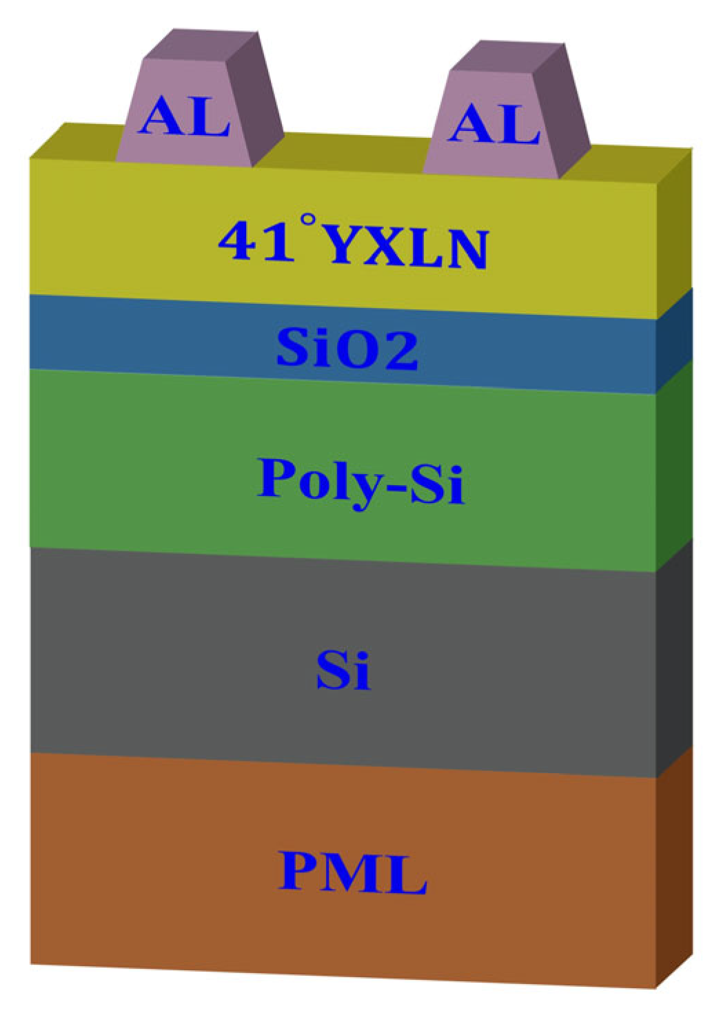
The high performance of multi-layer SAW devices is achieved by utilizing the advantages of various materials and multi-layer film structures to confine the acoustic wave energy to the material’s surface and enhance the quality factor. This paper comprehensively analyzes the effects of different material thicknesses on the performance of SAW resonators based on a 41° Y-X LiNiO
3 substrate. The SAW resonator structure is illustrated in
Figure 2 and includes a perfectly matched layer (PML), Si, poly-Si, SiO
2, 41° Y-X LiNiO
3, and an Al electrode. The SiO
2 serves as both a low acoustic impedance layer and a temperature compensation layer, the poly-Si acts as an electron trapping layer, and the high-resistivity Si serves as the supporting substrate.
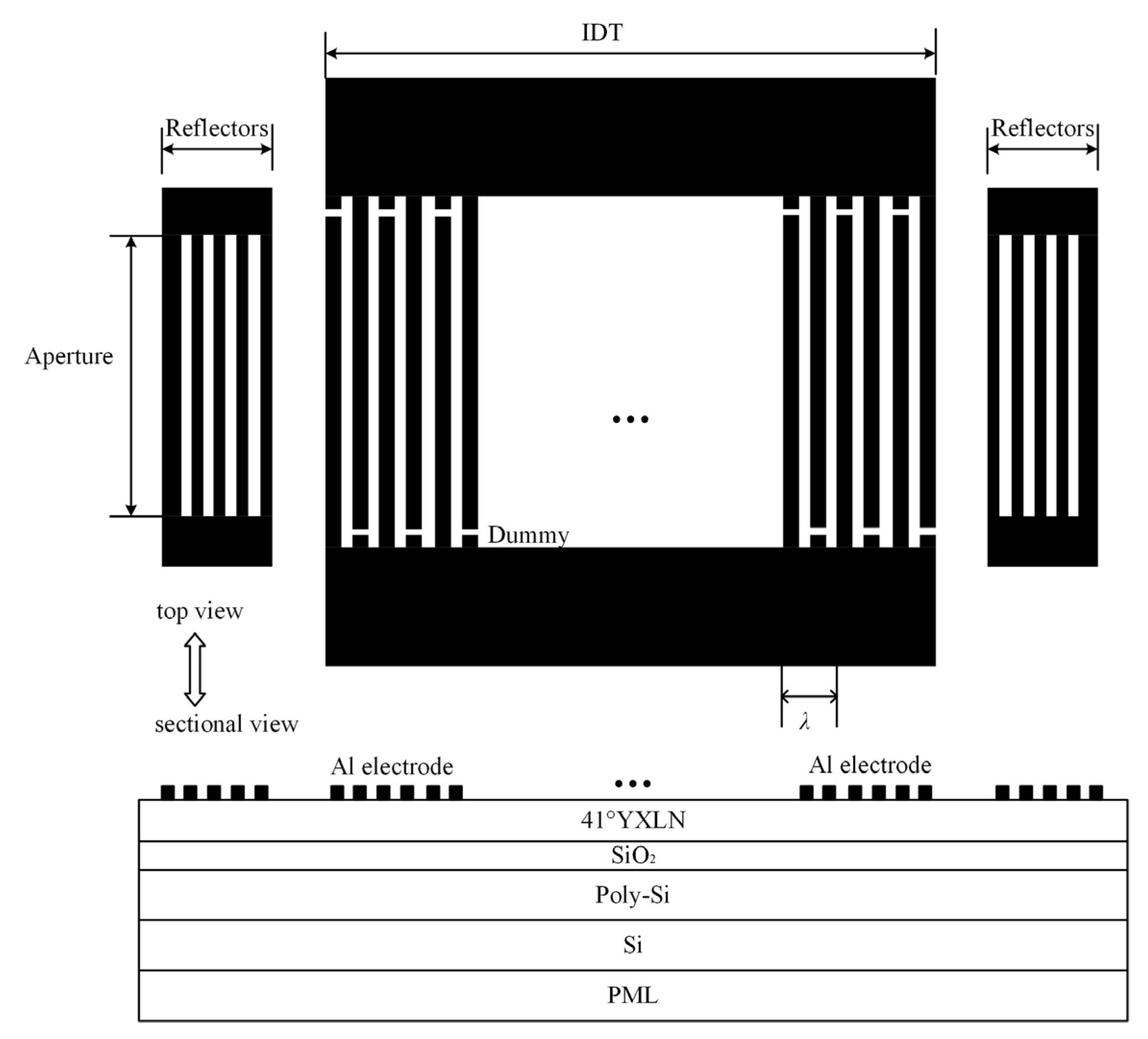
Figure 3 is the schematic diagram of the one-port SAW resonator on a 41° Y-X LiNbO
3/SiO
2/poly-Si/Si multi-layer film structure.
Assuming the SAW propagates along a designated direction in the multi-layer film structure, the full-scale 3D finite element model is simplified to a double-finger structure with a single-period size. A PML is also constructed at the bottom to absorb acoustic waves propagating into the substrate, eliminating interference from reflected signals. Periodic boundary conditions are applied on both sides of the model to extend it infinitely in the propagation direction. To ensure both simulation accuracy and speed, the mesh size in the area below the electrode is set to be smaller than in the other substrate areas. This is because the geometric shape of the Al electrodes in practical processing is trapezoidal, and the acoustic wave energy in the thickness direction decays rapidly, concentrating primarily on the surface of the piezoelectric film.
The COMSOL finite element software can simulate various physical fields, such as vibrations and electric fields [
21]. Thus, as shown in
Figure 2, an infinite-period model is used for frequency-domain simulation with the MUMPS solver to optimize the thicknesses of different layers for optimal device performance.
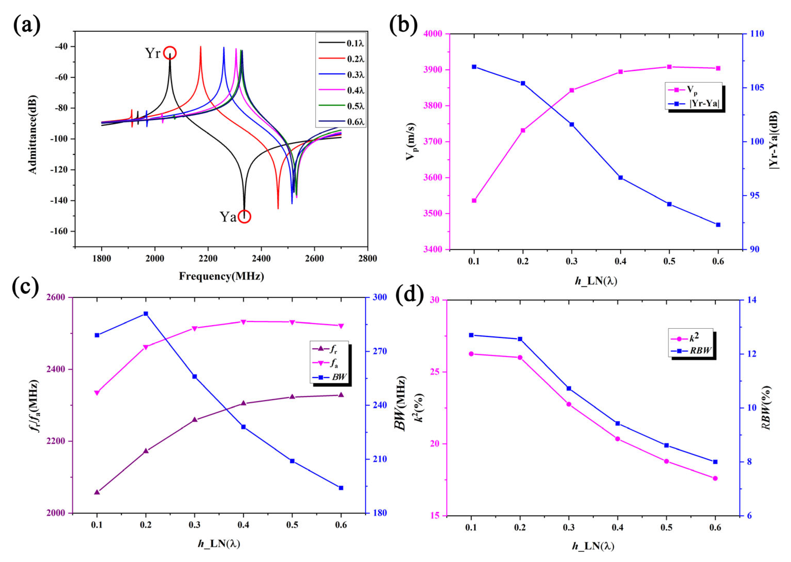
Figure 4 shows the frequency characteristics as a function of the LiNbO
3 thickness
h_LN. The IDT period is set to 1.61 μm, the IDT metalization ratio is 0.5, the Al electrode thickness
h_Al is 180 nm, the SiO
2 thickness
h_SiO
2 is 450 nm, and the poly-Si thickness is fixed at 1 μm. During the calculations, the thickness of the bottom Si substrate is set to 4.83 μm, and the PML thickness is set to 3.22 μm. The corresponding material parameters of the simulation are show in
Table 1.
Figure 4a compares the admittance curves of the SAW resonator for different LiNbO
3 thicknesses. Here, Y
r and Y
a are the peak value of the admittance curve. It is evident that the LiNbO
3 thickness significantly impacts the frequency characteristics of the SAW resonator, with the resonant frequency increasing as the LiNbO
3 thickness increases.
Figure 4a shows that spurious waves near the resonant frequency are effectively suppressed.
Figure 4b clearly illustrates the dependence of the phase velocity V
p and admittance difference |Y
r − Y
a| on the LiNbO
3 thickness. The phase velocity increases with the LiNbO
3 thickness, indicating dispersion effects for high-frequency SAWs, with high-speed waves appearing within the expected range. Conversely, the admittance difference decreases with increasing LiNbO
3 thickness, with a smaller admittance difference indicating a poorer out-of-band suppression capability.
Figure 4c shows the effects of the LiNbO
3 thickness on the resonant frequency
fr which is the frequency corresponding to Y
r, anti-resonant frequency
fa which is the frequency corresponding to Y
a, and bandwidth
BW. It is observed that
fr and
fa both increase with the LiNbO
3 thickness, while
BW initially increases and then decreases, reaching a maximum value when the LiNbO
3 thickness is 0.2 L.
Figure 4d shows that the electromechanical coupling coefficient
k2 and relative bandwidth
RBW values decrease non-linearly with increasing LN thickness. Here, V
p,
BW,
k2, and
RBW could be describe as:
With an increased LiNbO3 thickness, parameters such as the resonance frequency, phase velocity, admittance deviation, electromechanical coupling coefficient, and bandwidth change monotonically. This is because the energy of the SH wave is primarily concentrated on the material’s surface. As the piezoelectric film becomes thicker, its performance becomes similar to that of an SH wave on a 41° YX LiNbO3 structure.
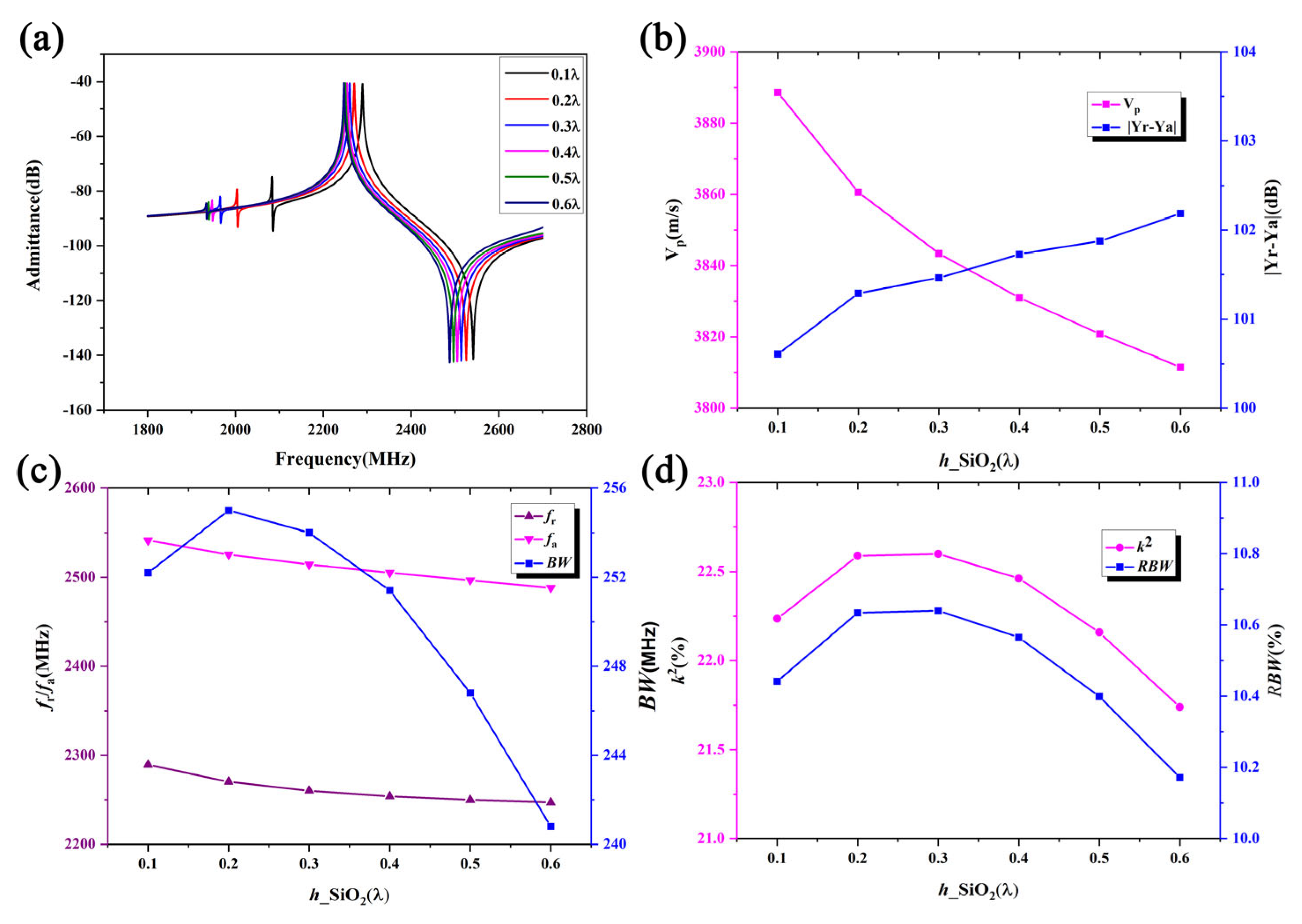
The effect of the SiO
2 layer, which provides temperature compensation, on the overall performance of the surface acoustic wave resonator is also noteworthy. To study this, the IDT period is also set to 1.61 μm, with the IDT metalization ratio is the same as above, an Al electrode thickness of 180 nm, a LiNbO
3 thickness of 490 nm, and the poly-Si thickness fixed at 1 μm.
Figure 5a compares the admittance curves of the SAW resonator with different SiO
2 thicknesses. It can be seen that the resonance frequency decreases monotonically with increasing SiO
2 thickness.
Figure 5b shows the relationship between the phase velocity and admittance deviation as a function of the SiO
2 thickness. It is clear that the phase velocity decreases with increasing SiO
2 thickness while the admittance deviation increases.
Figure 5c shows the effect of the SiO
2 thickness on the resonance frequency, anti-resonance frequency, and bandwidth. It can be observed that the resonance frequency and the anti-resonance frequency decrease slowly with increasing SiO
2 thickness, and the bandwidth first increases and then gradually decreases, reaching a maximum value when the SiO
2 thickness is 0.2 L.
Figure 5d shows the relationship between
k2 and relative bandwidth
RBW as a function of the SiO
2 thickness. Clearly, both the electromechanical coupling coefficient
k2 and
RBW values decrease non-linearly with increasing SiO
2 thickness, reaching a maximum value at SiO
2 thicknesses of approximately 0.2 λ to 0.3 λ.
Apart from LiNbO
3 and SiO
2, the thickness of the Al electrode also affects the SAW performance due to mass loading. Therefore, the effect of the Al electrode thickness is also investigated in this work. Specifically, the IDT period is set to 1.61 μm, with a metal duty cycle of 0.5, a LiNbO
3 thickness of 490 nm, a SiO
2 thickness of 420 nm, and a poly-Si thickness of 1 μm. The performance of the SAW resonator with different Al electrode thicknesses is calculated.
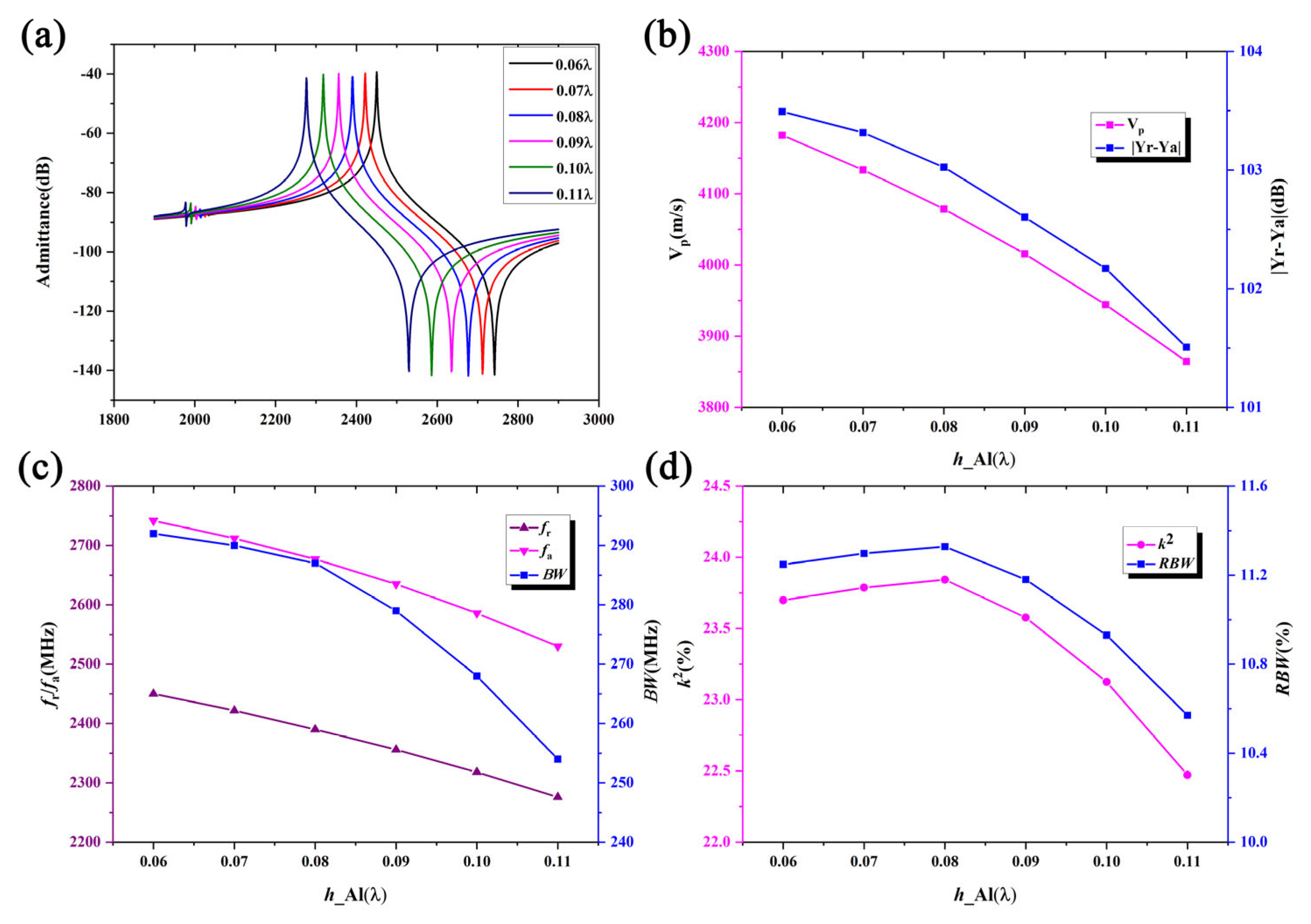
Figure 6 shows the change in the admittance curves with increasing Al thickness. It is clear that as the Al thickness increases, the mass loading of the Al electrode causes the resonance frequency to decrease gradually. Additionally, since different acoustic wave modes in the piezoelectric dielectric have different excitation efficiencies, it is necessary to select an appropriate Al electrode thickness to suppress spurious waves within the passband.
Figure 6 shows that as the Al electrode thickness varies, the phase velocity, resonance frequency,
k2, and
RBW values exhibit similar curves to those seen for a changing SiO
2 thickness. However, in contrast to the SiO
2 thickness variation curves, the admittance deviation and bandwidth decrease with increasing Al electrode thickness.
The above analysis shows that the LiNbO3 thickness significantly impacts the velocity, admittance deviation, and k2 values. Compared to the LiNbO3 thickness, the SiO2 thickness has a smaller effect on these parameters, and the Al electrode thickness primarily affects the velocity. Optimal resonator performance with high coupling of 24% operating frequency more than 2.2 GHz is achieved when configured with a LiNbO3 thickness of 490 nm, a SiO2 thickness of 420 nm, and an Al electrode thickness of 130 nm.
4. Design Verification of Resonator and Its Application to Filter
Based on the above simulation results, a multi-layer Al/41° Y-X LiNbO
3/SiO
2/poly-Si/Si structure SAW resonator was manufactured as shown in
Figure 3, with an Al electrode thickness of 130 nm, a LiNbO
3 thickness of 490 nm, a SiO
2 thickness of 420 nm, and a polysilicon thickness of 1300 nm. The resonator includes 251 IDTs and 5 finger reflector arrays, and its aperture is weighted using a cosine function in order to achieve lateral mode suppression.
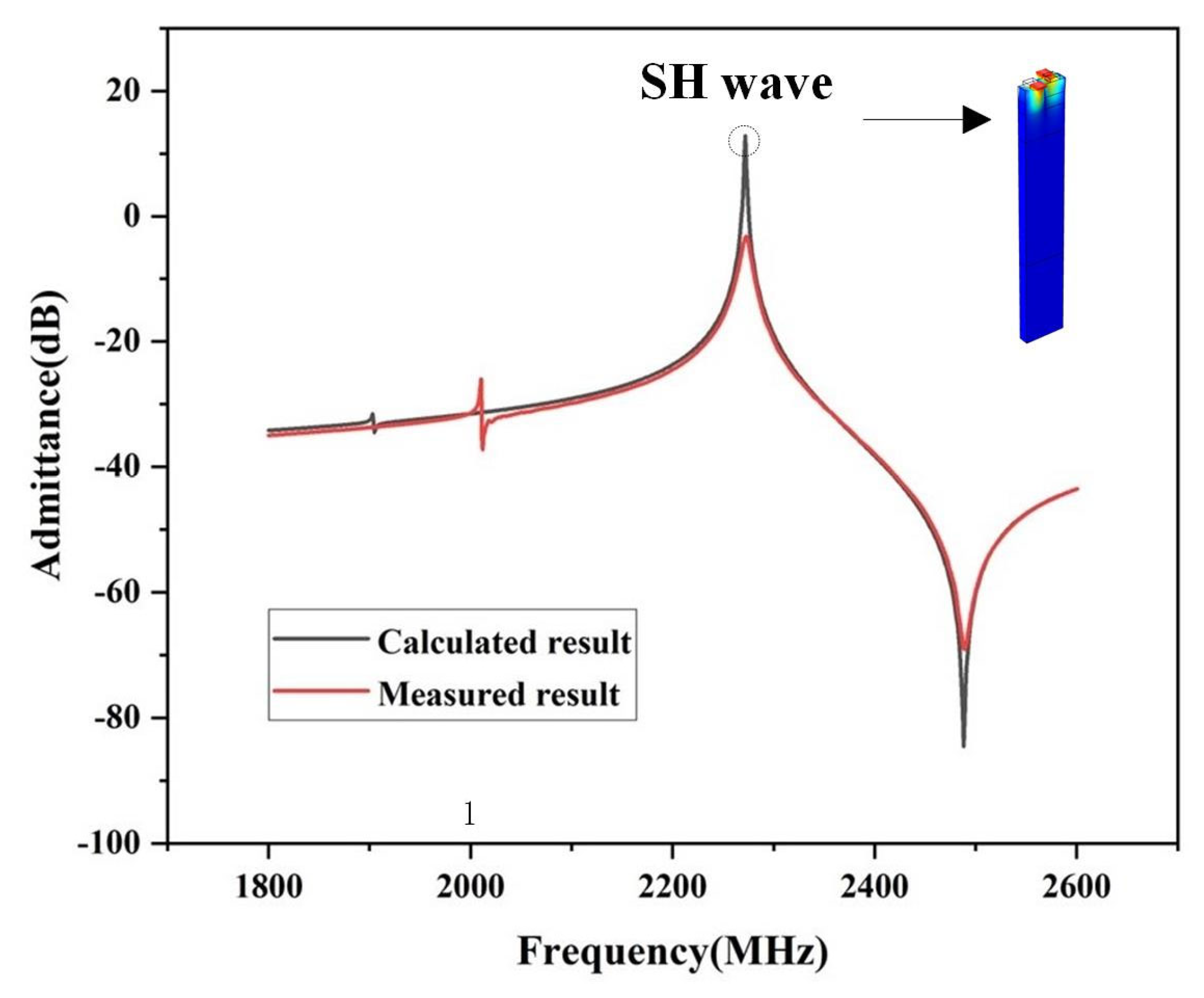
Figure 7 shows the measured and simulated admittance Y
11 curves of the SAW device. The displacement contour is also given in the Figure as an insert. As shown, a transverse polarization state can be observed, which is the so-called SH wave acoustic mode. Analysis of
Figure 7 indicates that the bandwidth of the measured results is consistent with the simulated bandwidth, while there is a certain discrepancy between the measured and simulated
k2 values. This discrepancy arises from several factors: (1) the simulation calculations use ideal parameters, while actual materials may differ; (2) there may be discrepancies between the actual and simulated material thicknesses due to process errors and possible damage to the material lattice during production; and (3) there are electrical parasitic effects such as insertion loss.
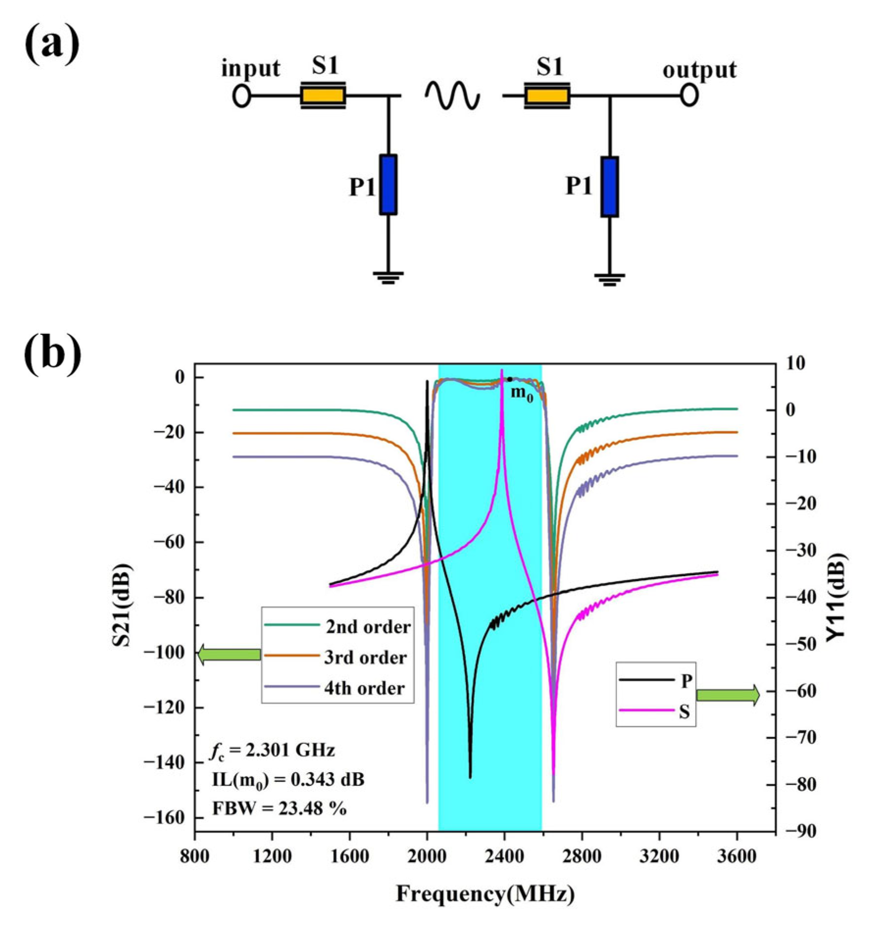
A filter prototype is implemented based on the designed resonator.
Figure 8 shows the schematic of topological structure of the SAW filter and the simulated S parameter. In this case, the ladder filter consisting of series and parallel resonators with different order is simulated. The green curve here represents the simulation results of the 2nd order circuit, and optimization was performed based on the 2nd order circuit simulation result, as the passband of the 2nd order circuit simulation result is relatively flat. As can be seen from
Figure 8a, the 3rd order circuit and the 4th order circuit are added in series based on the secondary circuit. Therefore, after increasing the circuit in series based on the 2nd order circuit. An impedance mismatch phenomenon occurs at the input port and output port, which explains the deterioration of the insertion loss within the passband. This also accounts for the more severe deterioration of the passband insertion loss in the 4th order circuit. Additionally, the presence of spurious waves in the high frequency area of the passband is due to the relatively large bandwidth of the SAW filter, causing the bulk wave of the parallel resonator to enter the passband. As shown in the
Figure 8b, the passband ripple is within a range of 1dB, which could be further optimized for a certain desired SAW filter in future work.
As can be seen, the 4th order bandpass filter offers a better rejection level of better than 30 dB, meanwhile a center frequency of 2.3 GHz, a 3-dB fractional bandwidth of 23.48% and a minimum in-band insertion loss of only 0.343 dB are simultaneously achieved, which demonstrates the applicability for wideband SAW filter with improved performance.


