Article

Research on Radiation-Hardened RCC Isolated Power Supply for High-Radiation-Field Applications

1
School of Integrated Circuits, Xidian University, Xi’an 710000, China
2
The 43rd Research Institute of China Electronics Technology Group Corporation, Hefei 230088, China
3
National Key Laboratory of Vacuum Technology and Physics, Lanzhou Institute of Physics, Lanzhou 730000, China
*
Author to whom correspondence should be addressed.
Micromachines 2025, 16(10), 1135; https://doi.org/10.3390/mi16101135
Submission received: 15 August 2025 / Revised: 21 September 2025 / Accepted: 27 September 2025 / Published: 30 September 2025

Abstract

A radiation-hardened RCC (Ring Choke Converter) isolated power supply design is proposed, which provides an innovative solution to the challenge of providing stable power to the PWM controller in DC-DC converters under nuclear radiation environments. By optimizing circuit architecture and component selection, and incorporating transformer isolation and dynamic parameter compensation technology, the RCC maintains an 8.9 V output voltage after exposure to neutron irradiation of 3 × 10¹³ n/cm2, significantly outperforming conventional designs with a failure threshold of 1 × 10¹³ n/cm2. For the first time, the degradation mechanisms of VDMOS devices under neutron irradiation during switching operations are systematically revealed: a 32–36% reduction in threshold voltage (with the main power transistor dropping from 5 V to 3.4 V) and an increase in on-resistance. Based on these findings, a selection criterion for power transistors is established, enabling the power supply to achieve a 2 W output in extreme environments such as nuclear power plant monitoring and satellite systems. The results provide a comprehensive solution for radiation-hardened power electronics systems, covering device characteristic analysis to circuit optimization, with significant engineering application value.

1. Introduction

In military electronics applications such as aerospace and aviation, various subsystems—including constant current sources, DC-DC converters, and servo control systems—require auxiliary power supplies to maintain stable operation. These systems often operate in radiation environments, one of which is nuclear radiation. Nuclear radiation environments can be classified into two categories: nuclear explosion environments and nuclear power environments. The former refers to the space where a large number of high-energy particles and intense electromagnetic pulses are generated during a nuclear explosion. The latter involves continuous radiation generated by nuclear-powered facilities such as nuclear power plants, nuclear submarines, and other platforms equipped with nuclear energy sources. In such environments, the main high-energy particles include fast neutron fluxes, high-energy electron beams, gamma rays (γ-rays), x-rays, alpha particles (α-rays), and beta particles (β-rays) [1,2]. Exposure to nuclear radiation alters the electrical characteristics of semiconductor devices due to the displacement damage effect (DDE). This effect is caused by incident radiation particles colliding with atoms in the semiconductor lattice, displacing them from their original positions and forming lattice defects such as interstitial atoms and vacancies. A vacancy and its adjacent interstitial atom are known as a Frenkel pair, while two adjacent vacancies induced by radiation are referred to as a divacancy [3,4,5]. Displacement damage can result in output voltage drift or even complete failure of auxiliary power circuits or modules, making them incapable of sustaining normal operating conditions. Conventional semiconductor devices are primarily based on silicon (Si) and fall into two categories: bipolar junction transistors (BJTs) and field-effect transistors (FETs). BJTs, being minority carrier devices, exhibit relatively strong tolerance to total ionizing dose (TID) effects from γ-rays but are highly sensitive to neutron irradiation. Key physical parameters affected by radiation include the base transit time and base width, which in turn degrade current gain, increase junction leakage current, raise saturation voltage, and reduce breakdown voltage [3], In conventional designs of DC-DC converters, bipolar devices are widely used, especially in auxiliary power supplies, and the neutron fluence threshold that bipolar devices can withstand is 1 × 10¹³ n/cm2 [6,7,8]. In contrast, FETs are majority carrier devices and respond differently to radiation. Neutron irradiation causes displacement effects that deplete charge carriers in the channel, impacting parameters such as transconductance, drain current, and pinch-off voltage. Meanwhile, γ-ray irradiation induces ionizing effects, where charge accumulation in the oxide layer at the Si/SiO2 interface introduces surface states, affecting gate leakage current and threshold voltage [9,10]. Comparatively, FETs demonstrate superior resilience to neutron-induced displacement damage compared to BJTs. Therefore, the design strategy adopted in this study emphasises minimising or eliminating the use of bipolar devices by replacing them entirely with radiation-tolerant FETs.

2. Circuit Schematic Block Diagram

The Ring Choke Converter (RCC), also known as a self-excited flyback converter, features a simple structure and low cost. It operates through self-excited oscillation, where changes in external conditions—such as input voltage or output current—can result in significant variations in operating frequency (Figure 1). This leads to reduced power conversion efficiency, making the RCC unsuitable for high-power applications.
The operating principle is as follows: When the input voltage is applied, resistor R1 provides a startup current to the switching transistor V, turning it on. The collector current IC through winding TA increases linearly, which induces a positive-top, negative-bottom electromotive force (EMF) in winding TB. This forward-bases the base-emitter junction of transistor V (base B positive, emitter E negative), quickly driving the transistor into saturation.
Simultaneously, the induced voltage charges capacitor C1. As the voltage across C1 increases, the base voltage of transistor V gradually decreases, causing the transistor to exit saturation. The collector current IC then begins to decrease, inducing an opposite EMF in winding TB (top negative, bottom positive), which reverses the base-emitter polarity (base B negative, emitter E positive) and forces the transistor to turn off rapidly.
When transistor V is turned off, no EMF is induced in TB, and the DC input voltage begins to reverse-charge capacitor C1 via resistor R1. This gradually raises the base voltage of transistor V, initiating a new conduction cycle. The circuit thus enters continuous self-excited oscillation. The waveform at the base of transistor V is a square wave with a high level of approximately 0.7 V. The capacitance of C1 determines the conduction time of the transistor, which in turn sets the switching frequency.
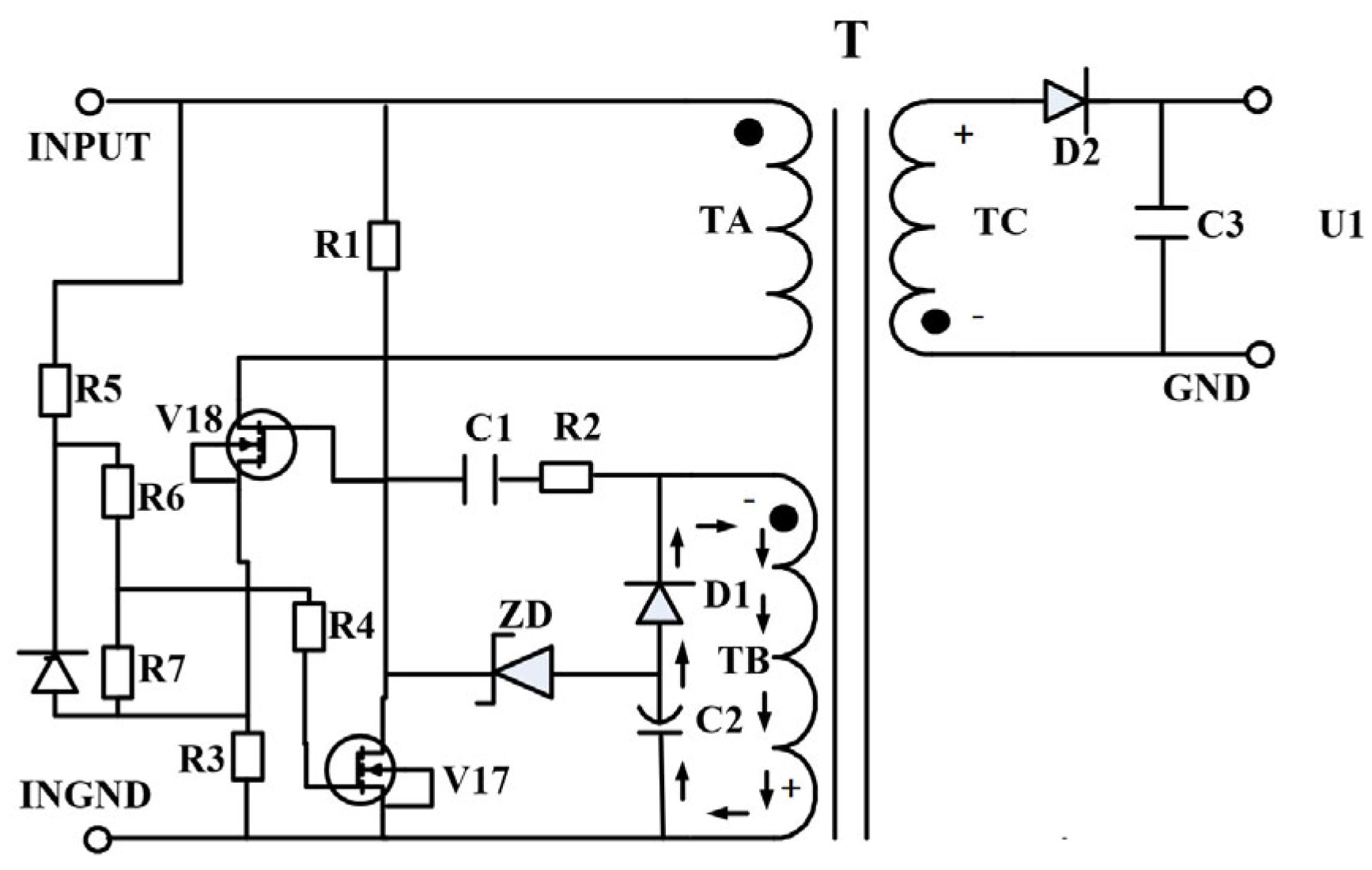
Based on the RCC’s self-excited oscillation principle, the circuit was optimized by replacing bipolar devices with field-effect transistors (FETs). A novel RCC-based auxiliary power circuit was developed, operating at a +12 V DC supply with approximately 2 W output power. The optimized circuit structure is shown in Figure 2.
As illustrated in Figure 2, the current-controlled BJT was replaced with a voltage-controlled Vertical Double-Diffused Metal-Oxide-Semiconductor (VDMOS) transistor. Both V1 and V2 VDMOS devices require a pre-driving gate-source (GS) voltage to operate correctly, enabling coordinated switching behavior. The remaining portions of the circuit remain functionally equivalent to the original BJT-based design.

3. Circuit Parameter Design

3.1. Selection of the Turns Ratio

As a boundary-conduction-mode (BCM) flyback converter, the RCC operates in a critical conduction regime. The relationship between the input and output voltage is defined by Equation (1):
N ( D ) = D × V V i n _ m i n V 0 × ( 1 D )
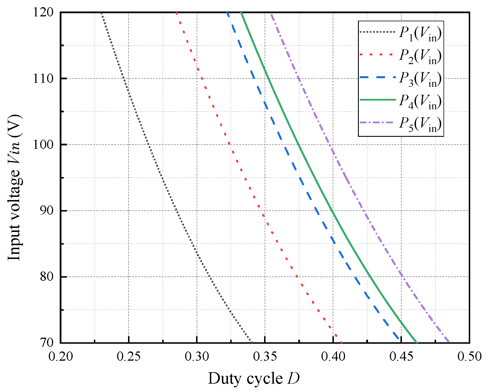
At the minimum input voltage V V i n _ m i n = 70 V, the duty cycle D typically reaches its maximum, which generally does not exceed 0.45. Figure 3 illustrates how the duty cycle D varies with the input voltage Vin under different transformer turns ratios N.
As illustrated in Figure 3, it can be seen that increasing the turns ratio shifts the curve to the right and increases the duty cycle. When Vin(min) = 70 V, the corresponding Dmax is approximately 0.45. A turns ratio of N = 4.77 is appropriate, which is rounded to an integer value of 5. The corresponding minimum duty cycle at the maximum input voltage is 0.33, resulting in a duty cycle range of 0.33–0.45, which is reasonable. Thus, Dmax = 0.462.

3.2. Frequency Selection

Based on the definition of oscillation frequency, the operating frequency f can be estimated by the following equation [11,12].
f = ( N × V 0 1 + N × V 0 V i n ) 2 × 1 2 P 0 × L P × η
Here, N = 5, V0 = 12 V, Vin = 70~120 V, Output power P0 = 2 W, A fixed time constant t is assumed for simplification.
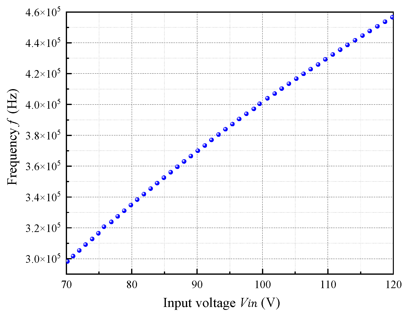
In RCC converters, the switching frequency is not strictly constant. Equation (2) shows that it dynamically varies based on input voltage, load conditions, and circuit parameters such as transformer inductance and feedback components [12]. Figure 4 illustrates the frequency versus input voltage relationship under full-load conditions, showing a positive correlation with a frequency range from 300 kHz to 460 kHz. For simplification in initial circuit design, a nominal frequency of 400 kHz is assumed, allowing estimation of inductance values, with the final output voltage adjusted by fine-tuning internal parameters.

3.3. Peak Primary Current Ip

The primary peak current Ip is calculated as:
I P = 2 × P 0 η × V i n × D
Here, the efficiency η is considered to be 60%, given the relatively low power level of the RCC circuit. At an output power P0 of 2 W, the efficiency does not exceed 65%; thus, a value of 60% is adopted. When the input voltage Vin reaches its minimum value of 70 V, the peak primary-side current reaches its maximum. Under these conditions, the corresponding duty cycle is 0.462, resulting in a maximum primary current Ip_max of 206 mA.

4. Transformer Design

The transformer uses ER7.5 series MnZn ferrite magnetic cores from Beijing Qixing Feihang. Key material parameters are:
Saturation flux density Bs = 3100 G (at 125 °C);
Remanent flu density Br = 1200 G (at 125 °C);
Effective core area Ae = 5.8 mm2;
Core volume Ve = 64.3 mm3;
(1) Primary Turns NP
N P = V i n _ min × T o n A e × B s
Calculated as NP = 44.97, rounded to 45 turns.
(2) Secondary Turns NS
N s = N p × V 0 + 0.2 V i n _ min × ( 1 D max 1 )
Calculated as NS = 9.13 N, rounded to 9 turns.
(3) Feedback Winding Turns Nf
The feedback winding must induce a voltage greater than 5.5 V [13,14]:
N f = N p × 5.5 V i n _ min
Resulting in Nf = 3.54, rounded to 4 turns. Due to space limitations, other parameter details are not elaborated here.

5. Irradiation Test Results and Discussion

The RCC circuit serves as an isolated power supply for the PWM controller within a DC-DC converter, as highlighted in the red frame of the system schematic. Neutron irradiation experiments were conducted at the Northwest Institute of Nuclear Technology. A total neutron fluence of 3 × 10¹³ n/cm2 was applied while the DC-DC converter operated under room temperature and full-load conditions.
As illustrated in Table 1 and Table 2, it is evident that the converter remained functionally stable throughout the irradiation process, validating the feasibility of using the RCC circuit to provide stable power for PWM controllers. The most significant impact of neutron irradiation is observed in the converter’s efficiency. At the nominal input voltage of 100 V, efficiency dropped from 78.2% pre-irradiation to 77.5% post-irradiation. This degradation indicates changes in the electrical performance of semiconductor components, including VDMOS switches and Schottky rectifiers.
The following analysis focuses on the impact of irradiation, specifically on the RCC converter. As a low-power flyback converter with 2 W output, its performance pre- and post-irradiation is summarized in Table 3 and Table 4.
As illustrated in Table 3 and Table 4, it is observed that both output voltage and efficiency were significantly affected by irradiation. The output voltage decreased from 12.163 V to 8.981 V at nominal input, approaching the lower operating limit (8.8 V) of the PWM controller. When neutron fluence exceeds 3.2 × 10¹³ n/cm2, the RCC output falls below 8.8 V, rendering the DC-DC converter non-functional.
To maintain operability under higher irradiation doses, the pre-irradiation output voltage of the RCC must be increased, albeit at the expense of reduced efficiency. The decline in efficiency, which suggests an increase in the on-resistance of the VDMOS devices, results in higher conduction losses. Additionally, the growing deviations in voltage and load regulation indicate reduced circuit stability, implying that neutron-induced displacement damage significantly degrades the electrical characteristics of the VDMOS.
Subsequent sections will analyse in detail the degradation trends and performance impacts of VDMOS devices operating under neutron irradiation within the RCC circuit.

6. Results and Discussion

Table 5 shows the radiation-induced electrical characteristics of the N-type irradiated power VDMOS transistors selected for the RCC circuit: Drain-source breakdown voltage: V(BR)DSS; Gate-source threshold voltage: VGS(th); Gate forward leakage current: IGSSF; Gate reverse leakage current: IGSSR; Off-state drain leakage current: IDSS; Drain-source on-resistance: RDS(ON).
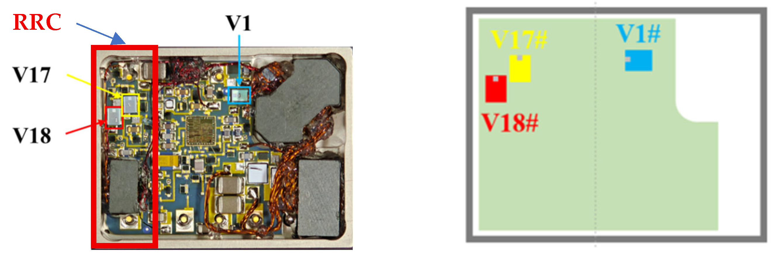
As shown in Figure 5, the power VDMOS positions in the DC/DC converter are illustrated. Here, V1 is the switching transistor of the DC/DC converter, while V17 and V18 are the power VDMOS transistors in the RCC, where V18 is the main switch and V17 is the current-limiting transistor. Testing was conducted using the Semiconductor Parameter Analyzer 4200A-SCS, with three product samples containing internal VDMOS bare chips from the same batch of fabrication. The samples were tested under full load at room temperature, and the results were averaged.
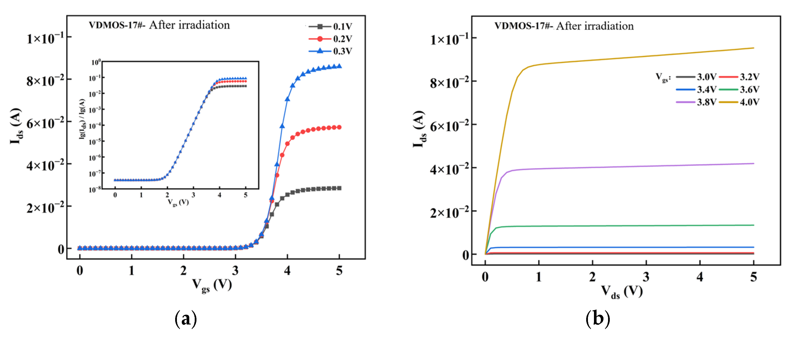
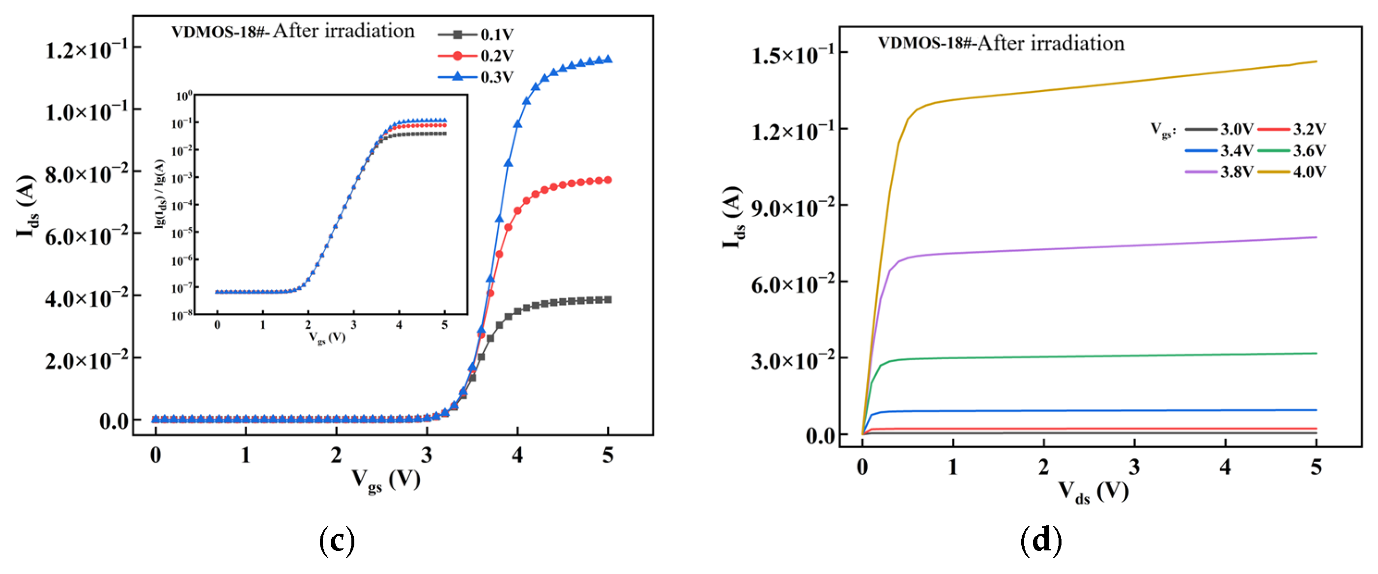
As shown in Figure 6, subfigures a and b represent the transfer and output characteristics of V17, while subfigures c and d represent those of V18. It can be observed that: after irradiation, the threshold voltage VGS(th) of V17 shifts to 3.2 V, and the on-resistance RDS(ON) increases to 1.38 Ω, while for V18, VGS(th) shifts to 3.4 V and RDS(ON) increases to 1.25 Ω. Comparing V17 and V18, both show a negative drift in threshold voltage, indicating the generation of significant oxide trap charges after irradiation. The threshold voltage of V18 experiences a smaller negative drift compared to V17, suggesting that V17 generates more oxide trap charges than V18. Furthermore, V18 exhibits a lower on-resistance after irradiation compared to V17, with similar slope characteristics in both curves and a corresponding reduction in saturation drain current.
The observed phenomena suggest that for the switching transistors in the on-state, neutron irradiation caused displacement damage. Comparative Analysis of the Differences Between V17 and V18: the extent of damage differs between V17 and V18, with V17 suffering more severe damage. This is because V18, as the main control switch, has a significantly higher drain-source current during operation than V17, which acts as a current-limiting transistor. In VDMOS devices, numerous electron-hole pairs are generated in the gate oxide, and when the current is large, a substantial number of electrons rapidly fill the traps, promoting a positive feedback effect on the electron-hole recombination rate, which reduces the damage and traps. The similar decrease in saturation drain current further suggests that the gate structure and epitaxial layer do not have a significant effect on displacement damage, consistent with simulation results from the literature [15,16].
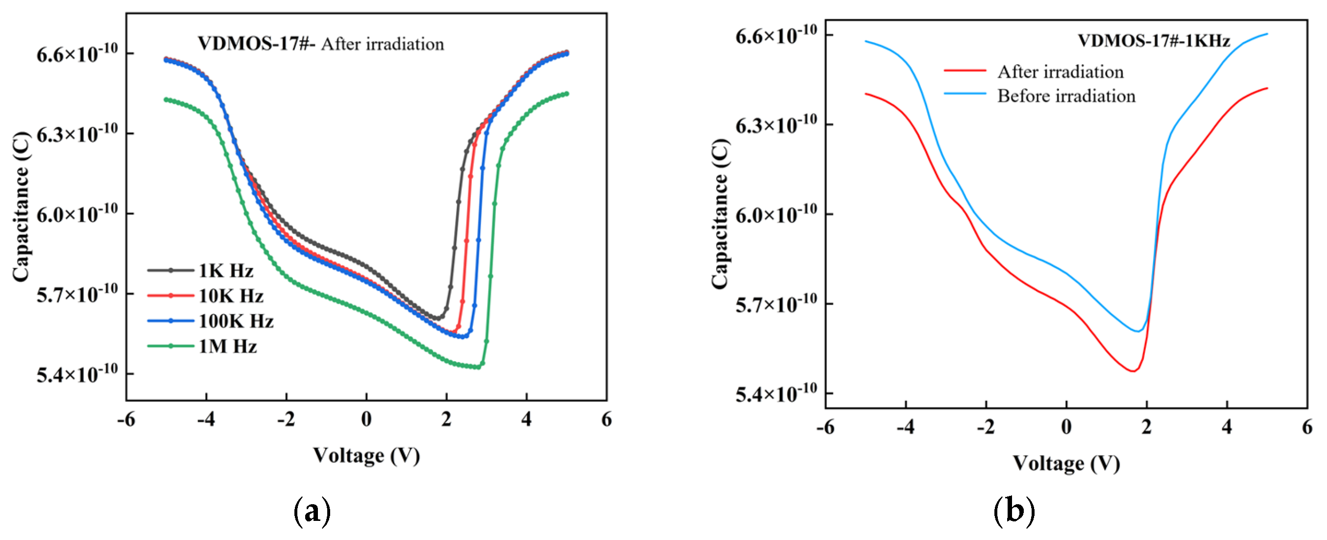
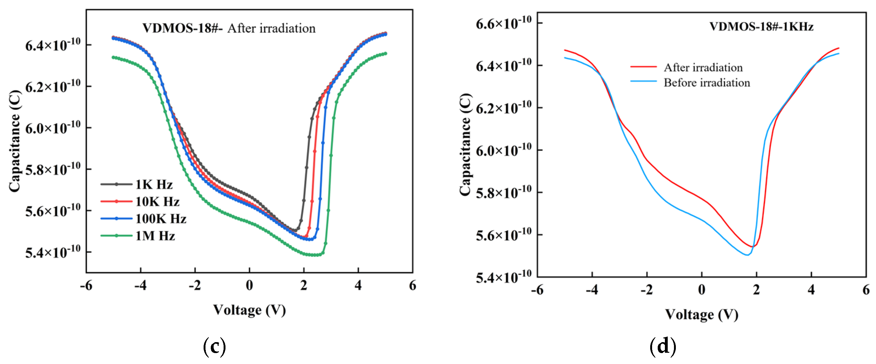
As shown in Figure 7, the MIS structure and equivalent circuit of the MOSFET are illustrated. The MIS structure consists of metal, oxide (SiO2), and silicon substrate, resulting in a gate capacitance that includes the oxide capacitance, depletion layer capacitance, and interface state capacitance. The C-V curve reflects the characteristics of these capacitances as a function of gate voltage [17,18], and it is a key method for studying the semiconductor surface and interface. Figure 8 shows the C-V characteristic curves of the MIS structure after neutron irradiation.
In an ideal MIS structure, the capacitance is equivalent to the series combination of the insulating layer capacitance and the semiconductor space charge layer capacitance. The relationship is given by Equation (7), and the equivalent circuit is shown in Figure 7.
C = 1 / ( 1 C 0 + 1 C s )
where C is the MIS structure capacitance, C0 is the insulating layer capacitance, and Cs is the semiconductor space charge layer capacitance.
From Figure 8, it is evident that the insulating layer capacitance of the VDMOS device remains largely unchanged after neutron irradiation, while the semiconductor space charge layer capacitance changes, indicating the generation of trap charges in this layer. The trap charge density in V17 is higher than in V18.
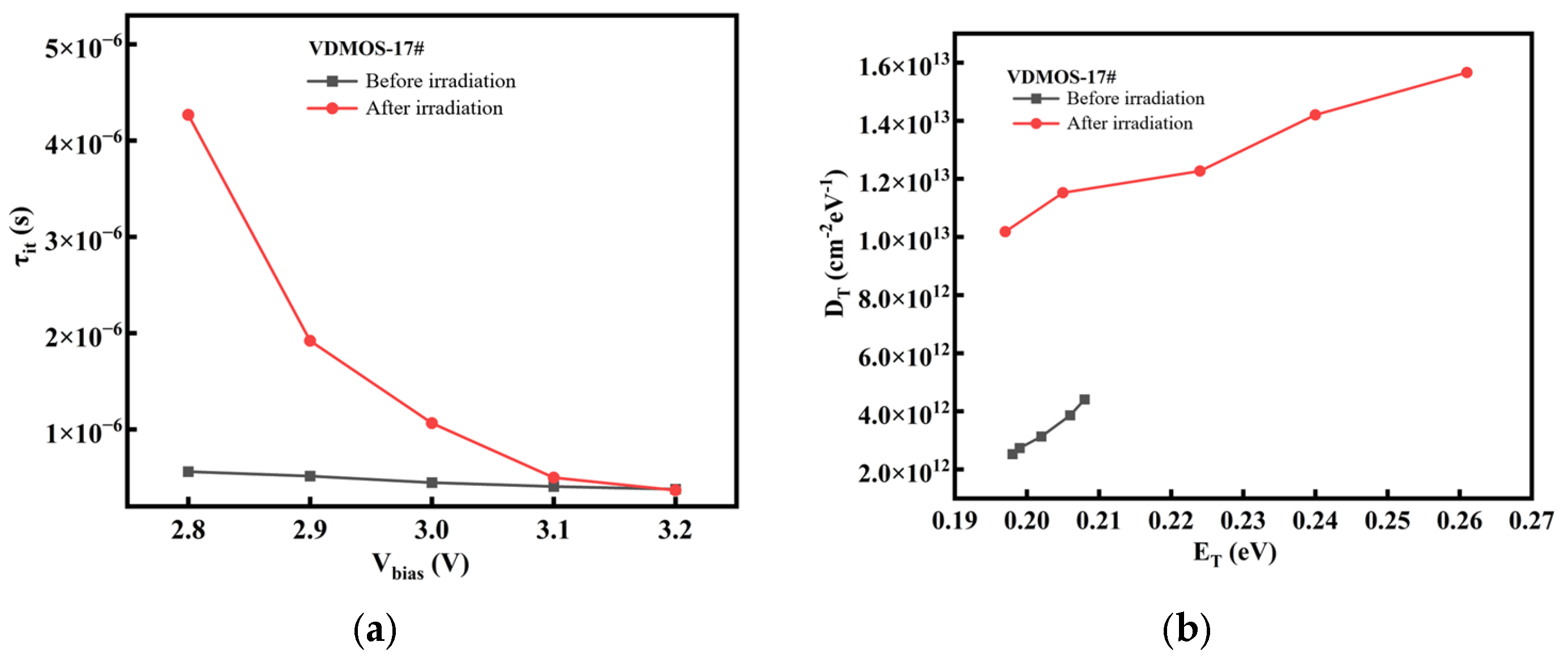
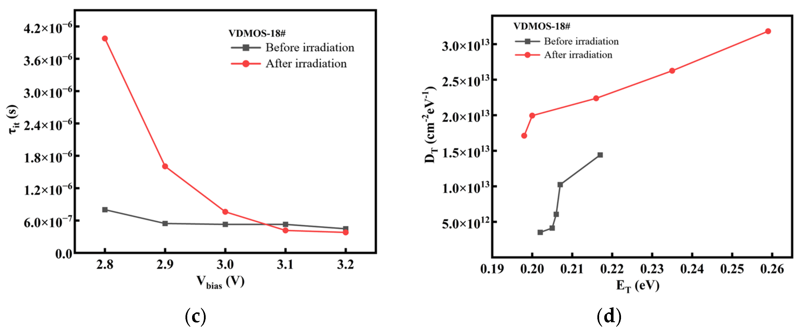
Post-irradiation, deep-level traps are formed in the VDMOS devices, as shown in Figure 9. The trap time constant increases by a factor of approximately four under low bias, meaning that once carriers are captured, their release is slower. This degrades the device’s response speed, reduces switching speed, and increases power loss. Neutron irradiation also elevates the trap density. The fast neutrons collide with silicon atoms, generating Frenkel defects that act as carrier traps. If a large number of such traps exist when the device is on, the number of free carriers decreases, leading to an increase in RDS(ON). This mechanistic explanation supports the observed degradation in electrical performance post-irradiation. Comparing the irradiation results of V17 and V18, V17 exhibits a higher concentration of radiation-induced defects and a longer trap time constant. This indicates that under cold standby conditions, devices like V17 are more susceptible to severe degradation from neutron-induced displacement effects.

7. Conclusions

A DC/DC auxiliary power supply suitable for operation in a nuclear environment was designed to power chips such as PWM controllers or FPGAs that operate within a wide input voltage range. After neutron irradiation with a fluence of 3 × 10¹³ n/cm2, the auxiliary power supply voltage dropped to 8.9 V, but the chip continued to function normally. However, to maintain a stable supply voltage during irradiation, a low-dropout linear regulator (LDO) would need to be added in the post-regulation stage. The potential drawback of this modification is a reduction in efficiency. The changes in the electrical performance of key power VDMOS devices after neutron irradiation were analyzed. Specifically, the threshold voltages of the main power switch and current-limiting switch decreased from 5 V to 3.4 V and 3.2 V, and their on-resistances increased to 1.25 Ω and 1.38 Ω. This is attributed to the fact that during RCC operation, the drain-source current of the main power VDMOS transistor is larger than that of the current-limiting transistor. Neutron irradiation causes rapid recombination of traps, which significantly reduces displacement damage. By analyzing the performance degradation of the VDMOS after irradiation, we optimized the internal parameters of the RCC. This enables the system to withstand a higher neutron fluence and extend its operational duration.
The authors wish to acknowledge Professor Zhang Maolin from Xidian University for providing semiconductor parameter testing and discussing the results.

Author Contributions

Methodology, X.L.; Validation, X.L. and H.Y.; Investigation, X.L., Y.W., and L.Z.; Writing—original draft, X.L.; Writing—review and editing, X.L., H.Y., and Y.W.; Funding acquisition, Y.W. and X.L.; Project administration, X.L. and L.Z.; Supervision, K.H., Q.H., and Z.Z.; Data curation, X.L., Z.Z., and G.D. All authors have read and agreed to the published version of the manuscript.

Funding

This research was funded in part by the National Natural Science Foundation of China (Grant No. U23A20291) and the Key Laboratory Fund (Project No. HTKJ2024KL510009).

Data Availability Statement

Data are contained within the article.

Conflicts of Interest

Youran Wu, Lihong Zhu, Ke Hong and Qifeng He are affiliated with The 43rd Research Institute of China Electronics Technology Group Corporation. The authors declare that the research was conducted in the absence of any commercial or financial relationships that could be construed as a potential conflict of interest.

References

  1. Talukder, A.; Ifty, M.R.; Al Fahad, A. Comprehensive review of GaN HEMTs: Architectures, recent developments, reliability concerns, challenges, and multifaceted applications. e-Prime—Adv. Electr. Eng. Electron. Energy 2025, 13, 101059. [Google Scholar] [CrossRef]
  2. Pan, S.; Feng, S.; Li, X.; Feng, Z.; Lu, X.; Bai, K.; Zhang, Y. Effects of 1 MeV electron radiation on the AlGaN/GaN high electron mobility transistors. J. Semicond. 2024, 45, 092503. [Google Scholar] [CrossRef]
  3. Yang, J.; Sun, X.; Yu, X.; Qin, Z.; Li, X. Characteristics of displacement defects in PNP transistors caused by heavy ion irradiation. Nucl. Instrum. Methods Phys. Res. Sect. B Beam Interact. Mater. At. 2020, 467, 86–90. [Google Scholar] [CrossRef]
  4. Ye, E.-L.; Lai, Y.-F.; Shen, C.-X.; Hou, Y.-J.; Nan, H.-J. Simulation of displacement damage in Si & SiO2 caused by protons. Radiat. Phys. Chem. 2025, 228, 112417. [Google Scholar] [CrossRef]
  5. Zimmaro, A.; Zoppo, V.; Ferraro, R.; Danzeca, S. Investigation of Radiation Effects on GaN HEMTs for Particle Accelerators. CERN Indico. 2025. Available online: https://indico.cern.ch/event/1500025/contributions/6323254/attachments/3004809/5296426/Investigation%20of%20Radiation%20Effects%20on%20GaN%20HEMTs%20for%20Particle%20Accelerators.pdf (accessed on 1 September 2025).
  6. Wang, C.; Bai, X.; Chen, W.; Yang, S.; Liu, Y.; Jin, X.; Ding, L. Simulation of synergistic effects on lateral PNP bipolar transistors induced by neutron and gamma irradiation. Nucl. Instrum. Methods Phys. Res. Sect. A Accel. Spectrometers Detect. Assoc. Equip. 2015, 796, 108–113. [Google Scholar] [CrossRef]
  7. Wu, K.; Lv, X.; Zou, D.; Lu, Y.; Li, J.; Zhao, Y. Neutron flux effect in silicon-based bipolar junction transistors exposed to californium-252. Nucl. Instrum. Methods Phys. Res. Sect. A Accel. Spectrometers Detect. Assoc. Equip. 2022, 1034, 166743. [Google Scholar] [CrossRef]
  8. Li, Q.; Lu, J.; Situ, Z.; Liu, X.; Zhang, Y.; Kong, X.; Li, C. Study of irradiation damage in silicon at different scales. Mater. Today Commun. 2024, 38, 108225. [Google Scholar] [CrossRef]
  9. Rasel, M.A.J.; Stepanoff, S.P.; Wetherington, M.; Haque, A.; Wolfe, D.E.; Ren, F.; Pearton, S. Thermo-mechanical aspects of gamma irradiation effects on GaN HEMTs. Appl. Phys. Lett. 2022, 120, 124101. [Google Scholar] [CrossRef]
  10. Hu, P.-P.; Xu, L.-J.; Zhang, S.-X.; Zhai, P.-F.; Lv, L.; Yan, X.-Y.; Li, Z.-Z.; Cao, Y.-R.; Zheng, X.-F.; Zeng, J.; et al. Failure mechanisms of AlGaN/GaN HEMTs irradiated by high-energy heavy ions with and without bias. Nucl. Sci. Technol. 2025, 36, 156–165. [Google Scholar] [CrossRef]
  11. Feng, Z.; Pan, S.; Feng, S.; Zheng, X.; Wang, Y.; Zhang, B.; Lu, X. γ-irradiation induced trapping effects on off-state and on-state p-GaN Gate high-electron-mobility transistors. Mater. Sci. Semicond. Process. 2025, 198, 109799. [Google Scholar] [CrossRef]
  12. Ravindran, R.; Massoud, A.M. An overview of wide and ultra wide bandgap semiconductors for next-generation power electronics applications. Microelectron. Eng. 2025, 299, 112348. [Google Scholar] [CrossRef]
  13. Zhang, G.; Dong, S.; Xin, Q.; Guo, L.; Wang, X.; Xin, G.; Qin, N.; Lan, X.; Guo, C.; Wang, W.; et al. Transistor-level thermal management in wide and ultra-wide bandgap power semiconductor transistors: A review. Int. J. Therm. Sci. 2026, 219, 110200. [Google Scholar] [CrossRef]
  14. Li, H.; Guo, H.; Cao, R.; Tu, H.; Huang, X.; Xue, Y.; Zeng, X. Study on electron and gamma irradiation effects and damage mechanism of GaN HEMT. Microelectron. Reliab. 2025, 167, 115616. [Google Scholar] [CrossRef]
  15. Baba, T.; Siddiqui, N.A.; Saidin, N.B.; Yusoff, S.H.M.; Sani, S.F.B.A.; Karim, J.A.; Hasbullah, N.F. Radiation-induced degradation of silicon carbide MOSFETs–A review. Mater. Sci. Eng. B 2024, 300, 117096. [Google Scholar] [CrossRef]
  16. Goud, R.S.P.; Akkanaboina, M.; Machiboyina, S.; Kumar, K.R.; Anjum, A.; Khan, S.A.; Prakash, A.P.G.; Pathak, A.P.; Rao, S.V.S.N. A study on the gamma and swift heavy ion irradiation-induced effects on the electrical properties of TaOx-based MOS capacitors. Nucl. Instrum. Methods Phys. Res. Sect. B Beam Interact. Mater. At. 2024, 554, 165455. [Google Scholar] [CrossRef]
  17. Neamen, D.A. Semiconductor Physics and Devices: Basic Principles, 4th ed.; McGraw-Hill Education: New York, NY, USA, 2012. [Google Scholar]
  18. Streetman, B.G.; Banerjee, S.K. Solid State Electronic Devices, 7th ed.; Pearson: Boston, MA, USA, 2015. [Google Scholar]
Figure 1. Schematic block diagram of a typical single-channel RCC circuit.
Micromachines 16 01135 g001
Figure 2. Optimized isolated auxiliary power supply schematic.
Micromachines 16 01135 g002
Figure 3. Relationship between input voltage Vin and duty cycle D for different transformer turns ratios N. Curves P1(Vin), P2(Vin), P3(Vin), P4(Vin), and P5(Vin) correspond to N values of 3, 4, 4.77, 5 and 5.5, respectively.
Micromachines 16 01135 g003
Figure 4. Frequency (f) versus input voltage (Vin) under full-load conditions.
Micromachines 16 01135 g004
Figure 5. Layout diagram of VDMOS.
Micromachines 16 01135 g005
Figure 6. Displacement damage effects induced by neutron irradiation: (a) Transfer characteristics of V17, (b) Output characteristics of V17, (c) Transfer characteristics of V18, (d) Output characteristics of V18.
Micromachines 16 01135 g006aMicromachines 16 01135 g006b
Figure 7. MIS structure and equivalent circuit.
Micromachines 16 01135 g007
Figure 8. C-V characteristics of MIS structures post neutron irradiation: (a) Multi-frequency C-V characteristics of V17 MIS structure, (b) Comparative output characteristics (pre-/post-irradiation) of V17 MIS structure, (c) Multi-frequency C-V characteristics of V18 MIS structure, (d) Comparative output characteristics (pre-/post-irradiation) of V18 MIS structure.
Micromachines 16 01135 g008aMicromachines 16 01135 g008b
Figure 9. Comparison of Trap Time Constants and Concentrations Before and After Irradiation: (a,b) Characteristics of V17; (c,d) Characteristics of V18.
Micromachines 16 01135 g009aMicromachines 16 01135 g009b
Table 1. Electrical parameters of the DC-DC converter before neutron irradiation.
Input Voltage (V)Input Current (A)Output Voltage (V)Voltage Variation (mV)Load Variation (mV)Efficiency
700.27512.031--77.80%
1200.16312.04312-76.50%
100 (Typical value)0.19112.038--78.20%
1000.03 (No load)12.036-2-
Table 2. Electrical parameters of the DC-DC converter after neutron irradiation.
Input Voltage (V)Input Current (A)Output Voltage (V)Voltage Variation (mV)Load Variation (mV)Efficiency
700.27712.015--77.30%
1200.16412.03116-76.10%
100 (Typical value)0.19412.017--77.50%
1000.04 (No load)12.005-12-
Table 3. Electrical parameters of the RCC circuit before neutron irradiation.
Input Voltage (V)Input Current (A)Output Voltage (V)Voltage Variation (mV)Load Variation (mV)Efficiency
700.04912.142--58.3%
1200.02612.18644-63.1%
100 (Typical value)0.03212.163--61.8%
1000.005 (No load)12.231-68-
Table 4. Electrical parameters of the RCC circuit after neutron irradiation.
Input Voltage (V)Input Current (A)Output Voltage (V)Voltage Variation (mV)Load Variation (mV)Efficiency
700.0538.805--53.1%
1200.0289.151346-58.3%
100 (Typical value)0.0368.981--56.3%
1000.10 (No load)9.183-202-
Table 5. VDMOS Electrical Characteristics.
ParametersTest ConditionsMinimum ValueMaximum Value
V(BR)DSSVGs = 0 V, ID = 1 mA150 V-
VGS(th)VDs = VGs, ID = 1 mA1.5 V5 V
IGSSFVGS = 20 V, VDS = 0 V−200 nA200 nA
IGSSRVGS = 20 V, VDS = 0 V--
IDSSVGs = 0 V, VDs = 80 V150 V 100   μ A
RDS(ON)VGs = 12 V, ID = 5 A1.5 V 460   m Ω
Disclaimer/Publisher’s Note: The statements, opinions and data contained in all publications are solely those of the individual author(s) and contributor(s) and not of MDPI and/or the editor(s). MDPI and/or the editor(s) disclaim responsibility for any injury to people or property resulting from any ideas, methods, instructions or products referred to in the content.