You are currently viewing a new version of our website. To view the old version click .
Micromachines
  • Article
  • Open Access

28 September 2025

Design of an RRAM-Based Joint Model for Embedded Cellular Smartphone Self-Charging Device

,
,
,
and
1
Computer Engineering, Brandenburgische Technische Universität, 03046 Cottbus, Germany
2
Department K-7, Jožef Stefan Institute, 1000 Ljubljana, Slovenia
3
Department of Electrical Engineering, Indian Institute of Technology, Indore 453552, India
*
Author to whom correspondence should be addressed.
This article belongs to the Special Issue Self-Tuning and Self-Powered Energy Harvesting Devices

Abstract

With the development of embedded electronic devices, energy consumption has become a significant design issue in modern systems-on-a-chip. Conventional SRAMs cannot maintain data after powering turned off, limiting their use in applications such as battery-powered smartphone devices that require non-volatility and no leakage current. RRAM devices are recently used extensively in applications such as self-charging wireless sensor networks and storage elements, owing to their intrinsic non-volatility and multi-bit capabilities, making them a potential candidate for mitigating the von Neumann bottleneck. We propose a new RRAM-based hybrid memristor model incorporated with a permanent magnet. The proposed design (1T2R) was simulated in Cadence Virtuoso with a 1.5 V power supply, and the finite-element approach was adopted to simulate magnetization. This model can retain the data after the power is off and provides fast power on/off transitions. It is possible to charge a smartphone battery without an external power source by utilizing a portable charger that uses magnetic induction to convert mechanical energy into electrical energy. In an embedded smartphone self-charging device this addresses eco-friendly concerns and lowers environmental effects. It would lead to the development of magnetic field-assisted embedded portable electronic devices and open the door to new types of energy harvesting for RRAM devices. Our proposed design and simulation results reveal that, under usual conditions, the magnet-based device provide a high voltage to charge a smartphone battery.

1. Introduction

Recently, many unique memory techniques have been investigated [1]. Integrated circuits’ ongoing reduction in cost and power consumption has been the primary driver of the explosive growth in portable electronic devices. The prospective flow of hybrid technology is predicted to be a leading-edge technology in the forthcoming years [2]. In this situation, resistive random-access memory (RRAM) is a possible contender for next-generation Non-Volatile Memory (NVM) technology [3]. This technology is defined by its accessible structure, quick switching speed, great scalability, and integration ability at a standard CMOS process’s Back-End-Of-Line (BEOL) [4,5]. As a cutting-edge electronic component, the memristor has enormous potential for energy-efficient technologies in the future, especially for embedded electronic portable systems [6]. The research for memristor devices with excellent energy efficiency is still ongoing, and a recently created self-generating technology that can capture different types of environmental energy to power functional components showed commitment [7]. An external-power-supply-source dependence is eliminated by this self-powered technology. This self-powered memristor gadget satisfies the consequence approach and application prerequisites of green electronics and has the benefits of being environmentally benign, sustainable, and renewable [8,9]. The literature survey indicates that integrating and combining several devices is a potential technique for multipurpose, power-free, smart electronics [10]. This new device element has gained a widespread adoption and a lot of popularity in recent years because it has the potential to integrate these self-powered systems with other functional devices and power-free electronics, like self-powered motors, sensors, detectors, generators, and energy-efficient memristive systems [11].
Over the past few years, numerous researcher have developed a variety of self-powered technologies that sense physical conditions, including moisture-powered memristive systems and various technologies [12]. The aforementioned power-free electronics systems served as inspiration for the incorporation of memristors, the fundamental sensor unit, into self-powered technologies [13]. In further research and development, memristor-based solutions may open the door to more environmentally friendly and self-sufficient mobile devices, revolutionizing smartphone powering and drastically lowering the demand for conventional charging techniques [14]. Therefore, wireless sensor nodes require alternate charging sources. The literature has proposed generators based on piezoelectric [15], electromagnetic [16], and electrostatic [17] conversion. Therefore, developing self-powered memristive devices would be highly relevant and remarkable.
This study presents a memristor model for an internal generation system for self-charging a smartphone’s battery. Self-powered embedded portable devices are architecturally constituted of an electromagnetic nanogenerator and a memristive division which are connected together in series [18]. This concept can serve as the building block for a conventional SRAM cell if a higher resolution is achieved with a self-powered memristive device to investigate the modeling and design of a magnetic induction caused by an oscillating permanent magnet mechanical-to-electricity converter to be used as a power source for the wireless self-charging devices. The reader is referred to the concept of the work by A. Vishwakarma et. al. [19,20,21] for a discussion of associated self-powered charging electronic devices. Although others have proposed the idea of using an RRAM device within an optimized CMOS memristor-based cell [22], these implementations are merely proposed as a concept, using an existing and specific RRAM device [22,23]. Our research is focused on the simulation application of the RRAM model device. By combining it with a magnetic field, we aim to generate enough output voltage for edge devices, making it an ideal fit for smartphone self-charging applications. A self-generating memristive system such as this may open up a whole new field of study that could significantly advance the creation of new technology.
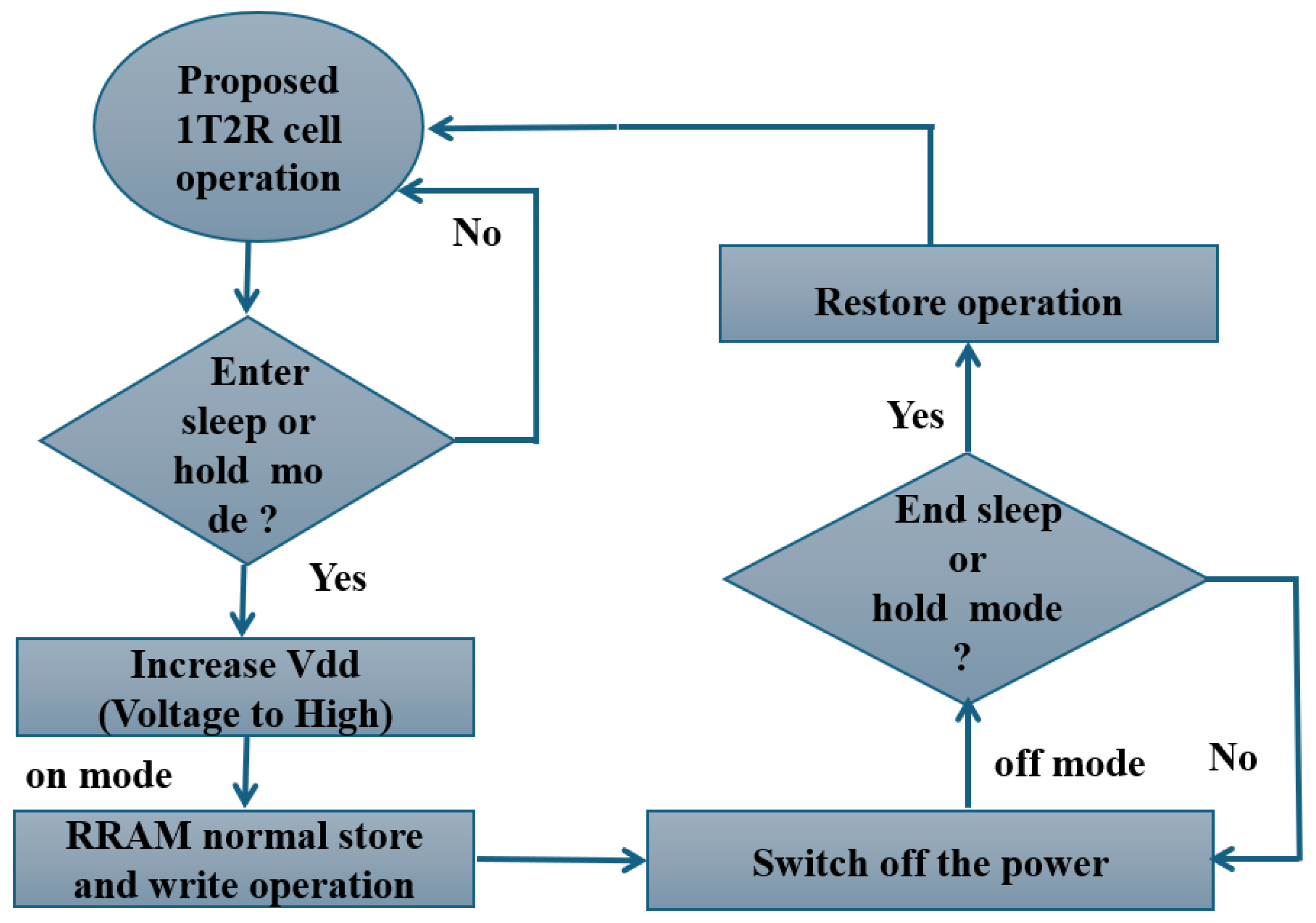
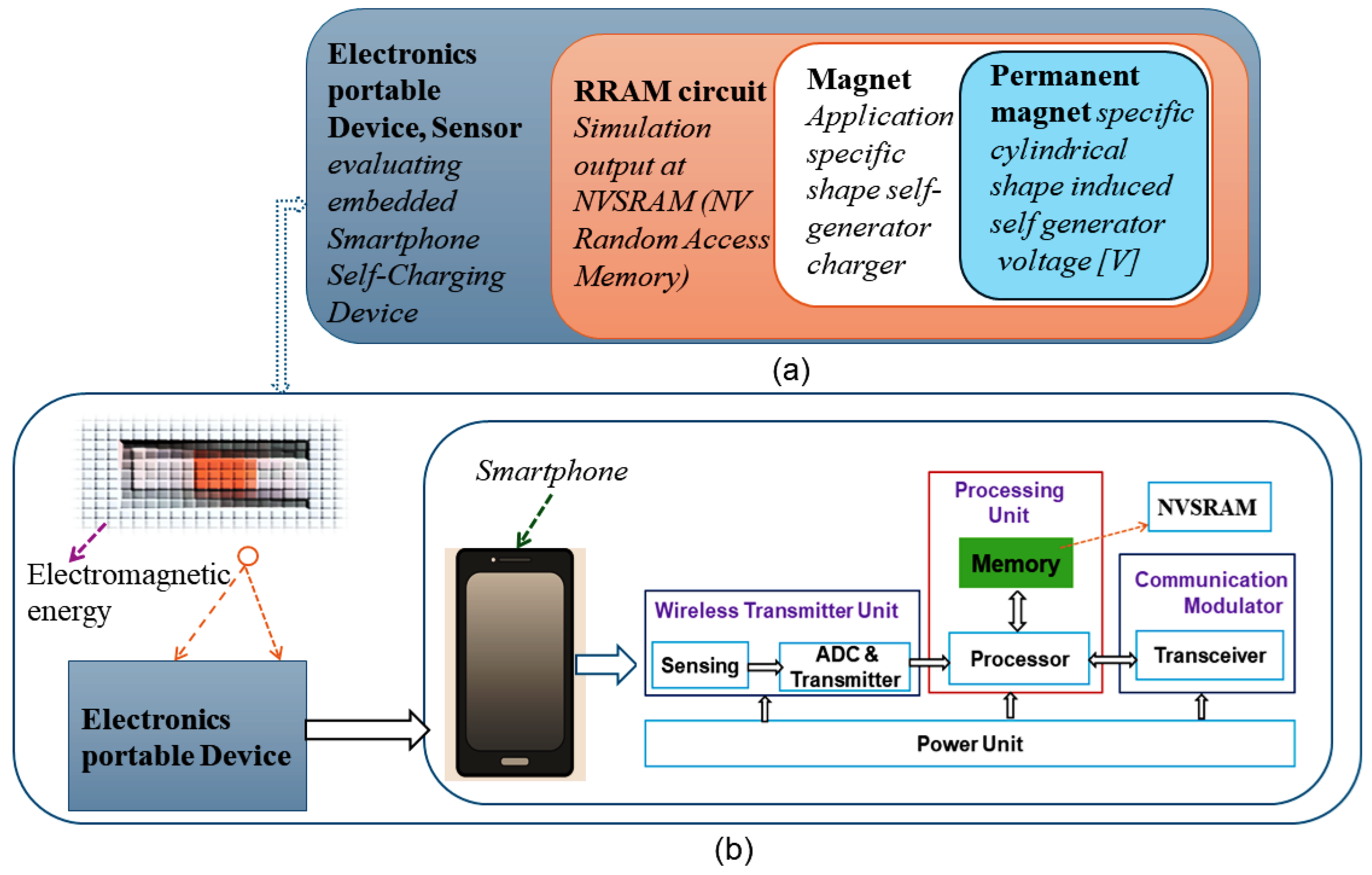
As a proof of concept we simulate the operation of RRAM units, included in a portable, smartphone-like device, schematically presented Figure 1a: A circuit-level integration approach for RRAM-compute blocks for self-energy generation Figure 1b SoC Block diagram of various modules of the wireless smartphone self-charging device. The simulation of the RRAM device uses a 1T2R cell design with an optimized cylinder-shaped permanent magnet; the proposed concept shows the auto energy generation for wireless smartphone self-charging applications. Hence, an improvement in total power is obtained. In this study, we present an implementation that consists of a memristor-based 1T2R optimized using IHP 130 nm SG13S technology and prove the concept by means of the finite-element magneto-static simulations that allow for the combination of RRAM device technology into CMOS designs.
Figure 1. (a) Proposed concept: A circuit-level integration approach for RRAM-compute blocks for self-energy generation. (b) SoC Block diagram of various modules of the wireless smartphone self-charging device.
This paper presents the following essential features:
  • The proposed IT2R RRAM cell operates better than the previous design [22,23] in terms of write/read time and power consumption, and combining RRAM with IT2R cells is more efficient than using conventional memories.
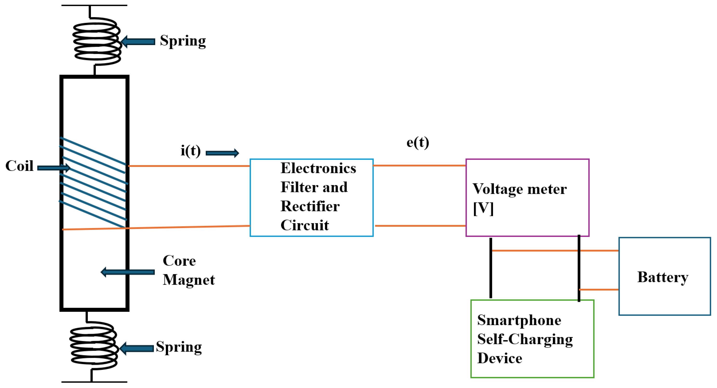
  • The suggested concept [19,20] is to generate self-energy by magnetic induction from a permanent magnet oscillating inside a coil.
  • The successful simulation of the joint RRAM device and the proposed in-built permanent magnet validates its potential for smartphone self-charging. applications.
The rest of the paper is structured as follows: We introduce relevant topics, background, and related work in Section 2. Section 3 presents the methodology used for implementation. We evaluate the simulation and discuss the results in Section 4 and conclude the paper in Section 5.

3. Methodology

In this section, we explain how we constructed an optimized 1T2R (one-transistor-two-resistor) and extended the circuit toward a permanent magnet transition into a device with self-energy generation. This approach demonstrates significant progress in developing efficient, self-charging embedded electronic devices.

3.1. Concept

This section is concisely and precisely describes the Conventional 6T SRAM cell and proposed design structure.

3.1.1. The Conventional 6T Cell

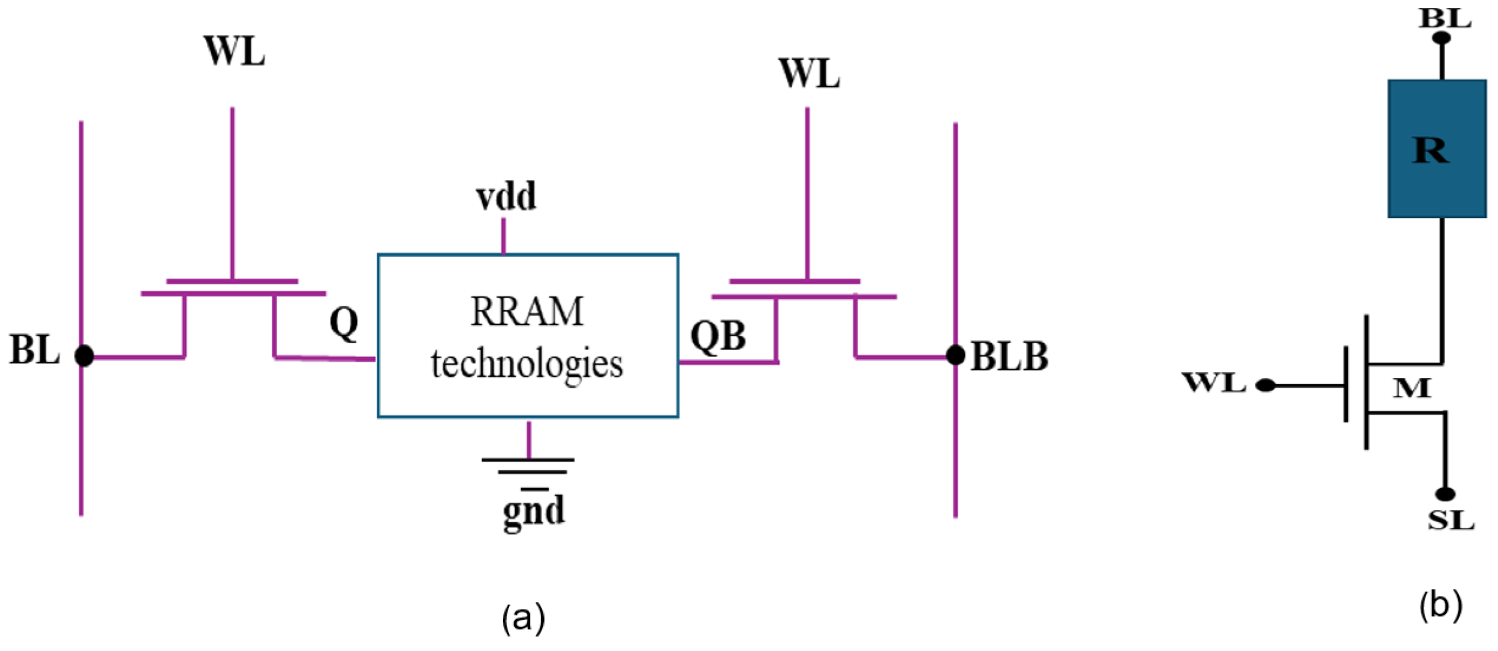
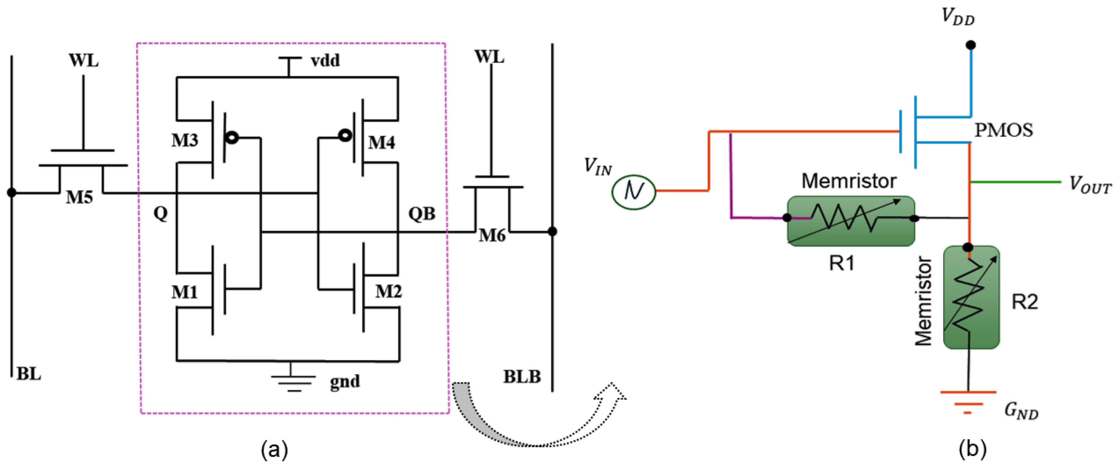
A single SRAM memory cell consists of six transistors (M1, M2, M3, M4, M5, and M6). A standard SRAM cell is formed by a latch (using two cross-coupled inverters) and two access transistors. Figure 8a depicts a schematic view of conventional 6T SRAM, with the cross-coupled inverters M1–M3 and M2–M4 [10]. The two access transistors, M5 and M6, are coupled to the complementary bit lines BL and BLB. The primary operations of an SRAM memory cell are hold, read, and write, which are carried out using Word Lines (WLs) and Bit Lines(BLs). Every SRAM cell has the potential to store “0” or “1”. WLs are connected to the gates of the selected transistors (M5 and M4), while BLs are attached to the transistor terminals. During the hold stage, the WLs are deactivated, disconnecting the BLs from the SRAM core [1]. Data is stored in the latch structure on data nodes Q and QB [5]. WL is activated to perceive or update the stored data in order to complete read and write activities. An SRAM has three major operations: hold or standby, read, and write mode.
Figure 8. (a) Conventional 6T SRAM cell structure [10] (b) Proposed 1T2R RRAM-based structure.
  • Hold or Standby mode: During standby mode, the world line signal deactivates the access transistors, disconnecting the bit lines voltage from the storage nodes [42].
  • Read Mode: During read operation, the WL signal remains active to switch on the access transistors, and the bit lines are pre-charged to vdd. The storage node Q supplies a discharge channel to the matching bit line BL, and the sense amplifier at the read output port detects the voltage difference between the two bitlines [10].
  • Write Mode: The bit line is used with the value of be stored in SRAM. The world line control signal activates the cell through the access transistors, which can change the last state of the cross-coupled inverter with the weaker transistor. Therefore, the substitute value is saved [42].

3.1.2. Proposed 1T2R Structure

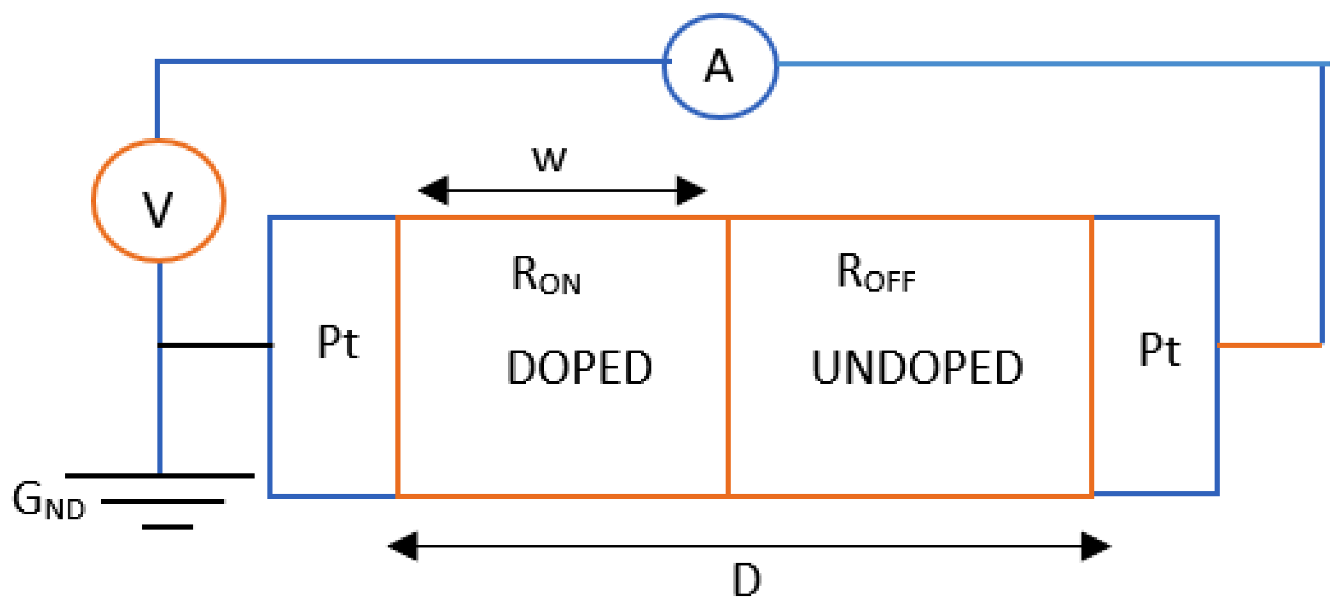
In this section, we introduce the proposed schematic of the 1T2R design in cadence virtuoso 130 nm software, as illustrated in Figure 8b. This architecture has been invented using twin memristors (R1 and R2) and a transistor. It is a volatile memory device with cross-coupled inverters (seen in Figure 8a), which are replaced by the RRAM-based design and the storage units of this circuit, which act as two access transistors. The proposed circuit employs a single P-channel metal oxide semiconductor (PMOS) and dual memristors (R1 and R2) instead of an NMOS with a lower threshold voltage to increase switching speed. The design comprises a series of PMOS transistors associated with an insulator-metal. Memory units regulate the current that flows via PMOS and are utilized for recent feedback. The provided voltage V D D is connected to the PMOS transistor’s source terminal, as indicated in the schematic—these mechanism designs, including memristor R1, serve as a feedback branch. This circuit are simulated using the usage window function in conjunction with the linear boundary drift model. We utilized the Stanford PKU memristor model parameters as described in [39,43] and illustrated in Table 1. The details of the conventional 6T SRAM design part have been clarified in the earlier section. Conventional SRAM can perform only read, write, store, and write/write activities, While NVSRAM can read, write, store, and recall. Table 2 shows the transistors’ dimensions and the parameters fed to the memristor model to simulate the behavior of the IHP’s 130 nm technology RRAM cells. While others have already suggested this idea and the subsequent equations [22,23], we contribute by extending this idea to a particular CMOS process and a specific RRAM device. Afterward, the second memristor (R2) is applied to connect the output node to the ground. In the previously mentioned states of our circuit, this memristor is positioned to regulate the voltage division and the PMOS transistor’s passing current. The positive terminals of the memristors, R1 and R2, are connected to the output node. This circuit uses a PMOS as a switching component. Because V D D is constant, the PMOS switch’s on and off states are scheduled using the input voltage V I N . The current will flow through the memristor with activation of R O N if the input voltage V I N is adjusted to zero, placing PMOS, R1, and R2 in an on state (shown in Table 2). If the source-to-gate voltage falls lower than the PMOS threshold voltage, memristor R1 switches off while R2 remains on, indicating a PMOS cutoff. When V I N = 0, the transistor enters the on-state, extracting Equation (4), indicating the output voltage described below [22,23], where Req is the corresponding memristance of the memristor.
V 0 U T = R e q · I D
V 0 U T = ( R 2 R 2 + R 1 ) · V 1 = ( R O N R O N + R O F F ) · V 1
Table 1. RRAM model specifications [39,43].
Table 2. Memristors with different voltage and dimension valves.
Consequently, it is possible to ascertain the PMOS transistor’s passing current and output node voltage. According to our memristor model, the R O N and R O F F values are different. Both memristors stay in the on state because the current flows to their positive sides. Memristors with identical resistance and current could be used to extract an output power, which would be 1.5 V at that level. If 1.5 V is the input voltage, the condition will change. If the voltage difference (VSG) is less than the edge voltage (VTP) of the PMOS transistor, the PMOS switch is off. While memristor R2 stays in the on position, memristor R1 stays in the off position due to the electrical current produced by the input voltage. Acquiescent resistance R O F F generates a circumstance with no current flow. In (3), the voltage output is as follows [22,23]. By changing the actual values of R O N and R O F F , it is clear that the result node is set to roughly 0 volts. In other words, such a design approach aims to achieve the same goal as the perfect ideal non-volatile output. The simulation results are presented in the next section.

3.1.3. Proposed Novel Schematic Design for the Self-Energy Generator

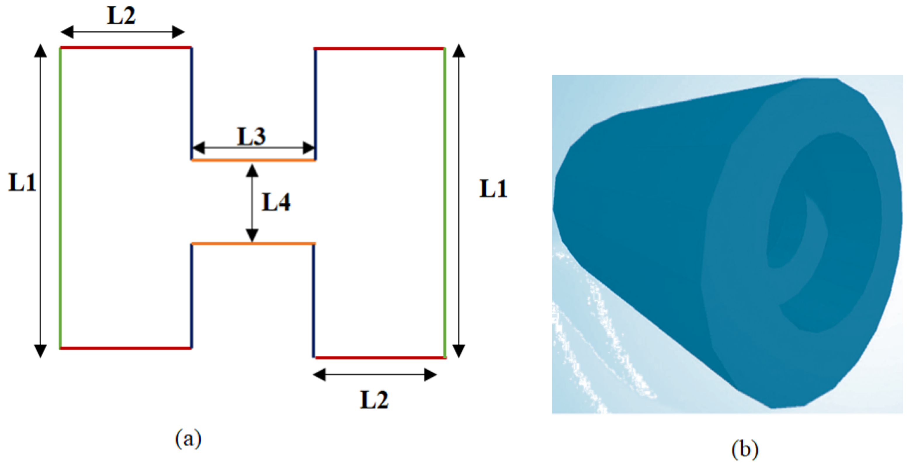
The main idea is to use a single magnet of a specially-designed shape, magnetized uniformly in one direction. In Figure 9a, we illustrate the shape and structure of our proposed permanent magnet. The cylindrical shape with notches (Figure 9b) under consideration allows for the adherence to a planar problem because of its rotational symmetry. Table 3 displays the geometric details.
Figure 9. (a) The schematic and dimensions represent the proposed permanent magnet generator. (b) The proposed shape of the magnet.
Table 3. Geometry specifics for the proposed magnet dimensions.
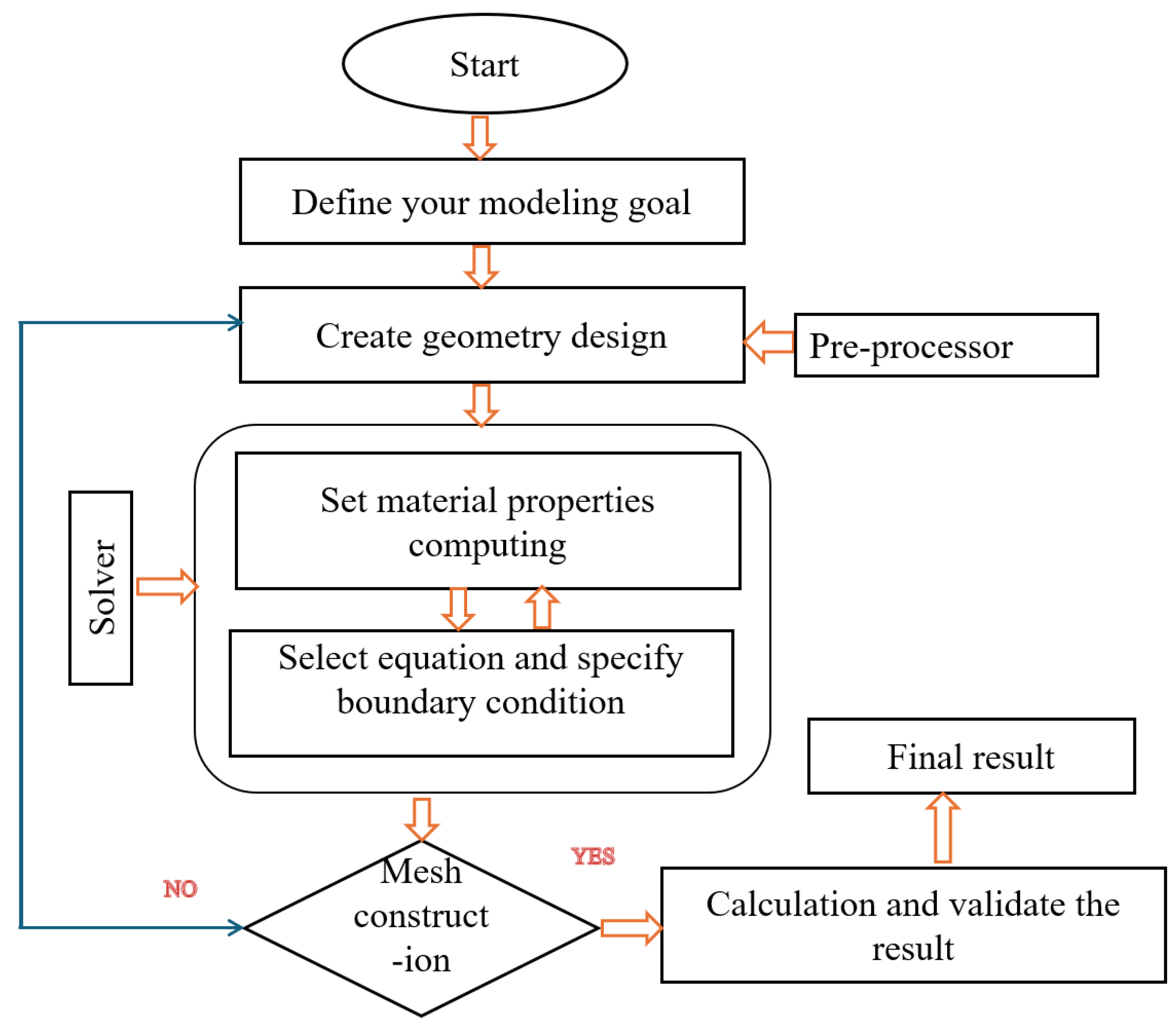
Figure 10 depicts the entire procedure diagram for the magnetization representing technique. We adopt the magnetic characteristics of a cutting-edge sintered magnet (NdFeB-50) with a high enough remanent magnetization. The specially designed notches in the magnet reduce the weight and improve the required inhomogeneity of the resultant field, even for uniaxial magnetization, as shown in Figure 11, which is essential for a non-zero time derivative in Equation (1).
Figure 10. Detailed flow procedures for the magnet-modeling.
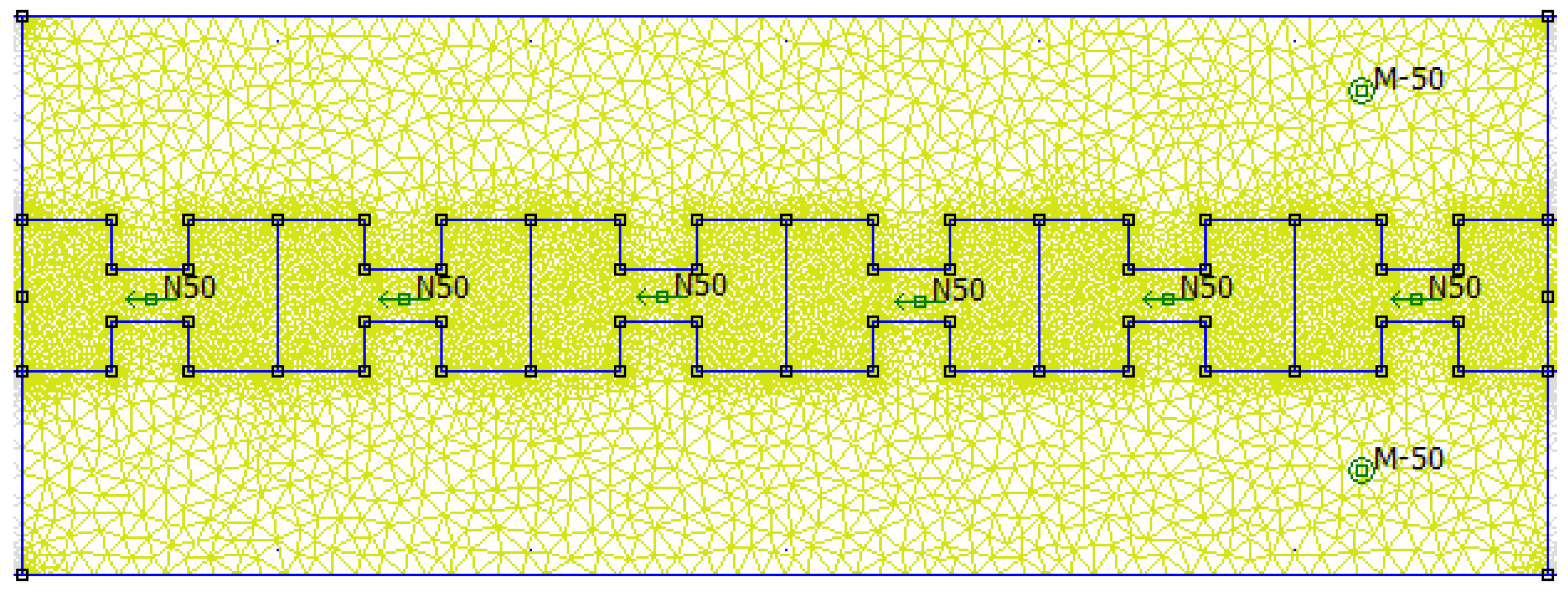
Figure 11. The software design schematic represents the proposed permanent magnet self-energy generator, with green arrows indicating magnetic direction.
The FEMM software (https://www.femm.info/wiki/HomePage) was used to perform FEM computations of magnetic-flux density. The mesh design and application of the boundary constraints must require special consideration. A triangular mesh and the first-type (Dirichlet) boundary conditions were used. The convergence tests were used to calculate its density [20]. The meshing for the magnet geometry under consideration is shown in Figure 11. The mesh structure is tighter toward the magnet’s surface, where field gradients are more pronounced. The time dependence of the calculated flux is modeled by examining various displacements between the coil and magnet while assuming harmonic motion [19]. To simplify the process, the angular frequency was fixed to ω = 1 s 1 . Equation (1) is carried out in terms of a finite-difference method to the time derivative, and Equation (2) applies the average value B of the magnetic flux density for a given cross-section. The main advantage of these suggested magnets is that they produce a sufficient voltage for charging an electronic device battery in normal circumstances. The evaluations are presented in the next section.

4. Simulation Results and Discussions

4.1. 1T2R RRAM Simulation

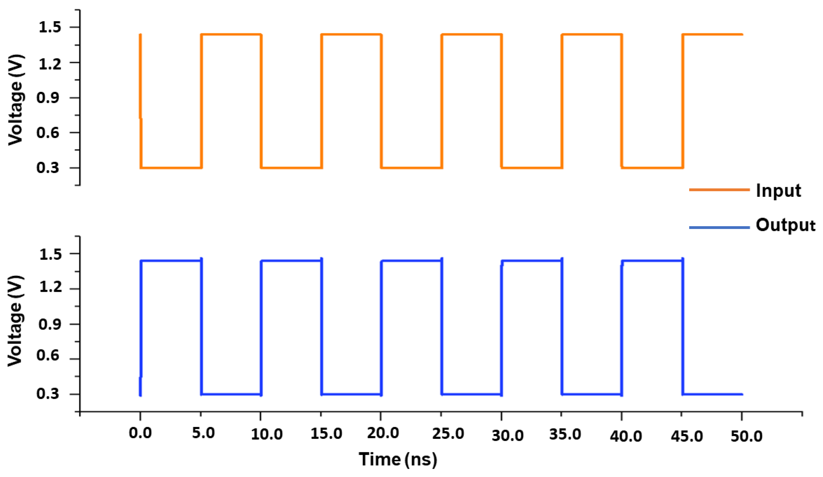
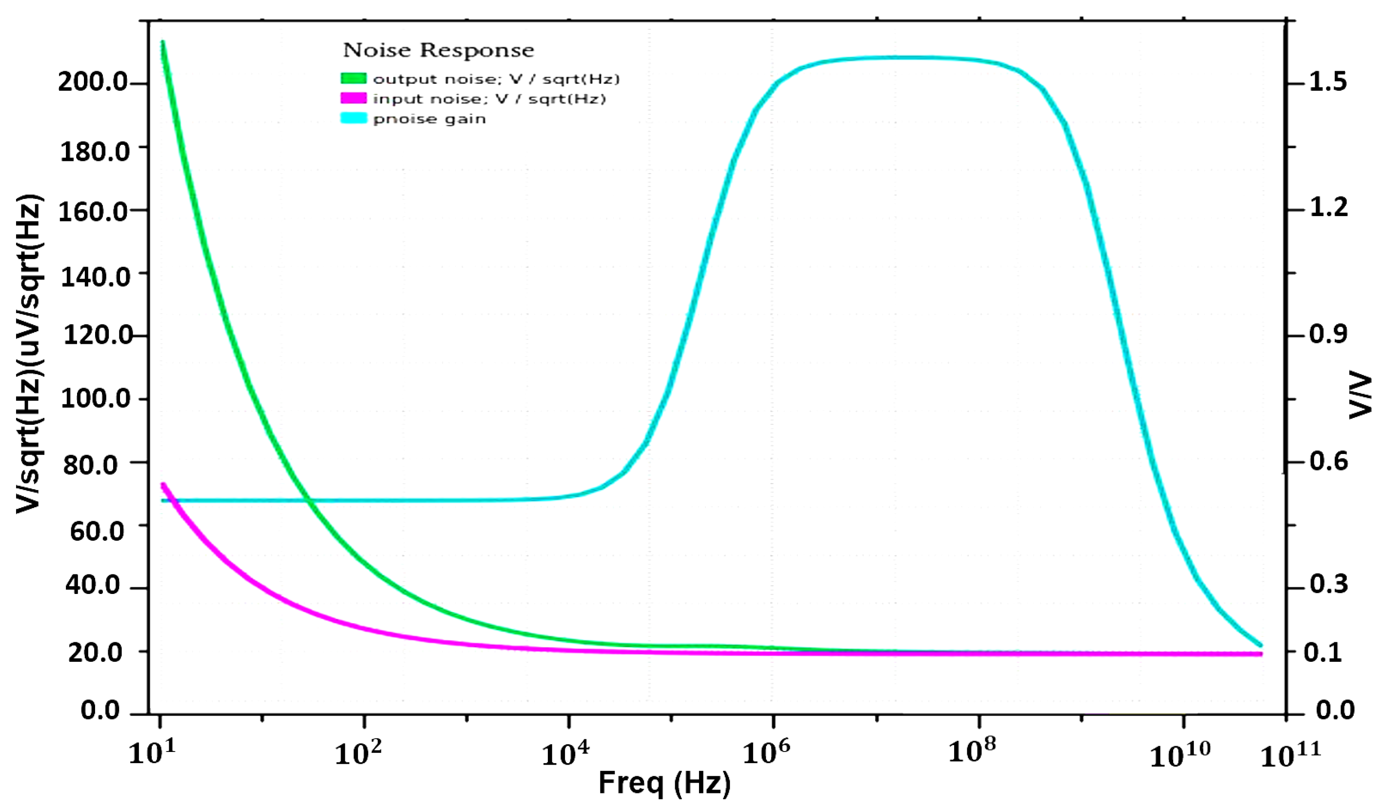
This part demonstrates the usefulness of optimizing our proposed structure for usage with RRAM electronic devices. As previously explained, the suggested 1T2R architecture can keep its pre-programmed state, operating similarly to traditional SRAM cell behavior. The designed 1T2R and other reference circuits have been modified and simulated using industry-standard 130 nm CMOS technology and device size. The simulation results given were obtained using Cadence Virtuoso. The entire simulations are performed considering 1.5 V of the input voltage at the operational temperature of T = 27 °C while consuming a total power of 17.67 µW. A memristor-based feedback system has been used to analyze the read/write operation and non-volatility output. The circuit has a non-volatile output that is memristor-received. To examine the non-volatility characteristics of the proposed design, the most critical concerns, such as read and write time concerns, should be kept in mind. The output memristor (R2) is connected to the input memristor (R1) through a feedback-wired loop network. As in the state of R1, the input values are defined. The voltage at the output node is tuned to around 0 volts whenever the actual values of R O N and R O F F are substituted. This indicates that the circuit functions similarly to an ideal inverter. The transient analysis of the presented design is displayed in Figure 12. The rise and fall times are 5 ns. The various memristor variables for V I N = 1 and V I N = 0 and the proposed design based on memristor are shown in Table 2. The writing term is the shortest possible duration of time the input pulse must have been present for the memristor state to change from w = 0 ( R O F F ) to = D ( R O N ) [23]. In the suggested circuit, the R2 memristor will stay at R O N after the write time has elapsed. Following the writing time, if the input voltage V I N causes the output response for V O U T = 1, the memristor R1 will change. In this particular scenario, all memristors are enabled. Whenever V O U T = 0, the memristor condition is fixed allowing the significances in Table 2. Under these circumstances, R2 is on and R1 is off. In this case, the zero output value is expected. Figure 13 displays the simulation outcome for this condition. It will be beneficial in defining the circuit’s routine as well as the memristor R1’s intended function as an SRAM cell. Circuits develop non-volatile performances as a result. Figure 14 presents the noise performance simulation results, illustrating the impact of input-referred noise, output noise, and phase noise margin for the suggested design. The correlation between frequency (Hz) and V/sqrt referred noise (V/Hz) is displayed in the graph plot. Table 4 shows the measured parameters of the presented RRAM design. The suggested system design is an innovative concept that focuses on efficient memory utilization for self-charging devices.
Figure 12. Transient analysis of the proposed design.
Figure 13. Proposed design non-volatile output write time analysis.
Figure 14. Noise response of our design.
Table 4. Simulated parameters of the suggested design.

Monte Carlo and Voltage Transfer Characteristic Simulation

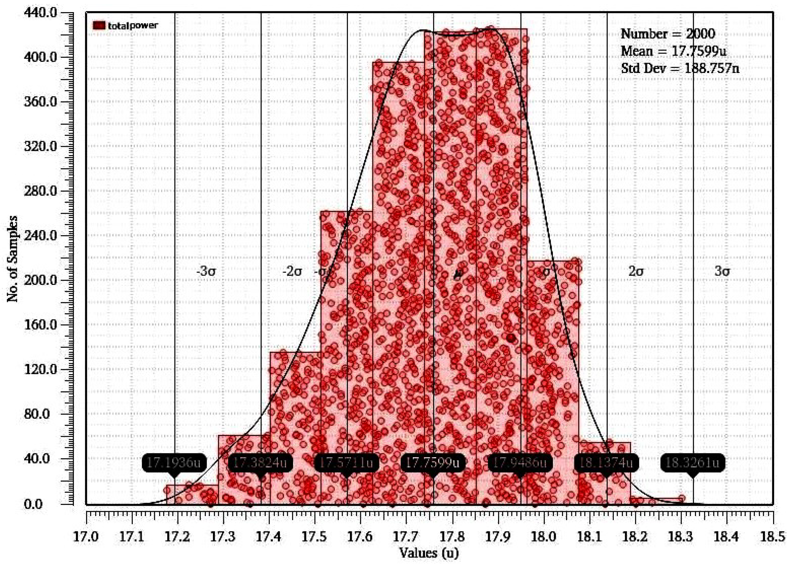
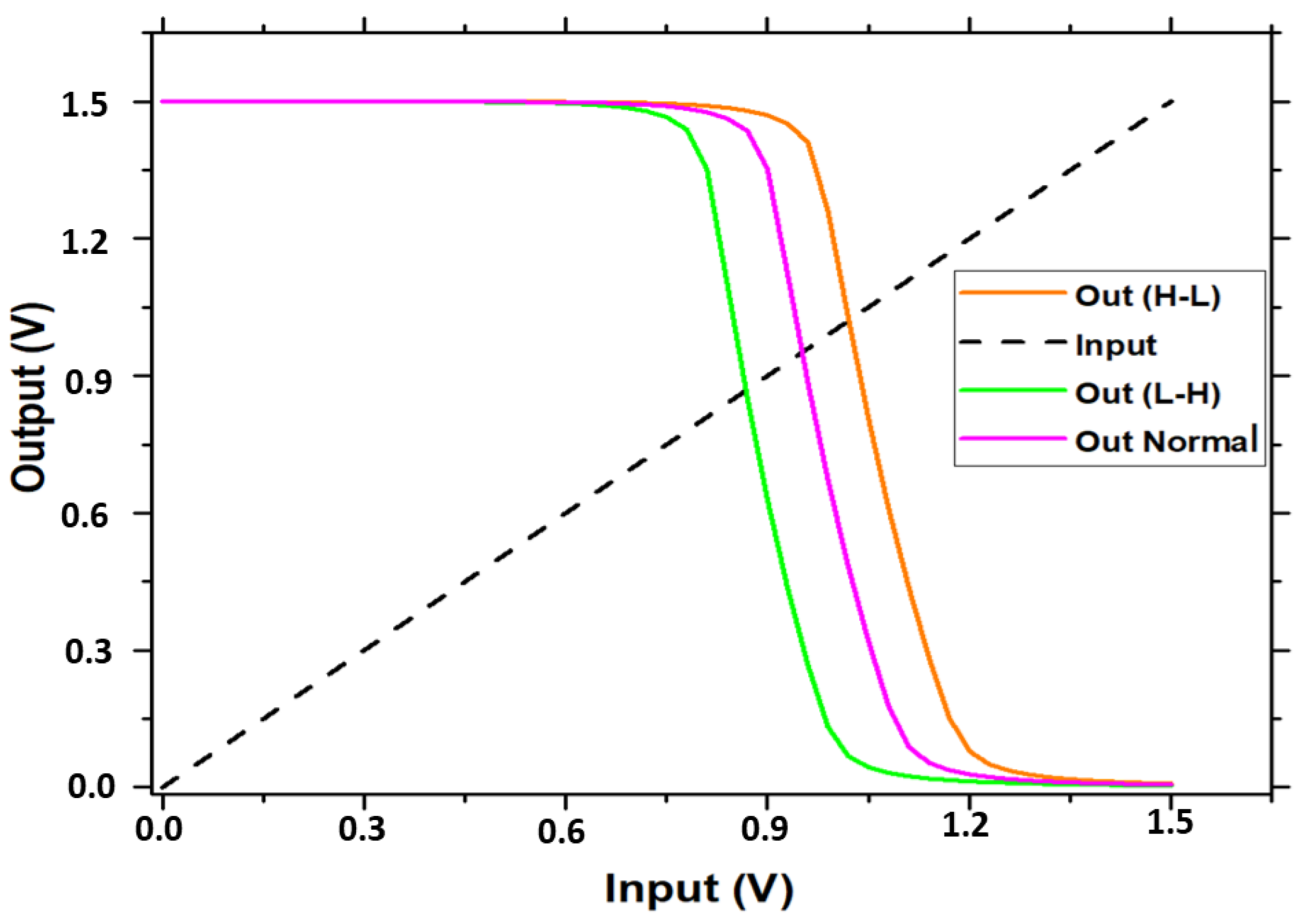
Monte Carlo (MC) is a popular statistical technique for calculating the probability of certain events under an unknown distribution. Figure 15 shows the results of Monte Carlo simulations of 2000 samples for the total power utilization of the suggested RRAM memristor-based design under different processes and mismatch operations. The overall power usage is around 17.75 µW, with a minor standard deviation of 1.85 µ. We evaluate the hysteresis curve for the proposed circuit, as depicted in Figure 16, and point to the outputs H-L and L-H. This curve demonstrates enhanced performance when bootstrapping the voltage drop. These circuits under consideration have a high-to-low voltage transfer characteristic (VTC) transition. H-L and L-H are the circuit’s upper and lower threshold voltages; outnormal is the input and output crosspoint voltage. Table 5 presents a comparison between the suggested RRAM (1T2R) design and designs that have been proposed in the literature.
Figure 15. Power consumption results from Monte Carlo simulations.
Figure 16. Voltage Transfer Characteristic of our design.
Table 5. Compared the proposed design to those proposed in the literature.

4.2. Magnet Self Generator Optimizations

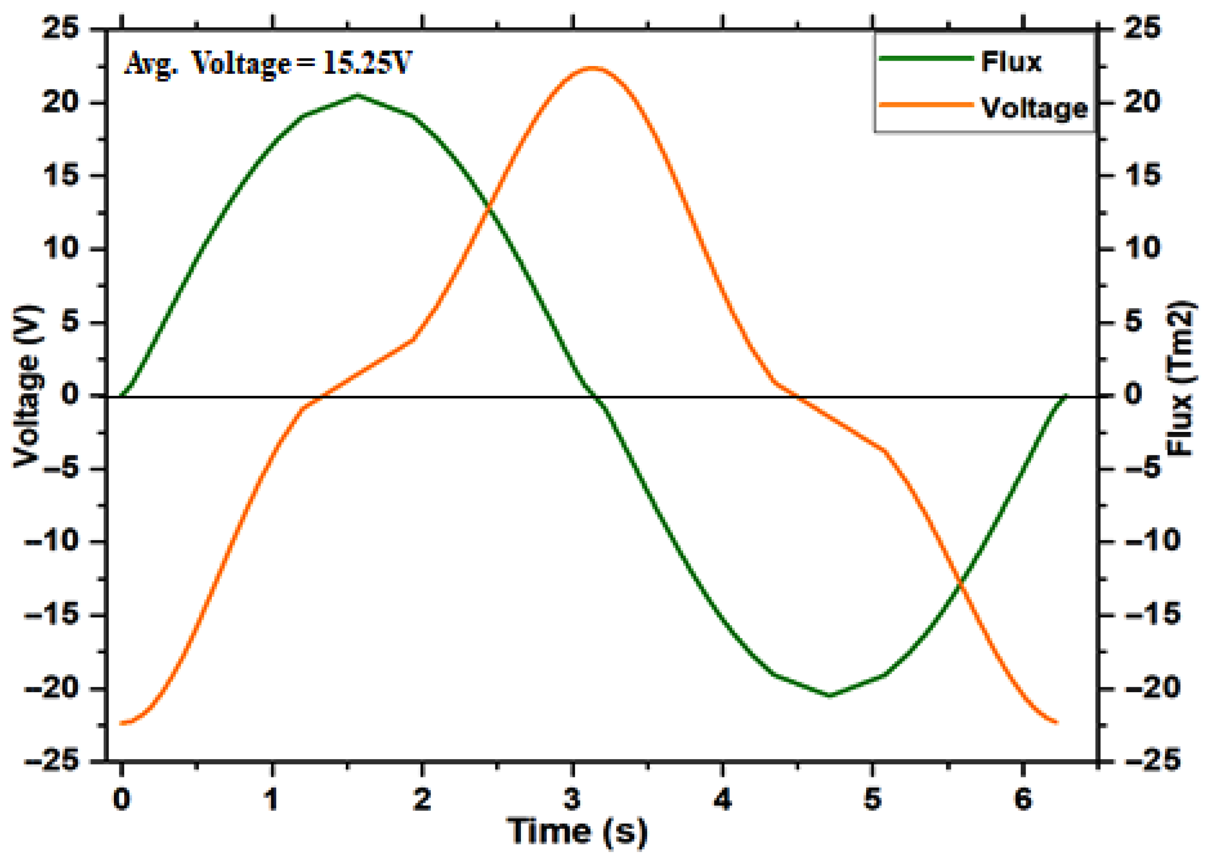
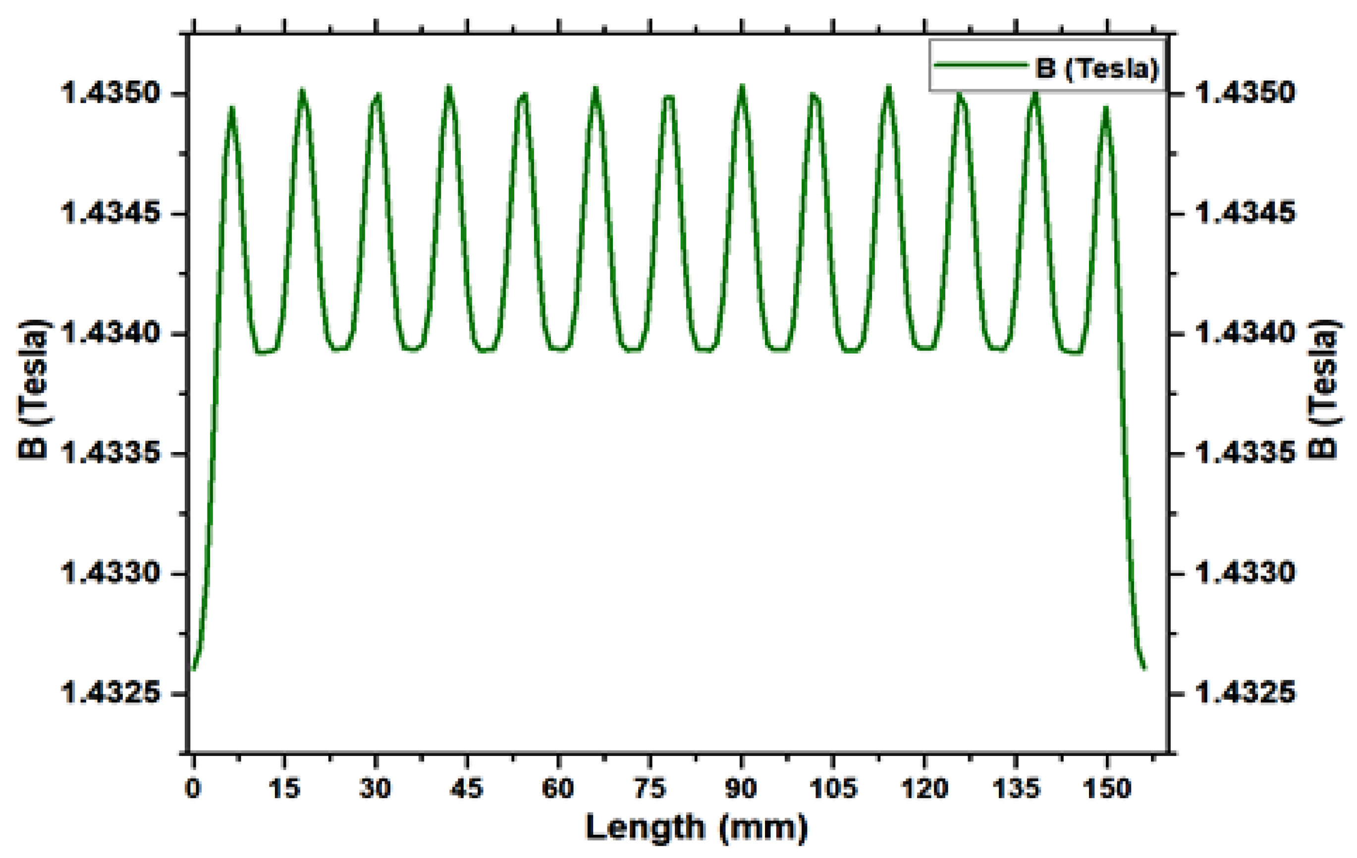
In this section, we will evaluate the self-generation system through numerical simulation with finite-element methods; to prove that the proposed solution may be successfully implemented in a self-charging device. We use FEMM Ansys software to achieve the simulation results that are depicted. The application of the permanent magnet for self-energy generation part has been explained in the previous section. Based on this assumption led to the use of the law of motion from the Maxwell equation for the overall investigation. It can charge the battery in both walking mode and shaking mode. Walking motion generates mechanical energy that may be transformed into electric energy, continually charging the battery and prolonging its useful life. The permanent magnetization is constant and aligned with the horizontal axis, which equals the oscillation direction. Figure 17 depicts the corresponding permanent magnet equilibrium position. The magnetic flux lines were computed for the magnet in the coil’s equilibrium position. Figure 18 depicts that the induced voltage is a function of the negative time derivative, the calculated variation in permanent magnetic flux as a function of time concerning the equilibrium state. The computed flux accurately reproduced the sinusoidal curve according to the above mentioned geometry. Figure 19 depicts the magnetic flux density in Tesla measured in mm as a function of the permanent magnet. The computed flux reasonably well and accurately reproduces a sinusoidal curve. The resulting voltage amplitude of 17 V, although the average absolute voltage is 15.25 V, is the lowest input value for an established rectifier circuit, which should be sufficient for the proposed harvester for an embedded smartphone self-charging application.
Figure 17. The calculated flux lines permanent shape magnet in the equilibrium position.
Figure 18. The computed difference between the permanent magnetic flux at equilibrium and the induced voltage.
Figure 19. The calculated flux density in Tesla.

4.3. RRAM Joint Model Optimization

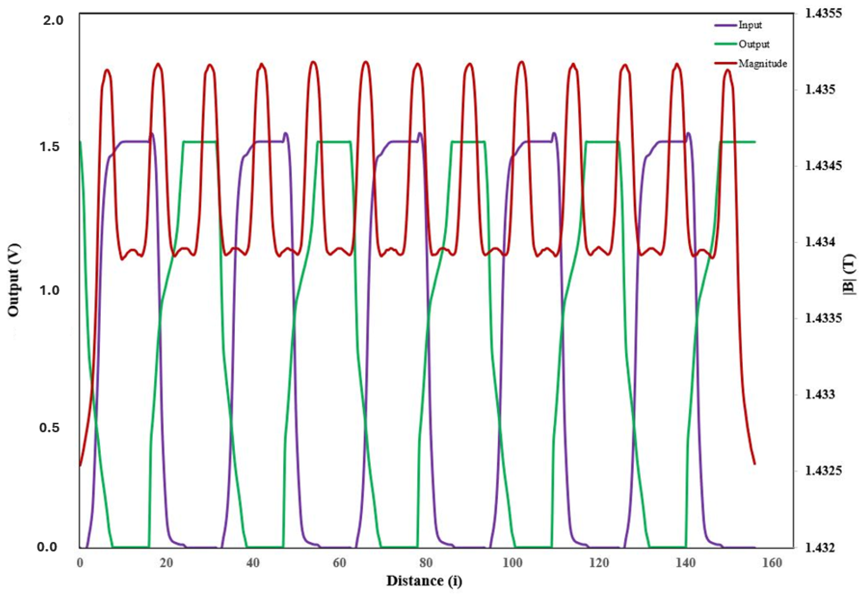
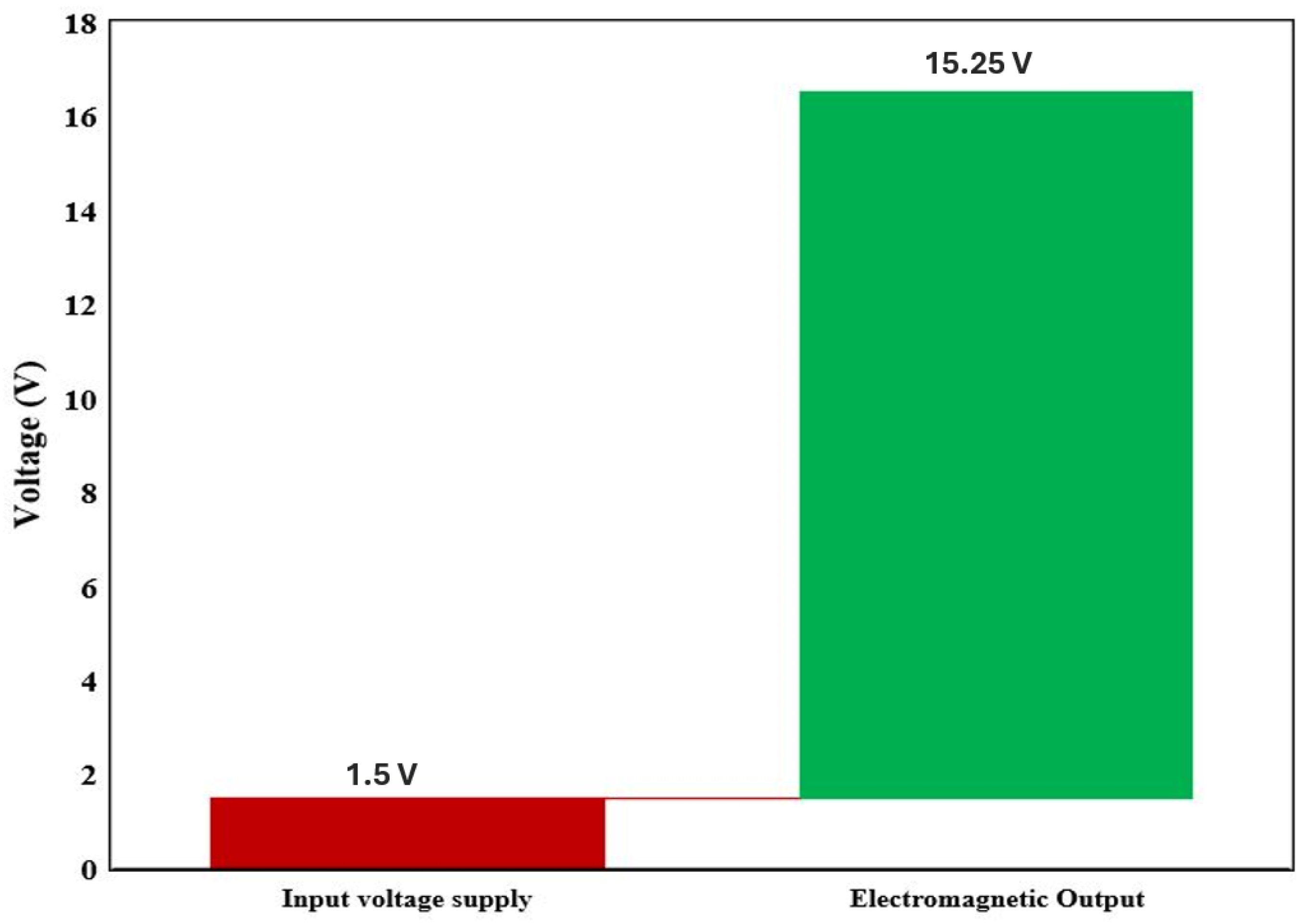
In this part, we prove the efficacy of our suggested RRAM Joint Model Optimizations, which have been programmed to generate a self-charging process. The effectiveness of the proposed joint model in converting and amplifying the input energy is demonstrated in Figure 20, which graphically supports this significant voltage amplification. The suggested approach combines self-characterization processes to improve energy harvesting and storage efficiency. Figure 21 shows the difference between the 1.5 V input voltage and the 15.25 V magnetically produced output. Although the device uses a modest input supply of 1.5 V, magnetic induction generates an impressive 15.25 V output. This output exceeds the standard operating voltage of most embedded electronic devices, which typically operates within a 12V range. Table 6 shows the measured parameters of the proposed hybrid joint model. Based on these promising results, this evaluation indicates the effectiveness of the smartphone self-charging device. We believe that this performance validates our model as a more advanced and reliable alternative in the field of smart self-charging devices.
Figure 20. A computation of the in/out effectiveness of the proposed joint model amplification.
Figure 21. Measurement comparison: input vs. magnetism generated output.
Table 6. Hybrid joint model: 1T2R input supply vs. self-charged energy generation output.

5. Conclusions

In this work, the possibility of harvesting human kinetic energy to power an embedded device has been simulated and evaluated. This simulation model is based on a developed energy generation system for integrated smartphone self-charging devices. The hybrid memristor-based self-charging system represents a promising approach for embedded smartphone energy solutions. It has a potential to drastically minimize the need for frequent charging and lead to a more energy-efficient and sustainable mobile technology ecosystem. The concept of using an RRAM device within an optimized cylinder-shaped permanent magnet in a CMOS memristor-based cell has been proposed. We employ a self-generation technique based on magnetic induction caused by the oscillation of a permanent magnet in a coil, and we propose a permanent magnet in the shape of a cylinder. This same approach was used in [19,20,22,23]. The design building block was simulated with the CMOS (130 nm) technology. To determine the induced voltage within the parameters of the finite-element method. Our research results show that we can use the significant thermoelectric voltage at the nanoscale to produce very intense transit-self-charging embedded devices. This approach, which incorporates energy harvesting and intelligent power management, can significantly prolong battery life and improve the sustainability of smartphone technology for self-charging device applications. We have also elaborated on how combining multiples of these blocks can form a self-charging device. The ultimate result might be an inventive transformation based on self-charging cell phones in the electronics sector. Finally, this breakthrough could revolutionize how smartphones manage energy, resulting in more autonomous and ecologically friendly devices. Future research will focus on further optimizing the architecture, addressing scalability difficulties, and investigating the integration of other developing energy sources for healthcare/serval different applications.

Author Contributions

Conceptualization, A.V. (Abhinav Vishwakarma) and S.K.V.; Methodology, A.V. (Abhinav Vishwakarma) and A.V. (Anubhav Vishwakarma); Software, cadence 130 nm and Open source FEMM software A.V. (Abhinav Vishwakarma) and A.V. (Anubhav Vishwakarma); Validation, A.V. (Abhinav Vishwakarma) and A.V. (Anubhav Vishwakarma); Formal analysis, A.V. (Anubhav Vishwakarma) and M.H.; Resources, M.H.; Writing—original draft, A.V. (Abhinav Vishwakarma); Writing—review & editing, M.K., S.K.V. and M.H.; Supervision, S.K.V. and M.H. All authors have read and agreed to the published version of the manuscript.

Funding

This research received no external funding.

Data Availability Statement

The original contributions presented in the study are included in the article, further inquiries can be directed to the corresponding author.

Acknowledgments

The authors would like to thank the Brandenburgische Technische Universitat Cottbus-Senftenberg, Germany, for providing the necessary Research Facilities. We grateful to the Jožef Stefan Institute, Ljubljana, Slovenia, for offering facilities and resources for this research. Their support facilitated the smooth execution of the study.

Conflicts of Interest

The authors declare no conflicts of interest regarding this article.

References

  1. Bazzi, H.; Harb, A.; Aziza, H.; Moreau, M.; Kassem, A. RRAM-based non-volatile SRAM cell architectures for ultra-low-power applications. Analog. Integr. Circuits Signal Process. 2021, 106, 351–361. [Google Scholar] [CrossRef]
  2. Hamdioui, S.; Aziza, H.; Sirakoulis, G.C. Memristor-based memories: Technology, design, and test. In Proceedings of the 9th IEEE International Conference on Design & Technology of Integrated Systems in Nanoscale Era (DTIS), Santorini, Greece, 6–8 May 2014; pp. 1–7. [Google Scholar]
  3. Akerman, J. Applied physics: Toward a universal memory. Science 2005, 308, 508–510. [Google Scholar] [CrossRef]
  4. Waser, R.; Aono, M. Nanoionics-based resistive switching memories. Nature 2007, 6, 833–840. [Google Scholar] [CrossRef]
  5. Bazzi, H.; Harb, A.; Aziza, H.; Moreau, M. Non-volatile SRAM memory cells based on ReRAM technology. SN Appl. Sci. 2020, 2, 1485. [Google Scholar] [CrossRef]
  6. Li, Q.; Liu, S. Adaptive Modified Function Projective Lag Synchronization of Memristor-Based Five-Order Chaotic Circuit Systems. Adv. Math. Phys. 2017, 2017, 1843179. [Google Scholar] [CrossRef]
  7. MacVittie, K.; Katz, E. Self-powered electrochemical memristor based on a biofuel cell-towards memristors integrated with biocomputing systems. Chem. Commun. 2014, 50, 4816–4819. [Google Scholar] [CrossRef]
  8. Yang, X.; Xiong, Z.; Chen, Y.; Ren, Y.; Zhou, L.; Li, H.; Zhou, Y.; Pan, F.; Han, S. A self-powered artificial retina perception system for image preprocessing based on photovoltaic devices and memristive arrays. Nano Energy 2020, 78, 105246. [Google Scholar] [CrossRef]
  9. Shi, J.; Wang, Z.; Tao, Y.; Xu, H.; Zhao, X.; Lin, Y.; Liu, Y. Self-Powered Memristive Systems for Storage and Neuromorphic Computing. Front. Neurosci. 2021, 15, 662457. [Google Scholar] [CrossRef]
  10. Sun, B.; Zhou, G.; Xu, K.; Yu, Q.; Duan, S. Self-Powered Memory Systems. ACS Mater. Lett. 2020, 2, 1669–1690. [Google Scholar] [CrossRef]
  11. Lee, B.; Cho, H.; Park, K.T.; Kim, J.; Park, M.; Kim, H.; Hong, Y.; Chung, S. High-performance compliant thermoelectric generators with magnetically self-assembled soft heat conductors for self-powered wearable electronics. Nat. Commun. 2020, 11, 5948. [Google Scholar] [CrossRef] [PubMed]
  12. Yin, J.; Li, X.; Yu, J.; Zhang, Z.; Zhou, J.; Guo, W. Generating electricity by moving a droplet of ionic liquid along graphene. Nat. Nanotechnol. 2014, 9, 378–383. [Google Scholar] [CrossRef] [PubMed]
  13. Yoon, J.H.; Wang, Z.; Kim, K.M.; Wu, H.; Ravichandran, V.; Xia, Q.; Hwang, C.S.; Yang, J.J. An artificial nociceptor based on a diffusive memristor. Nat. Commun. 2018, 9, 417. [Google Scholar] [CrossRef]
  14. Zhang, J.; Yang, C.; Liang, H.; Cao, Z.; Duan, X.; Ya, W.; Zhao, Y.; Sun, B. Memristor-based electronic devices towards biomedical applications. J. Mater. Chem. 2024, 12, 50–59. [Google Scholar] [CrossRef]
  15. Shearwood, C.; Yates, R.B. Development of an electromagnetic micro-generator. Electron. Lett. 1997, 33, 1883–1884. [Google Scholar] [CrossRef]
  16. Amirtharajah, R.; Chandrakasan, A.P. Self-powered signal processing using vibration-based power generation. IEEE J. Solid-State Circuits 1998, 33, 687–695. [Google Scholar] [CrossRef]
  17. Ching, N.N.; Wong, H.Y.; Li, W.J.; Leong, P.H.; Wen, Z. A laser-micromachined multi-modal resonating power transducer for wireless sensing systems. Sens. Actuators A Phys. 2002, 97–98, 685–690. [Google Scholar] [CrossRef]
  18. Choi, S.; Yang, J.; Wang, G. Emerging Memristive Artificial Synapses and Neurons for Energy-Efficient Neuromorphic Computing. Adv. Mater. 2020, 32, 2004659. [Google Scholar] [CrossRef] [PubMed]
  19. Vishwakarma, A.; Komelj, M. Design of a Smart Phone Self-Charging Device Based on Permanent Magnets. Adv. Transdiscipl. Eng. 2022, 27, 507–513. [Google Scholar]
  20. Vishwakarma, A.; Komelj, M. A permanent magnet-based design for a smartphone self-charger. Mater. Today Proc. 2022, 65 Pt 8, 3642–3645. [Google Scholar] [CrossRef]
  21. Vishwakarma, A.; Komelj, M. Optimum Design of a Permanent-Magnet-Based Self-Charging Device for a Smartphone. MatTech Mater. Technol. 2023, 57, 627–630. [Google Scholar] [CrossRef]
  22. Vishwakarma, A.; Ampadu, K.O.; Huebner, M.; Vishvakarma, S.; Reichenbach, M. Memristor-Based CMOS Hybrid Circuit Design and Analysis. Procedia Comput. Sci. 2023, 218, 563–573. [Google Scholar] [CrossRef]
  23. Abdoli, B.; Amirsoleimani, A.; Shamsi, J.; Mohammadi, K.; Ahmadi, A. A novel CMOS-memristor based inverter circuit design. In Proceedings of the 22nd Iranian Conference on Electrical Engineering (ICEE), Tehran, Iran, 20–22 May 2014; pp. 276–371. [Google Scholar]
  24. Sharma, G.; Bhargava, L. CMOS-memristor inverter circuit design and analysis using Cadence Virtuoso. In Proceedings of the International Conference on Recent Advances and Innovations in Engineering (ICRAIE), Jaipur, India, 23–25 December 2016; pp. 1–5. [Google Scholar] [CrossRef]
  25. Khalid, M. Review on Various Memristor Models, Characteristics, Potential Applications, and Future Works. Trans. Electr. Electron. Mater. 2019, 20, 289–298. [Google Scholar] [CrossRef]
  26. Sanca, G.A.; Di Francesco, F.; Caroli, N.; Garcia-Inza, M.; Golmar, F. Design of a Simple Readout Circuit for Resistive Switching Memristors Based on CMOS Inverters. In Proceedings of the IEEE 4th International Forum on Research and Technology for Society and Industry (RTSI), Palermo, Italy, 24–26 August 2018; pp. 1–6. [Google Scholar] [CrossRef]
  27. Biolek, Z.; Biolek, D.; Biolkova, V. SPICE model of memristor with nonlinear dopant drift. Radioengineering 2009, 18, 210–214. [Google Scholar]
  28. Strukov, D.B.; Snider, G.S.; Stewart, D.R.; Williams, R.S. The missing memristor found. Nature 2008, 453, 80–83. [Google Scholar] [CrossRef]
  29. Vishwakarma, A.; Fritscher, M.; Hagelauer, A.; Reichenbach, M. An RRAM-based building block for reprogrammable non-uniform sampling ADCs. it-Inf. Technol. 2023, 65, 39–51. [Google Scholar] [CrossRef]
  30. Zhang, X.; Cao, Y.; Peng, L.; Li, J.; Ahmad, N.; Yu, S. Mobile Charging as a Service: A Reservation-Based Approach. IEEE Trans. Autom. Sci. Eng. 2020, 17, 1976–1988. [Google Scholar] [CrossRef]
  31. Wu, C.; Kim, T.W.; Park, B.; Sung, S.; Shao, J.; Zhang, C.; Wang, Z.L. Self-powered tactile sensor with learning and memory. ACS Nano 2019, 14, 1390–1398. [Google Scholar] [CrossRef]
  32. Nekui, O.D.; Wang, W.; Liu, C.; Wang, Z.; Ding, B. IoT-Based Heartbeat Rate-Monitoring Device Powered by Harvested Kinetic Energy. Sensors 2024, 24, 4249. [Google Scholar] [CrossRef]
  33. Saha, C.R.; O’donnell, T.; Wang, N.; McCloskey, P. Electromagnetic generator for harvesting energy from human motion. Sens. Actuators A Phys. 2008, 147, 248–253. [Google Scholar] [CrossRef]
  34. Park, S.; Kim, B.; Kim, S.; Lee, K.; Kim, J. Electric generator embedded in cellular phone for self-recharge. J. Vibroengineering 2014, 16, 3797–3806. [Google Scholar]
  35. Liu, Y.; Yang, W.; Yan, Y.; Wu, X.; Wang, X.; Zhou, Y.; Hu, Y.; Chen, H.; Guo, T. Self-powered high-sensitivity sensory memory actuated by triboelectric sensory receptor for real-time neuromorphic computing. Nano Energy 2020, 75, 104930. [Google Scholar] [CrossRef]
  36. Dastgeer, G.; Nisar, S.; Rasheed, A.; Akbar, K.; Chavan, V.D.; Kim, D.; Wabaidur, S.M.; Zulfiqar, M.W.; Eom, J. Atomically engineered, high-speed non-volatile flash memory device exhibiting multibit data storage operations. Nano Energy 2024, 119, 109106. [Google Scholar] [CrossRef]
  37. Dastgeer, G.; Nisar, S.; Zulfiqar, M.W.; Eom, J.; Imran, M.; Akbar, K. A review on recent progress and challenges in high-efficiency perovskite solar cells. Nano Energy 2024, 132, 110401. [Google Scholar] [CrossRef]
  38. Jiang, Z.; Wu, Y.; Yu, S.; Yang, L.; Song, K.; Karim, Z.; Wong, H.S.P. A compact model for metal oxide resistive random access memory with experiment verification. IEEE Trans. Electron Devices 2016, 63, 1884–1892. [Google Scholar] [CrossRef]
  39. Reuben, J.; Fey, D.; Wenger, C. A modeling methodology for resistive RAM based on the Stanford PKU model with extended multilevel capability. IEEE Trans. Nanotechnol. 2019, 18, 647–656. [Google Scholar] [CrossRef]
  40. Majumdar, S.; Kingra, S.K.; Suri, M.; Tikyani, M. Hybrid CMOS-OxRAM-based 4T-2R NVSRAM with efficient programming scheme. In Proceedings of the 16th Non-Volatile Memory Technology Symposium (NVMTS), Pittsburgh, PA, USA, 17–19 October 2016; pp. 1–4. [Google Scholar] [CrossRef]
  41. Janniekode, U.M.; Somineni, R.P.; Khalaf, O.I.; Itani, M.M.; Chinna Babu, J.; Abdulsahib, G.M. A Symmetric Novel 8T3R Non-Volatile SRAM Cell for Embedded Applications. Symmetry 2022, 14, 768. [Google Scholar] [CrossRef]
  42. Yadav, M.; Handa, P. Design and Comparative Power Analysis of Conventional 6T SRAM with 7T2M nv-SRAM at 180 nm Technology. Adv. Intell. Syst. Comput. 2022, 1373, 373–383. [Google Scholar] [CrossRef]
  43. Pérez-Bosch Quesada, E.; Romero-Zaliz, R.; Pérez, E.; Kalishettyhalli Mahadevaiah, M.; Reuben, J.; Schubert, M.A.; Jiménez-Molinos, F.; Roldán, J.B.; Wenger, C. Toward Reliable Compact Modeling of Multilevel 1T-1R RRAM Devices for Neuromorphic Systems. Electronics 2021, 10, 645. [Google Scholar] [CrossRef]
Disclaimer/Publisher’s Note: The statements, opinions and data contained in all publications are solely those of the individual author(s) and contributor(s) and not of MDPI and/or the editor(s). MDPI and/or the editor(s) disclaim responsibility for any injury to people or property resulting from any ideas, methods, instructions or products referred to in the content.

Article Metrics

Citations

Article Access Statistics

Multiple requests from the same IP address are counted as one view.