
A Time-to-Digital Converter for Low-Power Consumption Single Slope Analog-to-Digital Converters in a High-Speed CMOS Image Sensor

Abstract
1. Introduction
2. Proposed Structure
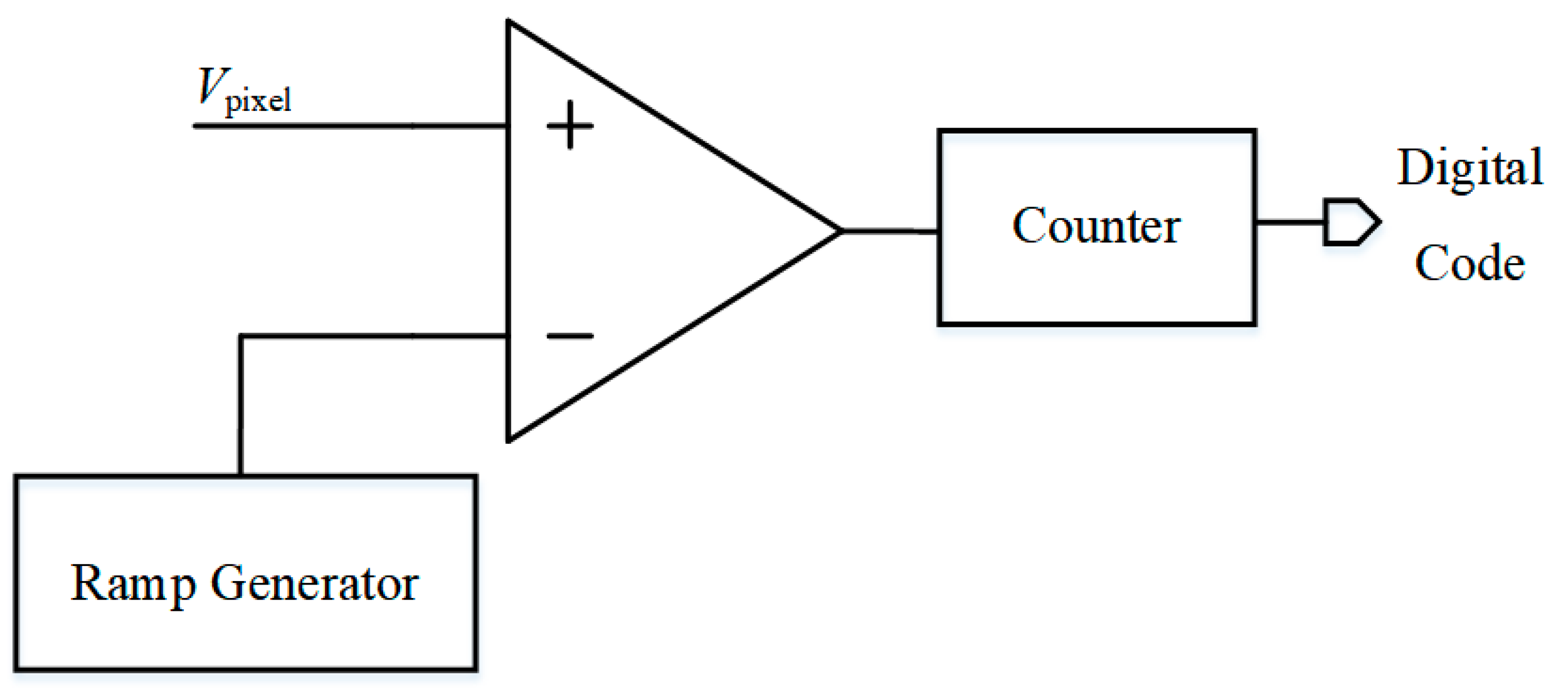
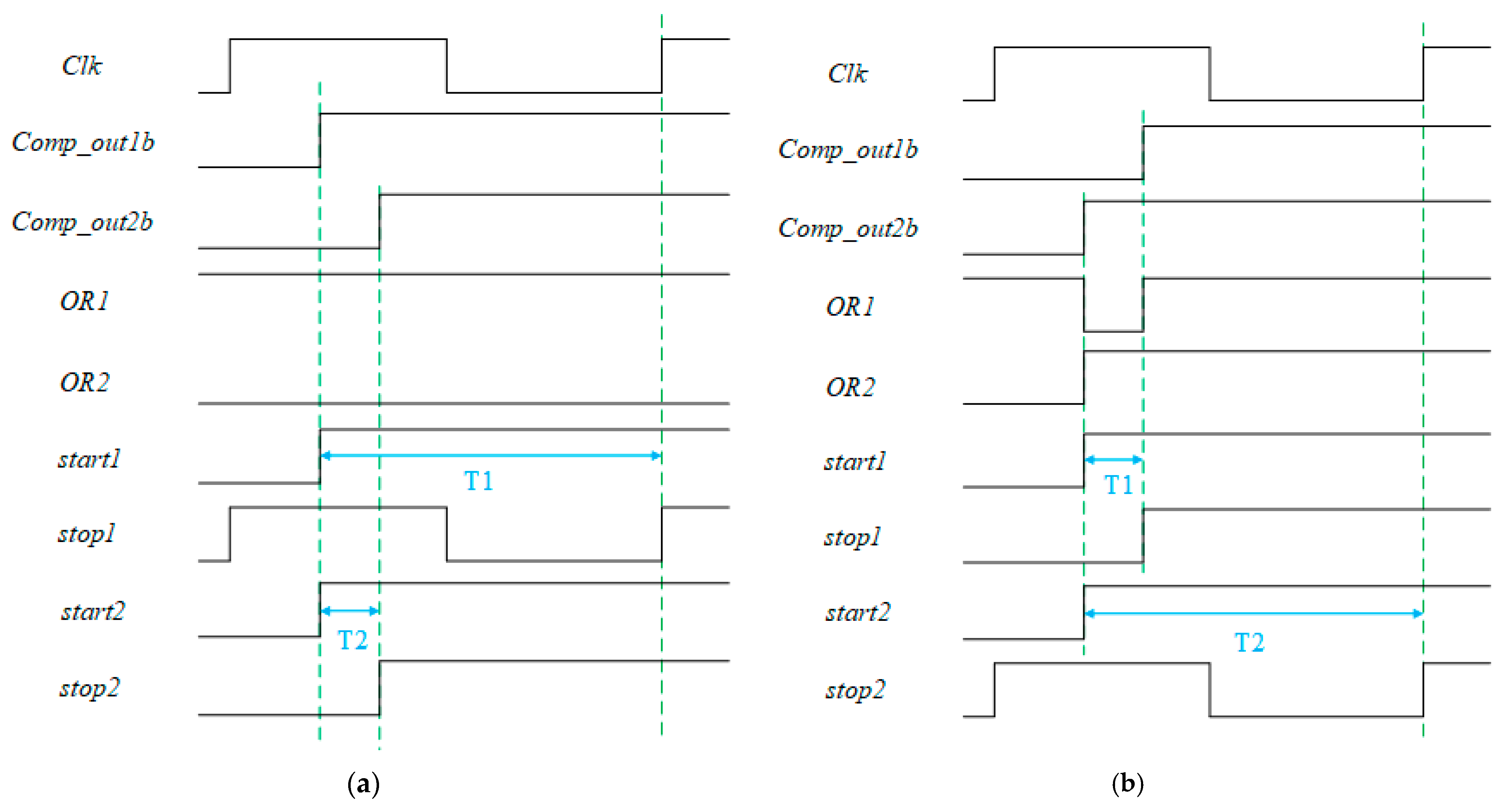
2.1. Traditional Structure
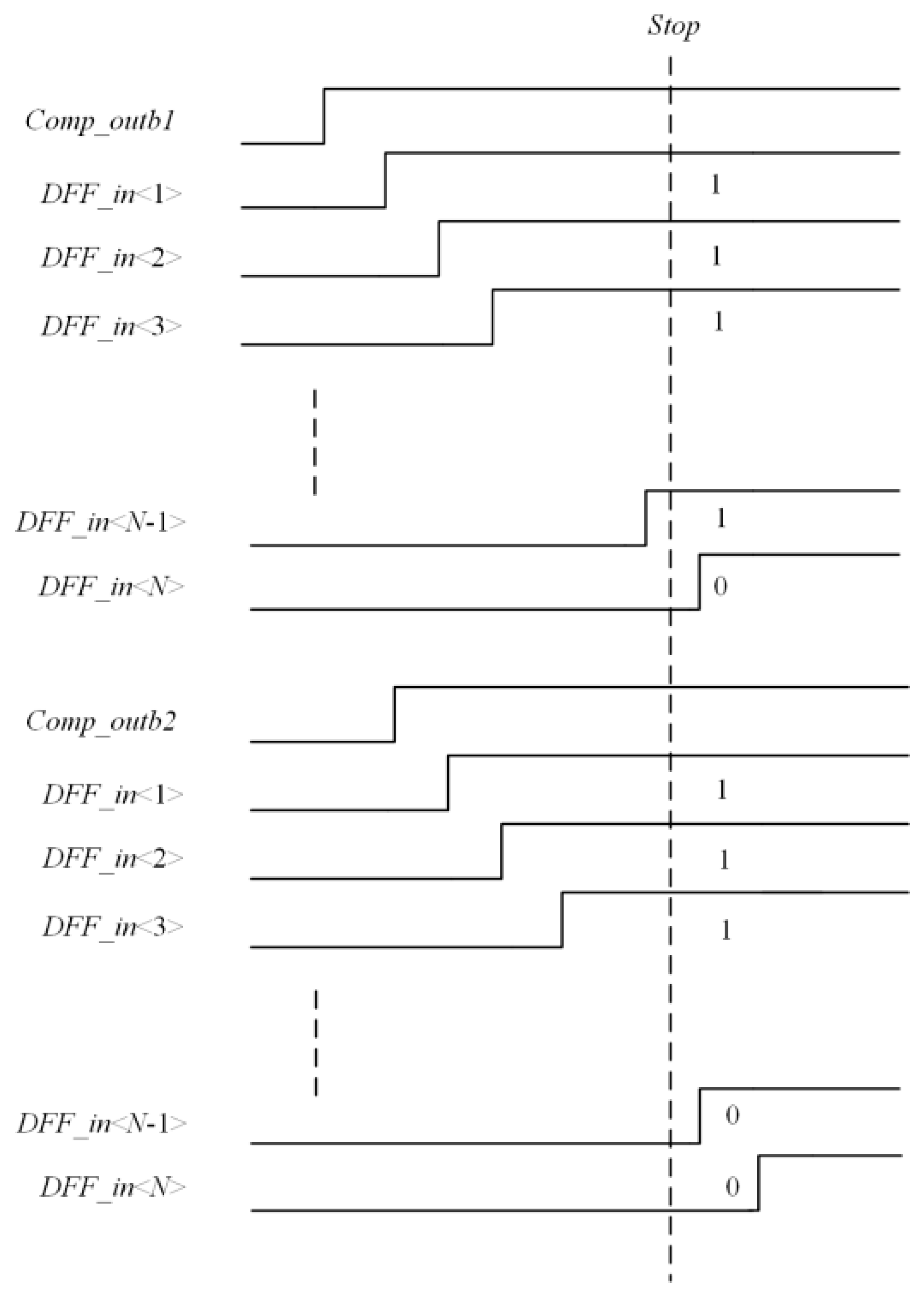
2.2. Power Consumption Analysis of TDC
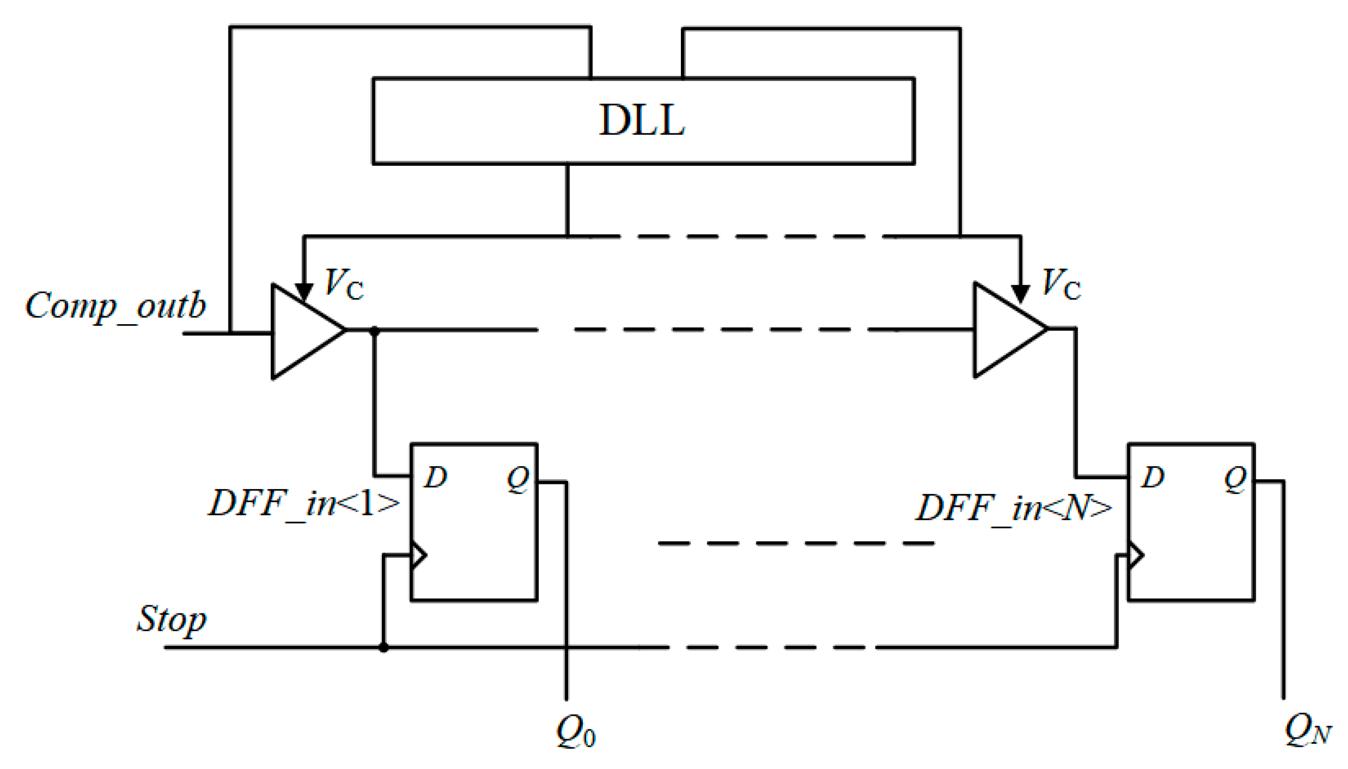
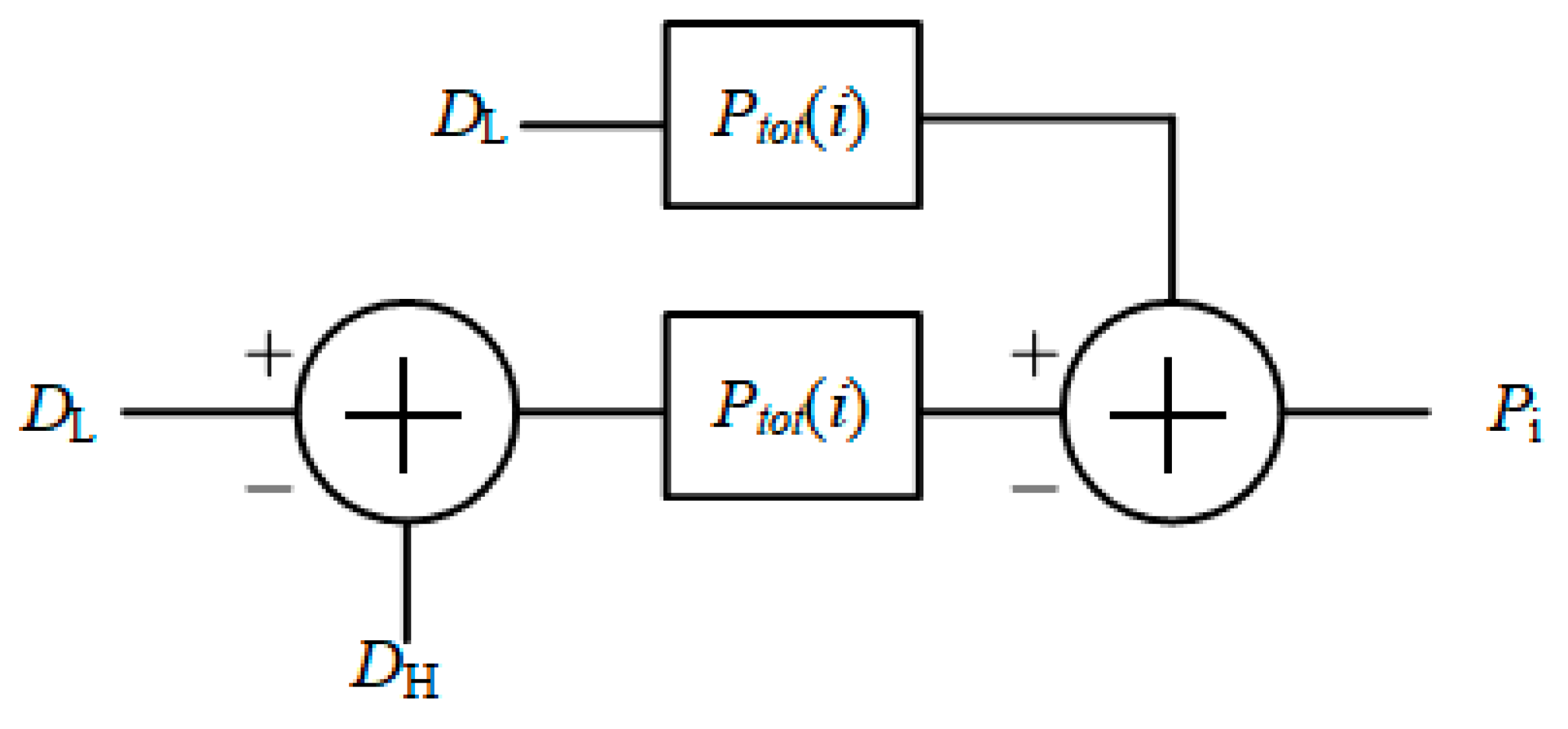
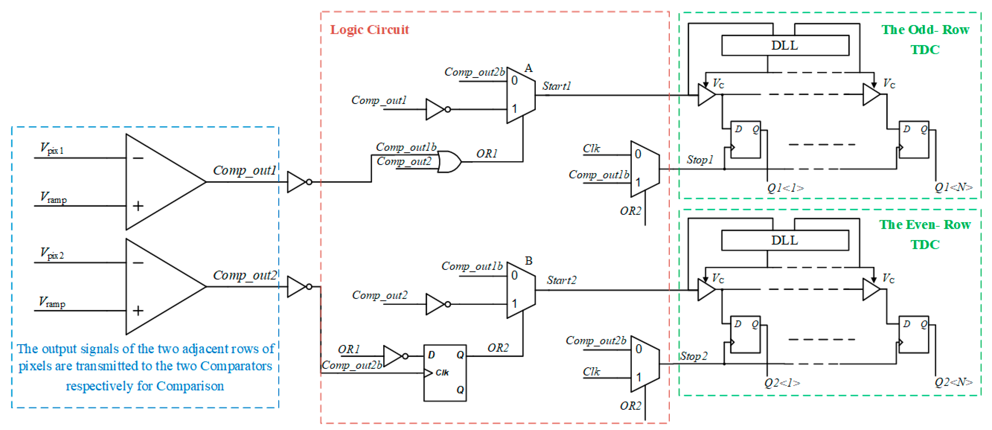
2.3. Proposed TDC
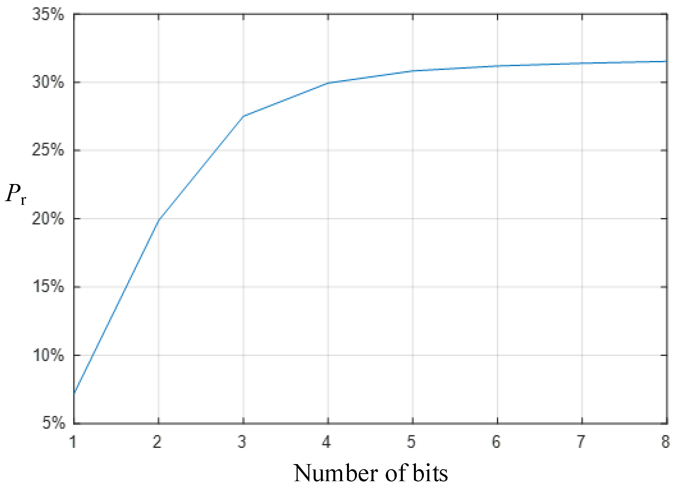
3. Modeling Analysis
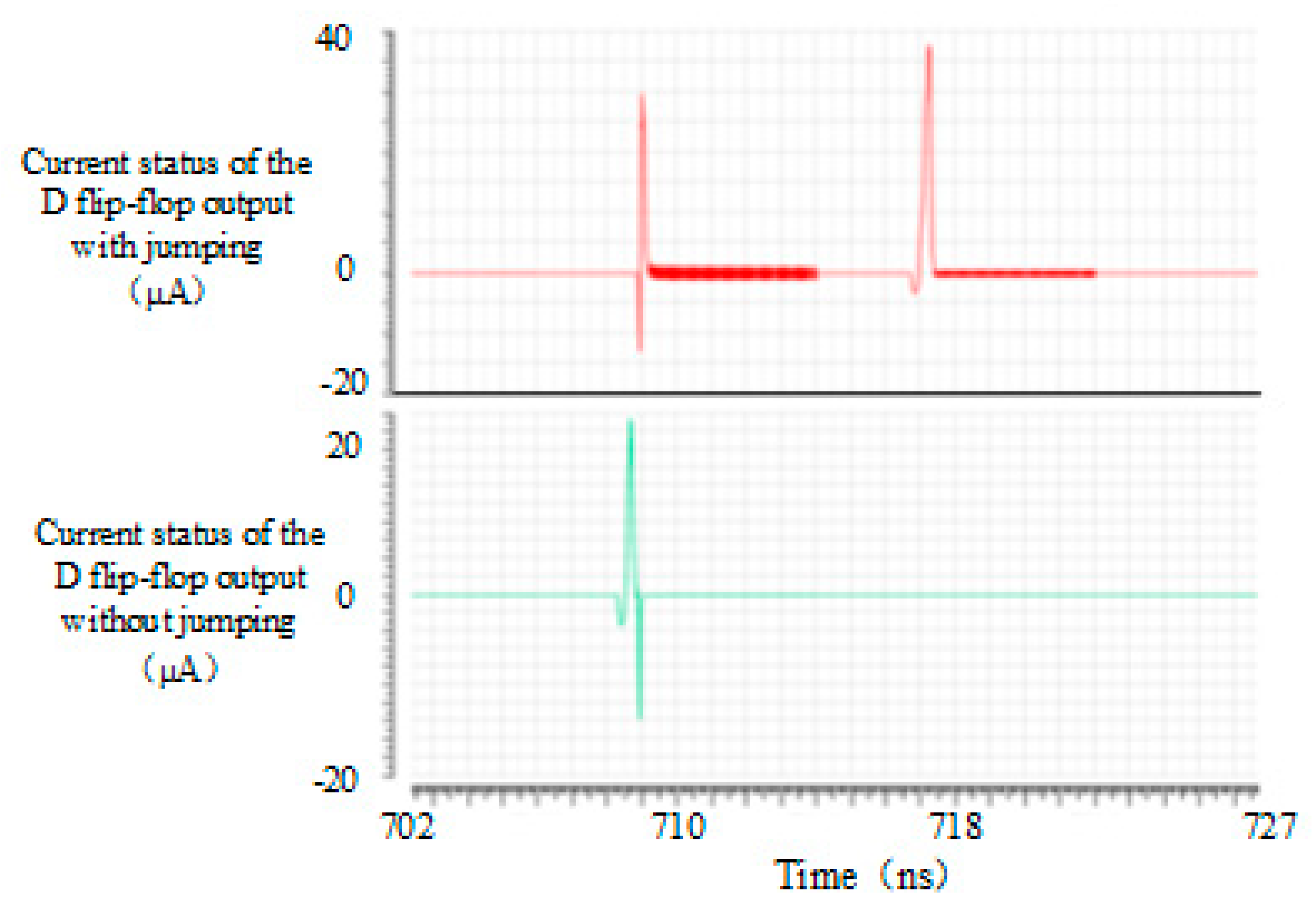
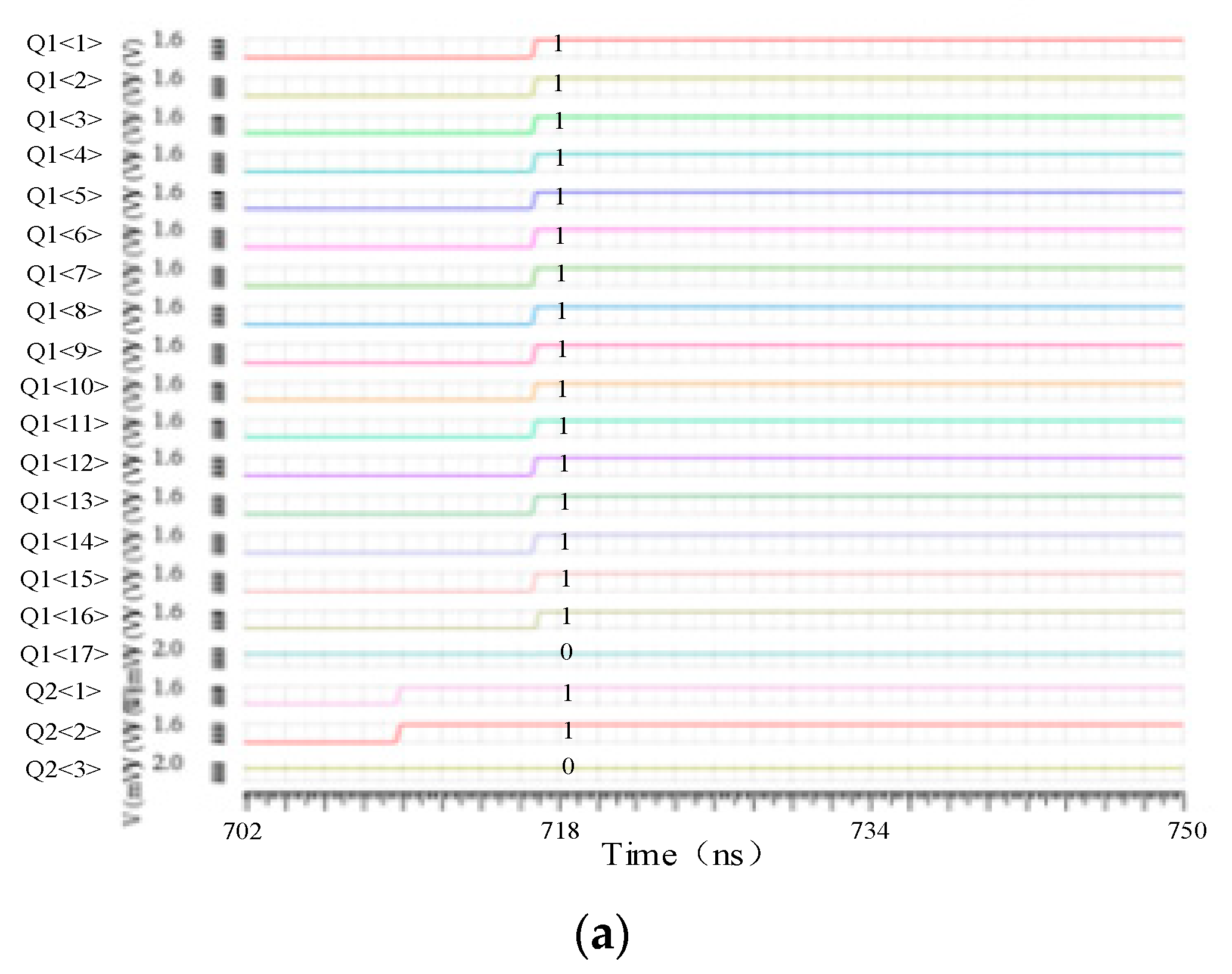
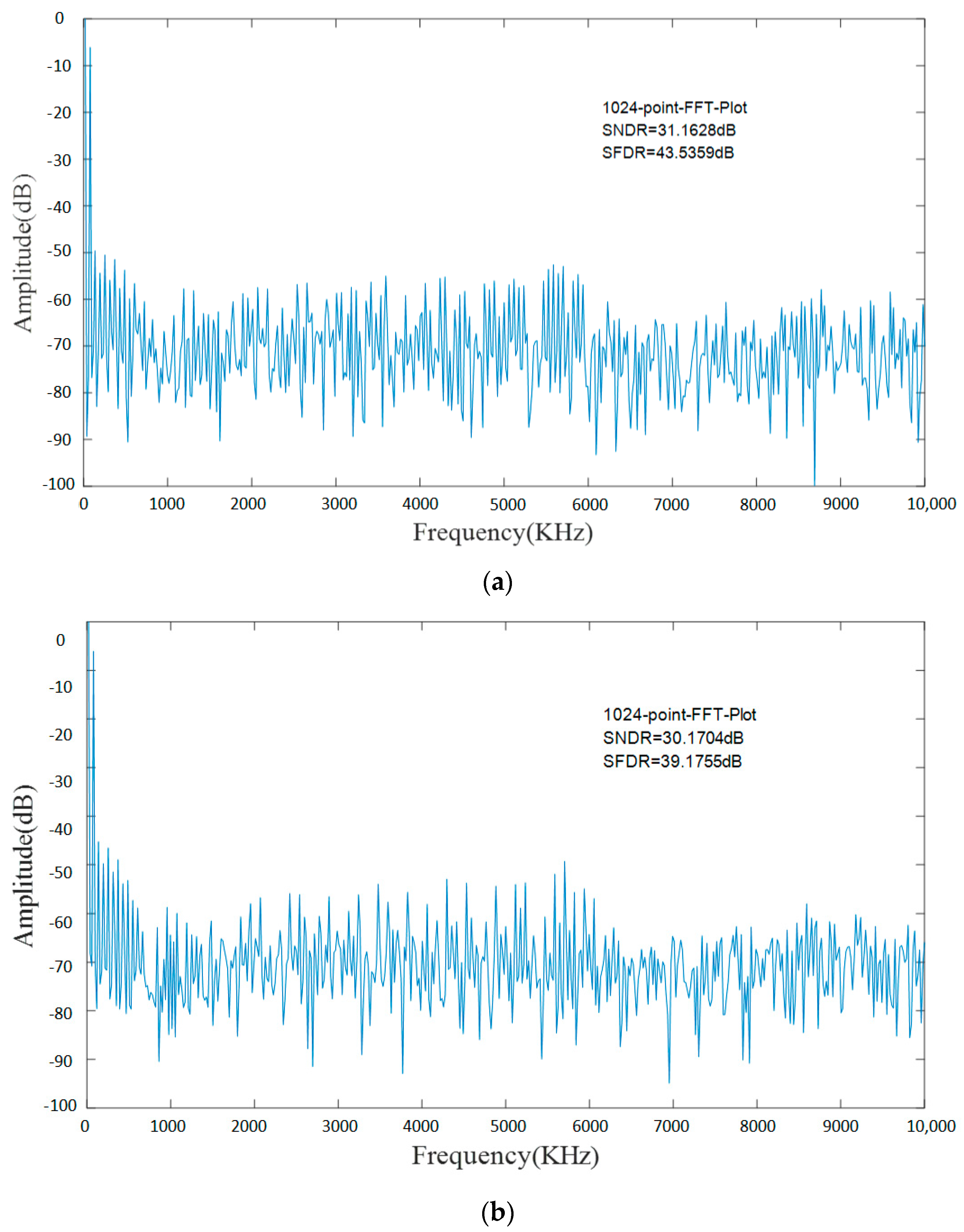
4. Simulation Results
5. Conclusions
Author Contributions
Funding
Data Availability Statement
Conflicts of Interest
References
- Gao, J.; Yan, N.; Nie, K.; Gao, Z.; Xu, J. A 2.44 μs row conversion time 12-bit high-speed differential single-slope ADC with TDC applied to CMOS image sensor. Microelectron. J. 2022, 102, 105322. [Google Scholar] [CrossRef]
- Levski, D.; Wäny, M.; Choubey, B. A 1- us Ramp Time 12-bit Column-Parallel Flash TDC-Interpolated Single-Slope ADC with Digital Delay-Element Calibration. IEEE Trans. Circuits Syst. I Regul. Pap. 2019, 66, 54–67. [Google Scholar] [CrossRef]
- Wang, Y.; Guo, Z.; Guo, Y.; Xu, R.; Wang, B.; Liu, S. High Speed Column Level ADC Design with TDC Technology for CMOS Image Sensor. In Proceedings of the 2023 6th International Conference on Electronics Technology (ICET), Chengdu, China, 12–15 May 2023; pp. 180–184. [Google Scholar]
- Abdelmejeed, M.; Guindi, R.; Abdel-Moneum, M. A novel 10-Bit high-throughput two-stage TDC with reduced power and improved linearity. In Proceedings of the 2013 4th Annual International Conference on Energy Aware Computing Systems and Applications (ICEAC), Istanbul, Turkey, 16–18 December 2013; pp. 50–54. [Google Scholar]
- Lu, P.; Wu, Y. A 90 nm CMOS digital PLL based on vernier-gated-ring-oscillator time-to-digital converter. In Proceedings of the IEEE International Symposium on Circuits and Systems (ISCAS), Seoul, Republic of Korea, 20–23 May 2012; pp. 2593–2596. [Google Scholar]
- Liu, J.; Hassanpourghadi, M.; Chen, M. A 10GS/s 8b 25fJ/c-s 2850 μm2 two-step time-domain ADC using delay-tracking pipelined-SAR TDC with 500 fs time step in 14 nm CMOS technology. In Proceedings of the International Solid-State Circuits Conference (ISSCC), San Francisco, CA, USA, 18–22 February 2022; pp. 160–162. [Google Scholar]
- Yi, X.; Liang, Z.; Boon, C.; Feng, G.; Meng, F.; Yang, K. An inverted ring oscillator noise-shaping time-to-digital converter with in-band noise reduction and coherent noise cancellation. IEEE Trans. Circuits Syst. I Regul. Pap. 2020, 67, 686–698. [Google Scholar] [CrossRef]
- Teh, J.S.; Siek, L.A. 12-bit branching time-to-digital converter with power saving features and digital based resolution tuning for PVT variations. Analog. Integr. Circuits Signal Process. 2020, 105, 57–71. [Google Scholar] [CrossRef]
- Tangudu, J.; Gunturi, S.; Jalan, S.; Janardhanan, J.; Ganesan, R.; Sahu, D.; Waheed, K.; Wallberg, J.; Staszewski, R.B. Quantization noise improvement of Time to Digital Converter (TDC) for ADPLL. In Proceedings of the 2009 IEEE International Symposium on Circuits and Systems, Chengdu, China, 28–29 April 2009. [Google Scholar]
- Zhang, F.; Tang, L.; Zhang, Y.; Tang, X.; Wang, Z. A Low-Power Two-Step Time-to-Digital Conversion in 28 nm CMOS. In Proceedings of the 2022 7th International Conference on Integrated Circuits and Microsystems (ICICM), Xi’an, China, 28–31 October 2022; pp. 570–573. [Google Scholar]
- Han, S.H.; Kim, B.; Park, S.; Park, Y.; Chun, J.H.; Choi, J.; Kim, S.J. A 100 × 80 CMOS Flash LiDAR Sensor with 0.0011 mm2 In-Pixel Histogramming TDC Based on Analog Counter and Self-Calibrated Single-Slope ADC. In Proceedings of the 2022 IEEE Symposium on VLSI Technology and Circuits (VLSI Technology and Circuits), Honolulu, HI, USA, 12–17 June 2022; pp. 82–83. [Google Scholar]
- Rostami, M.S.; Saberi, M.; Maymandi-Nejad, M.; Sawan, M. A Low-Power Time-to-Digital Converter for Sensor Interface Circuits. IEEE Trans. Circuits Syst. II Express Briefs 2020, 67, 2853–2857. [Google Scholar] [CrossRef]
- Pedram, M. Power Minimization in IC Design: Principles and Applications. ACM Trans. Des. Autom. 1996, 1, 3–56. [Google Scholar] [CrossRef]
- Wang, G.; Chen, Q.; Xu, J.; Nie, K. 2 μs row time 12-bit column-parallel single slope ADC for high-speed CMOS image sensor. Microelectron. J. 2023, 135, 105768. [Google Scholar] [CrossRef]
- Molaei, H.; Hajsadeghi, K. A 5.3-ps, 8-b Time to Digital Converter Using a New Gain-Reconfigurable Time Amplifier. IEEE Trans. Circuits Syst. 2019, 66, 352–356. [Google Scholar] [CrossRef]


| [12] | [14] | [15] | This Work | |
|---|---|---|---|---|
| CMOS process | 65 nm | 0.11 μm | 0.18 μm | 0.11 μm |
| Number of bits | 8 | 12 | 8 | 5 |
| Sampling rate (MS/s) | 0.2 | 0.5 | 30 | 20 |
| Power (μW) | 10 | 187 | 1100 | 60–93 |
| ENOB (bits) | 7.52 | 10.68 | 6.07 | 4.72 |
| FOM * (fJ/step) | 275.0 | 182.6 | 540.0 | 104.7–162.3 |
Disclaimer/Publisher’s Note: The statements, opinions and data contained in all publications are solely those of the individual author(s) and contributor(s) and not of MDPI and/or the editor(s). MDPI and/or the editor(s) disclaim responsibility for any injury to people or property resulting from any ideas, methods, instructions or products referred to in the content. |
© 2024 by the authors. Licensee MDPI, Basel, Switzerland. This article is an open access article distributed under the terms and conditions of the Creative Commons Attribution (CC BY) license (https://creativecommons.org/licenses/by/4.0/).
Share and Cite
Li, Z.; Gao, Z. A Time-to-Digital Converter for Low-Power Consumption Single Slope Analog-to-Digital Converters in a High-Speed CMOS Image Sensor. Micromachines 2024, 15, 578. https://doi.org/10.3390/mi15050578
Li Z, Gao Z. A Time-to-Digital Converter for Low-Power Consumption Single Slope Analog-to-Digital Converters in a High-Speed CMOS Image Sensor. Micromachines. 2024; 15(5):578. https://doi.org/10.3390/mi15050578
Chicago/Turabian StyleLi, Ziyi, and Zhiyuan Gao. 2024. "A Time-to-Digital Converter for Low-Power Consumption Single Slope Analog-to-Digital Converters in a High-Speed CMOS Image Sensor" Micromachines 15, no. 5: 578. https://doi.org/10.3390/mi15050578
APA StyleLi, Z., & Gao, Z. (2024). A Time-to-Digital Converter for Low-Power Consumption Single Slope Analog-to-Digital Converters in a High-Speed CMOS Image Sensor. Micromachines, 15(5), 578. https://doi.org/10.3390/mi15050578