
Magnetic-Field-Assisted Electric-Field-Induced Domain Switching of a Magnetic Single Domain in a Multiferroic/Magnetoelectric Ni Nanochevron/[Pb(Mg1/3Nb2/3)O3]0.68–[PbTiO3]0.32 (PMN–PT) Layered Structure


Abstract
:1. Introduction
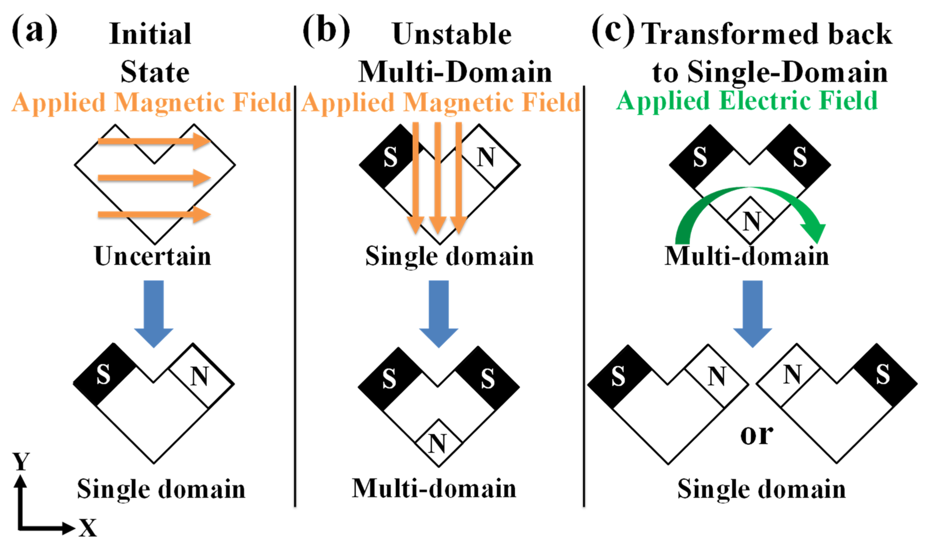
2. Design
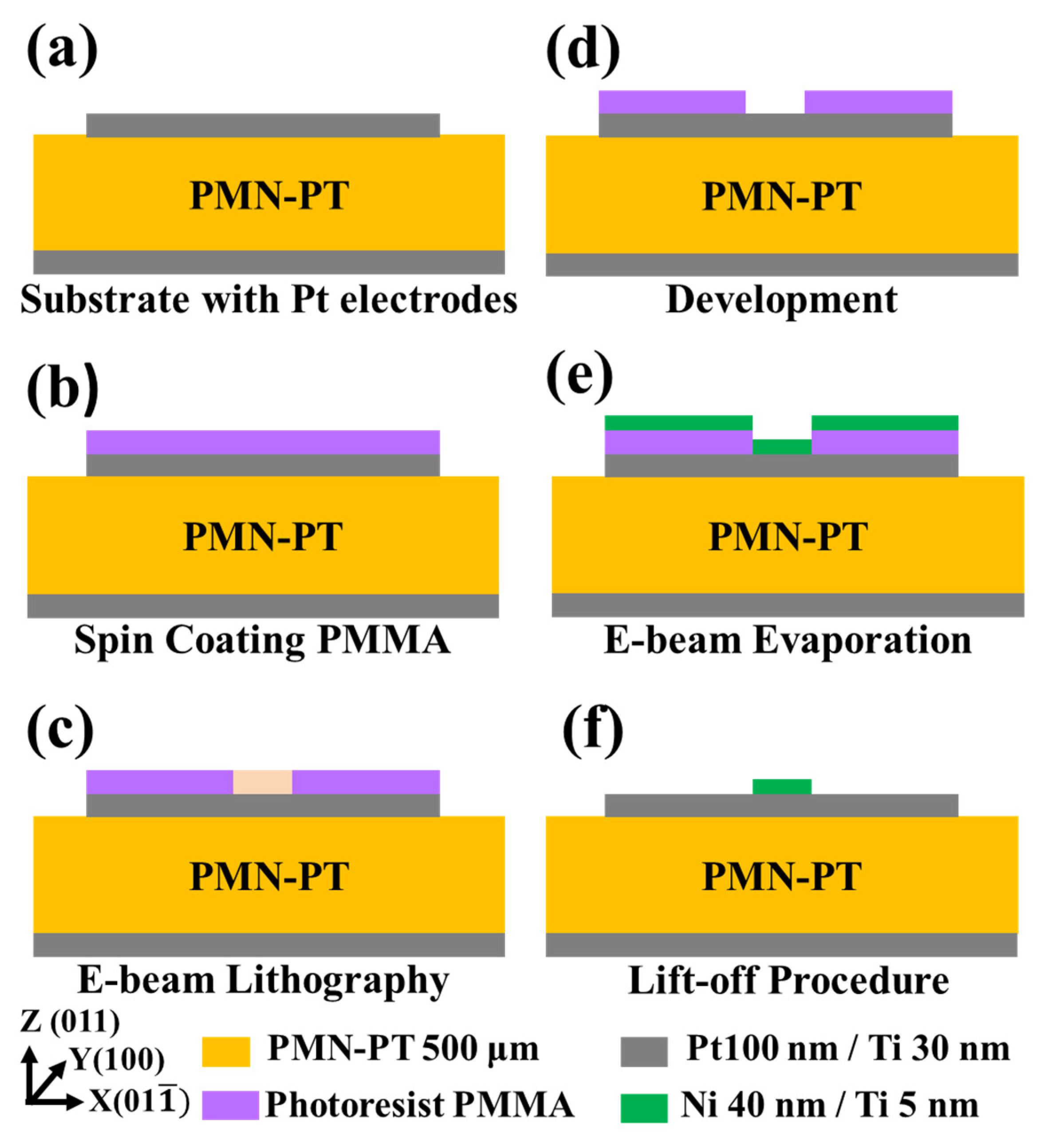
3. Fabrication
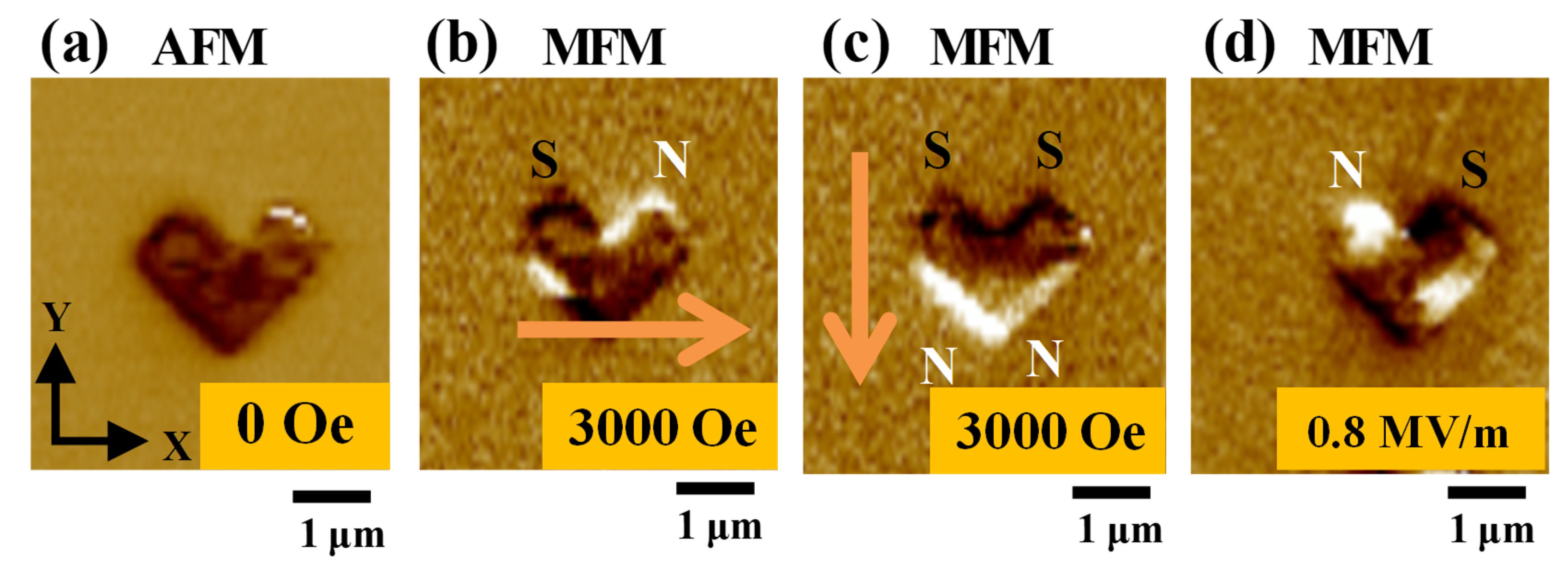
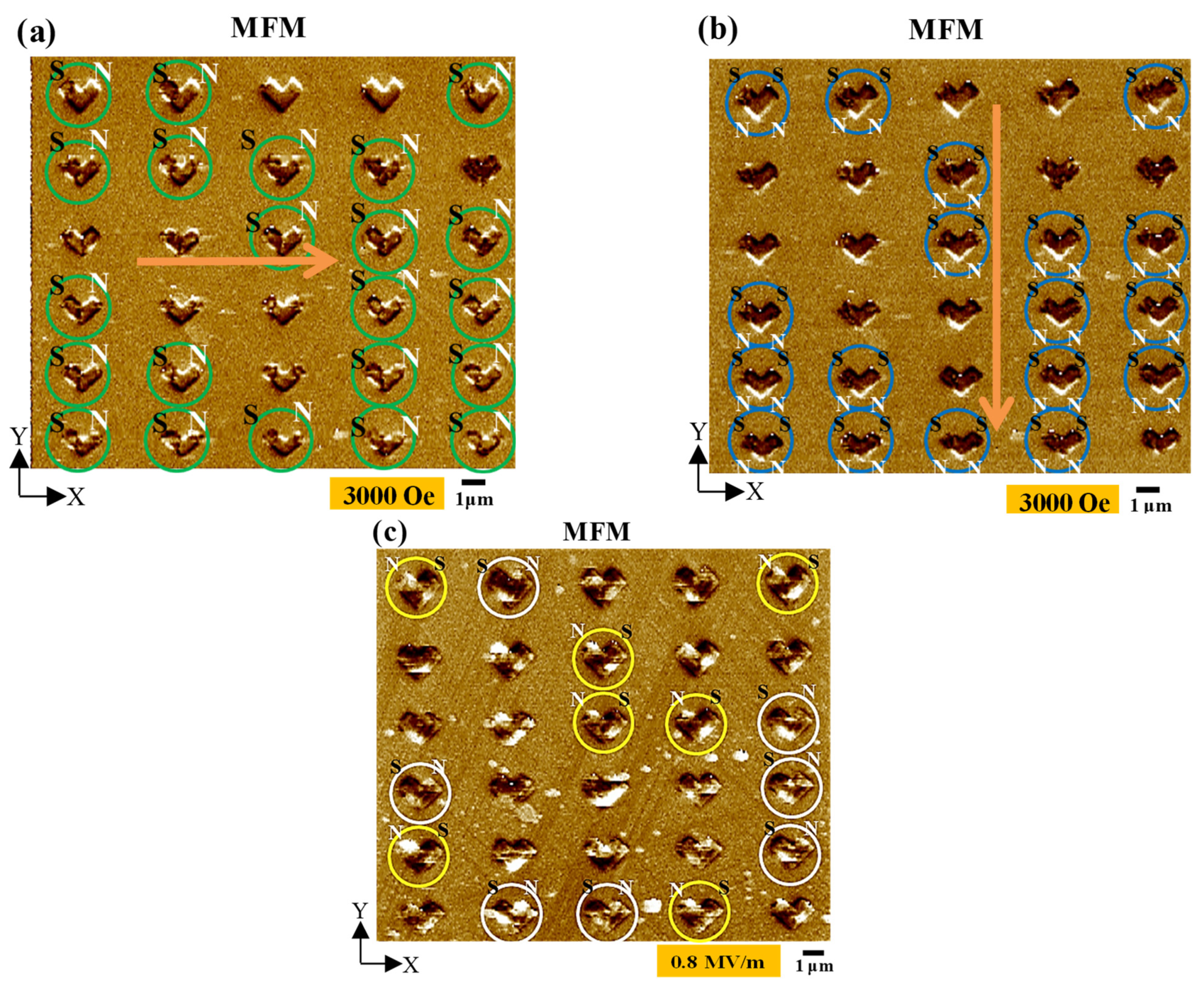
4. Results and Discussion
5. Conclusions
Author Contributions
Funding
Data Availability Statement
Conflicts of Interest
References
- Niarchos, D. Magnetic MEMS: Key issues and some applications. Sens. Actuators A Phys. 2003, 109, 166–173. [Google Scholar] [CrossRef]
- Donolato, M.; Torti, A.; Kostesha, N.; Deryabina, M.; Sogne, E.; Vavassori, P.; Hansen, M.F.; Bertacco, R. Magnetic domain wall conduits for single cell applications. Lab Chip 2011, 11, 2976–2983. [Google Scholar] [CrossRef] [PubMed]
- Yao, Z.; Wang, Y.E.; Keller, S.; Carman, G.P. Bulk acoustic wave-mediated multiferroic antennas: Architecture and performance bound. IEEE Trans. Antennas Propag. 2015, 63, 3335–3344. [Google Scholar] [CrossRef]
- Chung, T.-K.; Wong, K.; Keller, S.; Wang, K.L.; Carman, G.P. Electrical control of magnetic remanent states in a magnetoelectric layered nanostructure. J. Appl. Phys. 2009, 106, 103914. [Google Scholar] [CrossRef]
- Panduranga, M.K.; Xiao, Z.; Schneider, J.D.; Lee, T.; Klewe, C.; Chopdekar, R.; Shafer, P.; N’Diaye, A.T.; Arenholz, E.; Candler, R.N. Single magnetic domain Terfenol-D microstructures with passivating oxide layer. J. Magn. Magn. Mater. 2021, 528, 167798. [Google Scholar] [CrossRef]
- Khojah, R.; Xiao, Z.; Panduranga, M.K.; Bogumil, M.; Wang, Y.; Goiriena-Goikoetxea, M.; Chopdekar, R.V.; Bokor, J.; Carman, G.P.; Candler, R.N. Single-domain multiferroic array-addressable terfenol-D (SMArT) micromagnets for programmable single-cell capture and release. Adv. Mater. 2021, 33, 2006651. [Google Scholar] [CrossRef]
- Sohn, H.; Nowakowski, M.E.; Liang, C.-Y.; Hockel, J.L.; Wetzlar, K.; Keller, S.; McLellan, B.M.; Marcus, M.A.; Doran, A.; Young, A. Electrically driven magnetic domain wall rotation in multiferroic heterostructures to manipulate suspended on-chip magnetic particles. ACS Nano 2015, 9, 4814–4826. [Google Scholar] [CrossRef]
- Lo Conte, R.; Xiao, Z.; Chen, C.; Stan, C.V.; Gorchon, J.; El-Ghazaly, A.; Nowakowski, M.E.; Sohn, H.; Pattabi, A.; Scholl, A. Influence of nonuniform micron-scale strain distributions on the electrical reorientation of magnetic microstructures in a composite multiferroic heterostructure. Nano Lett. 2018, 18, 1952–1961. [Google Scholar] [CrossRef]
- Khojah, R.; Xiao, Z.; Panduranga, M.K.; Bogumil, M.; Wang, Y.; Goiriena-Goikoetxea, M.; Chopdekar, R.V.; Bokor, J.; Carman, G.P.; Candler, R.N. Single-cell manipulation: Single-domain multiferroic array addressable Terfenol-D (SMArT) micromagnets for programmable single-cell capture and release. Adv. Mater. 2021, 33, 2170159. [Google Scholar] [CrossRef]
- Wu, T.; Bur, A.; Wong, K.; Zhao, P.; Lynch, C.S.; Amiri, P.K.; Wang, K.L.; Carman, G.P. Electrical control of reversible and permanent magnetization reorientation for magnetoelectric memory devices. Appl. Phys. Lett. 2011, 98, 262504. [Google Scholar] [CrossRef]
- Wu, T.; Bur, A.; Kim, H.K.; Zhao, P.; Carman, G. Giant Electrical Control of Magnetic Anisotropy in Magnetoelectric Heterostructures Using (011) PMN-PT Single Crystal; SPIE: Washington, DC, USA, 2011; Volume 7978. [Google Scholar]
- Hsu, C.-J.; Hockel, J.L.; Carman, G.P. Magnetoelectric manipulation of domain wall configuration in thin film Ni/[Pb (Mn1/3Nb2/3) O3] 0.68-[PbTiO3] 0.32 (001) heterostructure. Appl. Phys. Lett. 2012, 100, 092902. [Google Scholar] [CrossRef]
- Chung, T.-K.; Wang, H.-M.; Chen, Y.-J.; Lin, S.-H.; Chu, H.-J.; Lin, P.-J.; Hung, C.-F. Magnetic-field-assisted electric-field-controlled rotation of magnetic stripe domains in a magnetoelectric Ni microbar/[Pb (Mg1/3Nb2/3) O3]0.68–[PbTiO3]0.32 heterostructure. Appl. Phys. Express 2016, 9, 043003. [Google Scholar] [CrossRef]
- Conte, R.L.; Gorchon, J.; Mougin, A.; Lambert, C.; El-Ghazaly, A.; Scholl, A.; Salahuddin, S.; Bokor, J. Electrically controlled switching of the magnetization state in multiferroic BaTiO3/CoFe submicrometer structures. Phys. Rev. Mater. 2018, 2, 091402. [Google Scholar] [CrossRef]
- Zavaliche, F.; Zhao, T.; Zheng, H.; Straub, F.; Cruz, M.; Yang, P.-L.; Hao, D.; Ramesh, R. Electrically assisted magnetic recording in multiferroic nanostructures. Nano Lett. 2007, 7, 1586–1590. [Google Scholar] [CrossRef] [PubMed]
- Chung, T.-K.; Carman, G.P.; Mohanchandra, K.P. Reversible magnetic domain-wall motion under an electric field in a magnetoelectric thin film. Appl. Phys. Lett. 2008, 92, 112509. [Google Scholar] [CrossRef]
- Wu, T.; Bur, A.; Zhao, P.; Mohanchandra, K.P.; Wong, K.; Wang, K.L.; Lynch, C.S.; Carman, G.P. Giant electric-field-induced reversible and permanent magnetization reorientation on magnetoelectric Ni/(011)[Pb (Mg1/3Nb2/3) O3](1−x)–[PbTiO3]x heterostructure. Appl. Phys. Lett. 2011, 98, 012504. [Google Scholar]
- Hockel, J.L.; Bur, A.; Wu, T.; Wetzlar, K.P.; Carman, G.P. Electric field induced magnetization rotation in patterned Ni ring/Pb (Mg1/3Nb2/3)O3](1−0.32)-[PbTiO3]0.32 heterostructures. Appl. Phys. Lett. 2012, 100, 022401. [Google Scholar] [CrossRef]
- Yao, J.; Song, X.; Gao, X.; Tian, G.; Li, P.; Fan, H.; Huang, Z.; Yang, W.; Chen, D.; Fan, Z. Electrically driven reversible magnetic rotation in nanoscale multiferroic heterostructures. ACS Nano 2018, 12, 6767–6776. [Google Scholar] [CrossRef]
- Wang, Y.; Wang, L.; Xia, J.; Lai, Z.; Tian, G.; Zhang, X.; Hou, Z.; Gao, X.; Mi, W.; Feng, C. Electric-field-driven non-volatile multi-state switching of individual skyrmions in a multiferroic heterostructure. Nat. Commun. 2020, 11, 3577. [Google Scholar] [CrossRef]
- Li, X.; Singh, H.; Bao, Y.; Luo, Q.; Li, S.; Chatterjee, J.; Goiriena-Goikoetxea, M.; Xiao, Z.; Tamura, N.; Candler, R.N. Energy Efficient All-Electric-Field-Controlled Multiferroic Magnetic Domain-Wall Logic. Nano Lett. 2023, 23, 6845–6851. [Google Scholar] [CrossRef]
- Chung, T.-K.; Keller, S.; Carman, G.P. Electric-field-induced reversible magnetic single-domain evolution in a magnetoelectric thin film. Appl. Phys. Lett. 2009, 94, 132501. [Google Scholar] [CrossRef]
- Zavaliche, F.; Zheng, H.; Mohaddes-Ardabili, L.; Yang, S.; Zhan, Q.; Shafer, P.; Reilly, E.; Chopdekar, R.; Jia, Y.; Wright, P. Electric field-induced magnetization switching in epitaxial columnar nanostructures. Nano Lett. 2005, 5, 1793–1796. [Google Scholar] [CrossRef] [PubMed]
- Taniyama, T.; Akasaka, K.; Fu, D.; Itoh, M.; Takashima, H.; Prijamboedi, B. Electrical voltage manipulation of ferromagnetic microdomain structures in a ferromagnetic/ferroelectric hybrid structure. J. Appl. Phys. 2007, 101, 09F512. [Google Scholar] [CrossRef]
- Wu, T.; Bur, A.; Hockel, J.L.; Wong, K.; Chung, T.-K.; Carman, G.P. Electrical and mechanical manipulation of ferromagnetic properties in polycrystalline nickel thin film. IEEE Magn. Lett. 2011, 2, 6000104. [Google Scholar]
- Zhang, J.; Xue, W.; Su, T.; Ji, H.; Zhou, G.; Jiang, F.; Quan, Z.; Xu, X. Nanoscale magnetization reversal by magnetoelectric coupling effect in Ga0.6Fe1.4O3 multiferroic thin films. ACS Appl. Mater. Interfaces 2021, 13, 18194–18201. [Google Scholar] [CrossRef] [PubMed]
- Wu, T.; Bur, A.; Wong, K.; Leon Hockel, J.; Hsu, C.-J.; Kim, H.K.; Wang, K.L.; Carman, G.P. Electric-poling-induced magnetic anisotropy and electric-field-induced magnetization reorientation in magnetoelectric Ni/(011)[Pb(Mg1/3Nb2/3)O3](1-x)-[PbTiO3]x heterostructure. J. Appl. Phys. 2011, 109, 07D732. [Google Scholar] [CrossRef]
- Ryu, J.; Carazo, A.V.; Uchino, K.; Kim, H.-E. Magnetoelectric properties in piezoelectric and magnetostrictive laminate composites. Jpn. J. Appl. Phys. 2001, 40, 4948. [Google Scholar] [CrossRef]
- Taniyama, T.; Nakatani, I.; Namikawa, T.; Yamazaki, Y. Resistivity due to domain walls in Co zigzag wires. Phys. Rev. Lett. 1999, 82, 2780. [Google Scholar] [CrossRef]
- Wieser, R.; Nowak, U.; Usadel, K.-D. Domain wall mobility in nanowires: Transverse versus vortex walls. Phys. Rev. B 2004, 69, 064401. [Google Scholar] [CrossRef]
- Parkin, S.S.; Hayashi, M.; Thomas, L. Magnetic domain-wall racetrack memory. Science 2008, 320, 190–194. [Google Scholar] [CrossRef]
- Goolaup, S.; Ramu, M.; Murapaka, C.; Lew, W. Transverse domain wall profile for spin logic applications. Sci. Rep. 2015, 5, 9603. [Google Scholar] [CrossRef] [PubMed]
- Cheng, C.C.; Lin, S.H.; Chen, Y.J.; Wang, H.M.; Chu, H.J.; Hung, C.F.; Lin, P.J.; Chung, T.K. A novel nanoelectromagnetic system using multiferroic/magneto electric Ni nano-chevron/PMN-PT heterostructure to demonstrate an electric field controlled permanent magnetic single domain transformation. In Proceedings of the 2018 ASME Information Storage & Processing Systems (ISPS2018), San Francisco, CA, USA, 29–30 August 2018. ISPS2018-8502. [Google Scholar]
- Liang, C.Y.; Keller, S.M.; Sepulveda, A.E.; Bur, A.; Sun, W.Y.; Wetzlar, K.; Carman, G.P. Modeling of magnetoelastic nanostructures with a fully coupled mechanical-micromagnetic model. Nanotechnology 2014, 25, 435701. [Google Scholar] [CrossRef] [PubMed]
- Liang, C.Y.; Keller, S.M.; Sepulveda, A.E.; Sun, W.Y.; Cui, J.; Lynch, C.S.; Carman, G.P. Electrical control of a single magnetoelastic domain structure on a clamped piezoelectric thin film-analysis. J. Appl. Phys. 2014, 116, 123909. [Google Scholar] [CrossRef]
- Kundu, A.A.; Chavez, A.C.; Keller, S.M.; Carman, G.P.; Lynch, C.S. 360° deterministic magnetization rotation in a three-ellipse magnetoelectric heterostructure. J. Appl. Phys. 2018, 123, 104105. [Google Scholar] [CrossRef]
- Keller, S.M.; Liang, C.Y.; Sepulveda, A.E.; Carman, G.P. Voltage control of single magnetic domain nanoscale multiferroic heterostructure. In Proceedings of the 2015 Transducers—2015 18th International Conference on Solid-State Sensors, Actuators and Microsystems (TRANSDUCERS), Anchorage, AK, USA, 21–25 June 2015; pp. 796–798. [Google Scholar]
- Gilbert, I.; Chavez, A.C.; Pierce, D.T.; Unguris, J.; Sun, W.Y.; Liang, C.Y.; Carman, G.P. Magnetic microscopy and simulation of strain-mediated control of magnetization in PMN-PT/Ni nanostructures. Appl. Phys. Lett. 2016, 109, 162404. [Google Scholar] [CrossRef]


Disclaimer/Publisher’s Note: The statements, opinions and data contained in all publications are solely those of the individual author(s) and contributor(s) and not of MDPI and/or the editor(s). MDPI and/or the editor(s) disclaim responsibility for any injury to people or property resulting from any ideas, methods, instructions or products referred to in the content. |
© 2023 by the authors. Licensee MDPI, Basel, Switzerland. This article is an open access article distributed under the terms and conditions of the Creative Commons Attribution (CC BY) license (https://creativecommons.org/licenses/by/4.0/).
Share and Cite
Cheng, C.-C.; Chen, Y.-J.; Lin, S.-H.; Wang, H.-M.; Lin, G.-P.; Chung, T.-K. Magnetic-Field-Assisted Electric-Field-Induced Domain Switching of a Magnetic Single Domain in a Multiferroic/Magnetoelectric Ni Nanochevron/[Pb(Mg1/3Nb2/3)O3]0.68–[PbTiO3]0.32 (PMN–PT) Layered Structure. Micromachines 2024, 15, 36. https://doi.org/10.3390/mi15010036
Cheng C-C, Chen Y-J, Lin S-H, Wang H-M, Lin G-P, Chung T-K. Magnetic-Field-Assisted Electric-Field-Induced Domain Switching of a Magnetic Single Domain in a Multiferroic/Magnetoelectric Ni Nanochevron/[Pb(Mg1/3Nb2/3)O3]0.68–[PbTiO3]0.32 (PMN–PT) Layered Structure. Micromachines. 2024; 15(1):36. https://doi.org/10.3390/mi15010036
Chicago/Turabian StyleCheng, Chih-Cheng, Yu-Jen Chen, Shin-Hung Lin, Hsin-Min Wang, Guang-Ping Lin, and Tien-Kan Chung. 2024. "Magnetic-Field-Assisted Electric-Field-Induced Domain Switching of a Magnetic Single Domain in a Multiferroic/Magnetoelectric Ni Nanochevron/[Pb(Mg1/3Nb2/3)O3]0.68–[PbTiO3]0.32 (PMN–PT) Layered Structure" Micromachines 15, no. 1: 36. https://doi.org/10.3390/mi15010036
APA StyleCheng, C.-C., Chen, Y.-J., Lin, S.-H., Wang, H.-M., Lin, G.-P., & Chung, T.-K. (2024). Magnetic-Field-Assisted Electric-Field-Induced Domain Switching of a Magnetic Single Domain in a Multiferroic/Magnetoelectric Ni Nanochevron/[Pb(Mg1/3Nb2/3)O3]0.68–[PbTiO3]0.32 (PMN–PT) Layered Structure. Micromachines, 15(1), 36. https://doi.org/10.3390/mi15010036